Microscopic Model for Intersubband Gain from Electrically Pumped Quantum-Dot Structures
Abstract
We study theoretically the performance of electrically pumped self-organized quantum dots as a gain material in the mid-IR range at room temperature. We analyze an AlGaAs/InGaAs based structure composed of dots-in-a-well sandwiched between two quantum wells. We numerically analyze a comprehensive model by combining a many-particle approach for electronic dynamics with a realistic modeling of the electronic states in the whole structure. We investigate the gain both for quasi-equilibrium conditions and current injection. Comparing different structures we find that steady-state gain can only be realized by an efficient extraction process, which prevents an accumulation of electrons in continuum states, that make the available scattering pathways through the quantum dot active region too fast to sustain inversion. The tradeoff between different extraction/injection pathways is discussed. Comparing the modal gain to a standard quantum-well structure as used in quantum cascade lasers, our calculations predict reduced threshold current densities of the quantum dot structure for comparable modal gain. Such a comparable modal gain can, however, only be achieved for an inhomogeneous broadening of a quantum-dot ensemble that is close to the lower limit achievable today using self-organized growth.
I Introduction
Much research on light emitters in the mid-infrared range has been focused on quantum cascade lasers (QCL), QCL1 ; QCL2 ; QCL3 ; QCL4 ; QCL5 ; Harrison1 ; Harrison2 ; Harrison6 ; Ines1 ; Ines2 which are complex structures consisting of hundreds of coupled quantum wells (QWs). QCLs can produce a high output power and operate up to and above room temperature. MIR4 ; MIR3 ; MIR2 ; MIR5 ; QCL6 ; QCL7 QWs usually emit light only in-plane due to the transverse magnetic (TM) polarization of the intersubband transition. To achieve emission perpendicular to the surface from intersubband transitions one needs to fabricate wavelength specific surface output couplers. MIR6 Mid-infrared lasers emit in a frequency range close to thermal energies, so that there may be considerable thermal energy losses. The development of more efficient emitters is therefore an important problem. QCL3 ; Harrison6 The use of nanostructures with a three dimensional confinement leads to discrete level energies and thus limits the phase space for the interaction with phonons, which makes nonradiative recombinations much less likely. bottleneck1 ; bottleneck2 ; MIR13 For instance, a magnetic field leads to an increased efficiency of QCLs due to the occurrence of quantized electronic Landau levels. MIR8 ; Harrison8 Also a quantum-dash cascade structure was proposed. quantum-dash
Another possibility is to use self-assembled quantum dots (QDs).QDcascade Experimental results have demonstrated nonradiative relaxation times that are orders of magnitude longer than in QW structures. intro11 ; MIR12 ; intro13 There have been studies of midinfrared photodetectors using QDs, MIR15 ; MIR16 and optimization issues have been addressed. MIR2:3 In addition the room temperature ultraweak absorption of a single buried semiconductor QD was measured. MIR2:5 Also type-II InAsSb/InAs QDs for midinfrared applications have been investigated MIR2:1 and midinfrared photoluminescence of epitaxial PbTe/CdTe QDs has been studied. MIR2:4
QD intersubband transitions are particularly promising for mid-infrared wavelengths. intraband-DWELL-PDetector These transitions allow light emission normal to the growth direction. Additionally, they are a basic requirement for the realization of a QCL consisting of QDs. Steps in this direction include the demonstration of midinfrared electroluminescence at low temperatures, MIR2:6 ; MIR19 ; MIR20 and a theoretical proposal of TE-polarized optical gain through a ruby-type three level scheme. rubyscheme While QD midinfrared emission of devices using additional interband transitions has also been proposed, MIR18 such a scheme would be only feasible for weak cavity fields.
Recently, progress in room temperature midinfrared electroluminescence from QDs was made. midinfrared1 ; el_roomtemp An essential part of the proposed structure in Ref. midinfrared1, is electron tunneling between QW and QD states. The properties of related tunneling processes between localized and continuum states in self-organized QD structures have been separately investigated. tunneling_th ; tunneling_exp
The present paper presents a theoretical model for a structure similar to Ref. midinfrared1, . We assume a heterostructure consisting of a thin active layer of QDs embedded in a QW (a so-called DWELL structure), which is, in turn sandwiched between two QWs. We refer to this as a QW-QD-QW heterostructure. Because QW-QD-QW heterostructures include a dots-in-a-well (DWELL) structure, not only electron tunneling between QW and QD states but also typical effects of density-dependent carrier dynamics for DWELL heterostructures are of importance. prasankumar Using electronic eigenstates for the whole structure as input, we solve the dynamical equations for the electronic level occupations and for the important coherences in the system under investigation. In doing so we distinguish between intra-QD, intra-QW and QD-QW electron scattering and calculate the underlying electron-phonon and electron-electron scattering processes microscopically following a many-particle approach that includes, in particular, the effects of the electron-phonon interactions on the QD states PQE_Review . Using different models for the excitation process, we determine the achievable inversion (gain) in the active medium. Based on the numerical results, we discuss possible optimizations of the design of AlGaAs/InGaAs QW-QD-QW structures as active material for midinfrared lasers. To the best of our knowledge, a microscopic theoretical investigation and optimization for the capability of those devices for midinfrared laser applications is still missing.
In the present paper we focus on some physical properties and parameter dependencies associated with the gain achievable in QDs by current injection. This does not solve all the numerous technical challenges of a QD laser device but may contribute some design criteria for future devices. Furthermore, we present a comparison between QD-QCL and QW-QCL devices. We focus on the active material and do not include collector regions as in QD-QCLs. However, the results of the analysis done are transferable to periodic structures (such as a QD-QCL), if small carrier losses in the collector region are neglected.
This paper is organized as follows. In Sec. II we describe two QW-QD-QW structures that represent possible designs for a gain material in the infrared, and calculate the electronic band lineup and wave functions. There is a brief review of the semiconductor Bloch equations and their scattering contributions that we use to describe the structures under consideration in Sec. III. In Sec. IV.1 we investigate the conditions for which inversion between the ground and degenerate excited states in the QDs can be achieved, assuming fixed carrier densities in the QWs. The small signal gain is determined from the population inversion. In Sec. IV.2 we incorporate carrier injection (extraction) into the model and compare the different structures. In Sec. IV.3, we present numerical results for stronger fields and identify a range of parameters for which gain in the midinfrared at room temperature is feasible. Additionally, the tradeoff between the different injection (extraction) pathways and the consequences of leakage are discussed in Sec. IV.4. Finally, in Sec. V, we compare a standard QW-QCL design from Ref. Harrison1, to our QD-QCL alternative to illustrate the possible potential of QD-QCLs.
II Electronic structure of a QW-QD-QW system
.
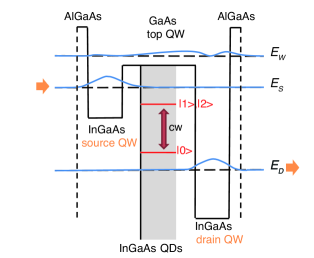
We describe here a QW-QD-QW system with a QD layer (DWELL structure) designed to emit in the midinfrared and potentially suitable as intersubband-laser gain medium. Fig. 1 shows a structure designed to rely on electron-phonon scattering for creating inversion in the QDs.
For the structure “A” in Fig. 1 we assume a cw field resonant with the transition between the lowest electronic level of the QD and the excited level , , which are degenerate. If a quasi-equilibrium Fermi-Dirac distribution is maintained in the DWELL structure, a population inversion for the optically active states in the QD is not possible in steady-state, so that it is necessary to extract carriers out of the lowest electronic level of the DWELL structure. This is achieved by an additional “drain” QW with electronic band edge that is offset roughly by a LO phonon energy from the lowest electronic level in the QD, i.e., , where is smaller than a few meV. We keep in the calculation because a perfect lineup of the structure is not necessary. Since the wave-functions of the QD and drain QW states do not overlap appreciably, the scattering process is slow compared to a similar scattering process between the extended states and localized states in the DWELL structure. We refer to the extended states in the DWELL structure as “top” QW even though they are not pure plane waves, but have been orthogonalized to the localized QD levels. In particular, electron-electron scattering between QD and top QW states for a significant occupation of the top QW is extremely efficient. If the source for carriers is the top QW, the relaxation from the QD state to the states of the drain QW will be not efficient enough to extract electrons from level , and thus keep the transition inverted. Carrier injection is therefore done in our structure from a second QW, referred to as “source” QW with a electronic band edge offset by an LO phonon energy from the excited levels and , i.e., , where is also smaller than a few meV. We further assume in the following an energy difference , which leads to a so-called phonon bottleneck effect because transitions between the discrete electron states are inhibited. bottleneck1 ; MIR13 To facilitate steady-state population inversion for the optical active states electron-electron scattering processes that are assisted by transitions in the top QW should be suppressed as much as possible. This is achieved by the energy difference between the excited QD levels and the band edge of the top QW. With such a band lineup the carrier-density of the top QW and the electron-electron scattering contribution from this density is kept as small as possible.
With the band lineup described so far, it remains to optimize the injection and removal of carriers for the operation as a light emitter. To this end, the source and the drain QW wave functions need to have significant overlap with the QD wave functions, but the layers cannot be too close to each other to avoid electrical breakdown between the source- and drain-QW.
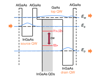
As a variation of the structure “design” we will also consider carrier removal from the extended states in the top QW in addition to the removal process through the QD states. Removal of carriers is provided through subbands of the surrounding heterostructure. In the structures analyzed here, the composition and shape of the electronic structure leads to a top QW with an admixture of the first excited subband of the drain QW, which realizes an efficient overlap of the drain QW and top QW with the surrounding heterostructure. A small width of the source- and drain-QW helps to increase the overlap further. However, in our investigation we do not include the design of the surrounding heterostructure, which is indicated by the broken lines at the left and right side of the band lineups in Figs. 1 and 2.
We now present in some details the geometry and material parameters used for the calculation of the electronic structures shown in Fig. 1, which incorporates the design principles discussed so far. We assume an ensemble of In0.75Ga0.25As QDs on a wetting layer with a thickness of nm embedded in the GaAs top QW. The geometry of the QDs is a truncated pyramid with facets. The QDs have a base of nm and height of nm. For an overlap-optimized structure (see Fig. 1) the GaAs top QW has a width of nm and the bottom of the wetting layer has a distance of nm to the source QW. The In0.12Ga0.88As source QW and the In0.38Ga0.62As drain QW have both a width of nm. The whole system is embedded in an Al0.1Ga0.9As barrier.
The electronic structure is calculated by theory homepage as described in Appendix A. For computational reasons, we treat the calculation of the three-dimensional QD states separately from the calculation of the one-dimensional envelope of the QWs, and orthogonalize the three-dimensional QW states to describe the whole system. For the QD we obtain a ground and two degenerate excited states. For the source-, the top- and the drain-QW only one confined subband exists, respectively. The excited drain-QW subband is mixed with the top QW confined subband as discussed above. For the combined system the line up of states are compiled in Table 1. The transition energy between the optical active states of the QD is meV. This corresponds to a mid-infrared wavelength of m.
| Band edge of … | Symbol | Energy (meV) |
|---|---|---|
| top QW | ||
| source QW | ||
| drain QW | ||
| QD state | Symbol | Energy (meV) |
| , | ||
For comparison, structure “B”, shown in Fig. 2 is introduced, which is less aggressively optimized for wave-function overlap and incorporates some safeguards against electrical breakdown and current leakage. To this end the distance between source- and drain-QW is increased, and an Al0.1Ga0.9As barrier between the source QW and the top QW is introduced. In addition, the barrier between source QW and top QW allows both QWs to be addressed separately by an injection and extraction processes. In particular, in structure B carriers can be extracted from the drain QW and the top QW, as indicated in Figs. 2 and 3. The barrier has a width of nm and the total distance between source and drain QW is 14 nm. The wetting layer is 5 nm above the source QW. To obtain comparable energies, we corrected the composition of the source QW to In0.13Ga0.87As for the numerical calculation. All other parameters remain unchanged, including the carrier injection process. Note, however, that for structure A we assume carrier extraction from the drain QW only. In the following, we thus compare the performance of structures with optimized wave-function overlap (structure A) and optimized carrier extraction (structure B).
III Semiconductor Bloch equations
The dynamics of the polarizations and carrier distributions at the single-particle level are calculated in the framework of the semiconductor Bloch equations for the reduced single-particle density matrix. We denote in the following electron levels in the QD with . For the optical active states of interest one obtains the following equations of motion for the “intra(electron-)band” polarizations
| (1) |
where is a decay rate for the polarization. For the time evolution of the electron populations one obtains
| (2) |
The coherent contributions of the above equations containing the transition frequencies and Rabi frequencies where is the electric field at the position of the QD.
The term describes the scattering contributions in the dynamical equations for the electron distributions and contains the influence of electron-electron Coulomb and electron-phonon scattering. Their theoretical treatment is contained in the following section.
In the semiconductor Bloch equations (1) and (2) also Hartree-Fock energy renormalizations arise, which can reach a few meV for highly populated QD states. However, energy shifts of only a few meV do not affect the scattering behavior significantly. Moreover, the Hartree-Fock energy renormalization has the same effect on the steady-state result of the population inversion as a slight change of the material composition. An optimization of the electronic structure including Hartree-Fock energy renormalizations would require inverse quantum-engineering as described in Ref. Ines1, , which is beyond the scope of the present paper. We therefore neglect renormalization due to Coulomb interaction. For the calculation with an optical field in Sec. IV.3, we are mainly interested in the qualitative dependence on the optical field intensity, which is treated as a parameter in our calculation. Thus we also neglect Hartree-Fock contributions that result in and of the Rabi energy, which would have to be included in a more comprehensive calculation where the dynamics of the optical field is also included.
III.1 Scattering contributions
The scattering contribution includes both electron-electron and electron-phonon scattering. Our treatment is described in more detail in Appendix B, where the explicit expressions are given. Here we only summarize our approach.
While electrons interact with longitudinal acoustic (LA) and longitudinal optical (LO) phonons, scattering effects due to acoustic phonons in QDs are estimated to be very inefficient,SQD as long as level spacing of the QDs is much larger as the typical energy range of the acoustic phonons coupled to the QDs, i.e., below a few meV in InGaAs QDs or QD molecules.Giannozi ; Zimmermann1
Scattering processes involving QD states connect discrete levels so that the influence of level broadening is much more pronounced than for scattering between continuum states in QWs. Thus, we follow Ref. QDM, and introduce an effective quasi-particle broadening for the scattering contributions. By using an effective quasi-particle broadening we work with polarons, i.e., quasi-particles that include the effect of the coupling to phonons, instead of the “naked” QD electronic levels. We have determined this broadening from single-pole approximations to the zero-density QD polaronic spectral functions, see also in Ref. QDM, , in the style of Ref. Jahnke4, ; Jahnke2, and neglected the Coulomb-interaction contribution to the effective quasi-particle broadening. This is a valid approximation, if the continuum states, i.e., especially the top QW, are not appreciably populated by carriers, which is necessary if gain, i.e., inversion, for the optically active transition is desired, see Sec. IV.1.
A constant level broadening around , i.e., , was calculated for typical InAs QDs. dissertation Here, we assume the level broadening of a typical InAs QD, because a precise calculation of the level broadening of the QD in our QW-QD-QW structure is too demanding with respect to computing time. The QD under investigation has rather a large level spacing. That is why the stated value for the broadening tends to result to an overestimation. Because a small broadening reduces the electron-phonon relaxation from the excited to the ground state of the QD, the gain is reduced by an overestimation of the broadening. Thus, to be on the safe side its better to slightly overestimate rather than to underestimate the broadening of the QD states. All in all, the precise value of does not affect the statements of our theoretical analysis, but it is important to get its order of magnitude right.
With the considerations above it turns out that the relaxation or scattering for the carrier distributions cannot easily be computed using Fermi’s Golden Rule arguments because there is no straightforward energy conservation for transitions between polarons. Thus, the calculated constant level broadening referring to the effect of the electron-phonon interaction on the polaronic spectrum in the form of complex renormalized energies of a single-particle QD state has to be incorporated into the explicit scattering expressions by
| (3) |
where is a negligible energy shift (HF correction and a small correlation contribution). The broadening of the level is entirely due to correlations. This incorporation is done by following Ref. QDM, for the derivation of the electron-phonon and electron-electron scattering. In contrast to Ref. QDM, all coherences are neglected. This is especially in the case of a small signal gain a valid approximation. We also assume that only conduction band states are involved in the scattering process, because only electrons in the conduction band are injected and extracted from the system under investigation. The explicit formula expressions for the electron-phonon and electron-electron scattering is given in Appendix B.
III.2 Model for carrier injection (extraction)
We next include a simplified model for current injection in the structure described above. We assume that the current injects carriers into the left side of the structure, i.e., the source QW, and removes them from the right side, i.e., drain or top QW. For an effective injection (extraction) of carriers from a QW, energetically close and local nearby subbands have to be provided from the surrounding heterostructure.
For the inclusion of the process, we extend the Bloch equations for the source QW, according to Ref. chowbook1, , by a carrier injection term of the form
| (4) |
where the Pauli blocking factor prevents the pump from injecting carriers in occupied states. Further, denotes an injection rate and is a Fermi-Dirac pump distribution.
The pump distribution model in the form (4) attempts to capture in a simple form the details of the injection process. It is based on the assumption that by the time the injected carriers reach the source QW they have thermalized by collisions and therefore their dependence can be described by a quasi-equilibrium pump distribution with the characteristic carrier density and the characteristic temperature as parameters, which are kept constant. This distribution is weighted by an injection rate . The temperature entering is taken to be the lattice temperature. The pump distribution should not be confused with a Fermi-Dirac distribution in the QW. Note that we use the injection rate as the independent parameter and calculate the steady-state current density via where is the normalization area of the quantum well. This expression for the current will be used to compare to similar calculations for quantum well structures in Section V below.
To model the extraction of carriers by transport of carriers from the drain or top QW to the right side of the structure, we extend the Bloch equations for the QWs by the simple rate equation
| (5) |
where is the occupation of the QW state .
With regard to the injection model we should also briefly discuss changes introduced to the band lineup in a biased structure. For realistic fields of several 10 kV/cm along the growth axis one expects an energy shift of a few meV between nearby QW and QD states. In agreement with Ref. Lim, we neglect these small energy corrections for the thin QW-QD-QW heterostructure under investigation. For a potential drop of more than about 15 meV over the active region, the energy difference between the source QW band bottom and the excited QD level becomes too large for efficient carrier injection. In this case the design of the “cold” structure needs to be changed such that the bias-induced shift leads to a level lineup close to the one described in Figs. 1 and 2. In particular, for a field of 36 kV/cm as chosen in Sec. V the “cold” structure needs to be changed to a source-QW composition of In0.19Ga0.81As and a drain-QW composition of In0.33Ga0.67As to obtain approximately the same level lineup as described above.
IV Numerical results
IV.1 Inversion (gain) for fixed QW carrier-densities
In this section we investigate under which conditions regarding the carrier densities of the QWs an inversion between the ground and degenerate excited states in the QDs is possible. Therefore we investigate the behavior of the population inversion in the QDs for fixed quasi-equilibrium distributions in the QWs. Because the carrier densities in the QWs are kept fixed, no injection (removal) processes are included.
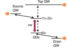
In the numerical calculation we start with given QW carrier densities and an initially empty QD system. Importantly, electron-phonon and electron-electron scattering described by Eqs. (18) and (LABEL:electron-electron) leads to QD-QW electron scattering as well as intra-QD scattering processes (see scattering processes (iii) and (iv) depicted in Fig. 3). The carrier distributions are evolved until a steady-state is reached.
For a weak optical field in resonance with the transition between the lowest and excited states of the QD the steady-state distributions remain unchanged. The intensity gain for such a weak optical fields is given by
| (6) |
where meV is the transition energy, (GaAs) the background refractive index of the host material, cm-2 the QD density, nm the heights of the active region, nm the dipole moment, meV the polarization dephasing and the inversion of the optically active states. The intersubband dipole moment nm is five times larger than the interband dipole moment for the transition between the electron and hole ground state, which already has an appreciable magnitude. Thus, for the same inversion , the gain on the intersubband transition is larger than that on an interband transition in the QD. The choice of the polarization dephasing of meV is motivated by the restrictions that it has to be higher than intersubband dephasing for the case of unpopulated QD scattering states and a small carrier density in the QWs ( meV),QDM but lower than an interband dephasing with an appreciable population in the QD scattering states ( up to meV). highdeph We will plot the small signal gain in addition to the inversion between the optically active states in the following.
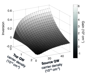
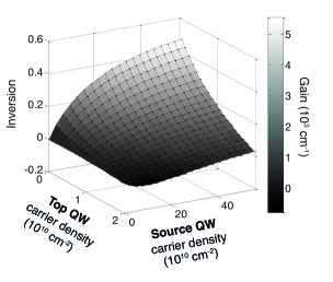
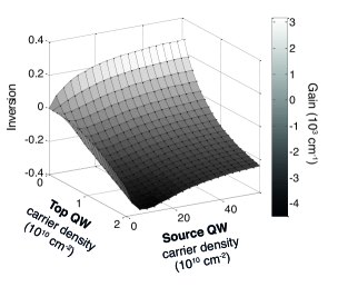
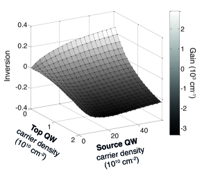
Figure 4 and Fig. 5 shows the population inversion and gain for the QD transition in structure A as a function of carrier densities in the top and source QWs. The drain QW is assumed to be empty, which is a “best case” assumption for carrier extraction from the active region. In Fig. 4 the lattice temperature is 150 K. For an empty top QW and a negligible carrier density in the source QW the gain is obviously zero. Up to a source-QW density of cm-2 the gain rises steeply, levels off in the range between cm-2 to cm-2, and reaches saturation over cm-2. An increasing carrier density in the top QW for a fixed carrier density in the source QW leads to a rapid decrease in the gain. For a carrier density of approximately cm-2 no gain remains, and for higher densities in the top QW only absorption exists.
Figure 5 depicts the results of a calculation analogous to Fig. 4, but for a lattice temperature of 300 K. The qualitative analysis remains the same, but the gradient of the gain is lower for increasing source-QW and top-QW carrier densities. In particular, the gain reaches saturation for higher carrier densities of the source QW.
We now repeat these calculations for structure B. Fig. 6 and Fig. 7 show the results for lattice temperatures of 150 K and 300 K, respectively. The overall dependence of the gain on the source-QW and top-QW densities for structure B is similar to that of structure A. However, the saturated gain is clearly smaller and the dependence of the gain on the densities in the source QW and top QW is more pronounced. In particular, absorption occurs already for top-QW carrier densities below cm-2, whereas for structure A there is still gain in this top-QW density range.
IV.2 Inversion (gain) with carrier injection
The above numerical results show that a carrier population in the top QW, i.e., the QD scattering states, has a detrimental effect on the gain. Further, it is shown in the present section that an accumulation of carriers in the top QW precludes a steady-state inversion (gain) in structures A and B, if one includes a model for carrier injection. To reach a steady-state gain one therefore has to counteract the piling up of population in the top QW. We propose to achieve this by removing carriers from these states directly as described in Sec. II, and analyze the dynamics with the additional carrier extraction in some detail. We will do these calculations for structure B because in that structure source and top QW states are separated by a barrier so that source and top QW can be better addressed separately by an injection/extraction process. For comparison we will also analyze the behavior of structure A with carrier injection, but we will always assume only extraction from the drain QW for structure A.
The basic dynamical equations are Eqs. (18) and (LABEL:electron-electron) for electron-phonon and electron-electron scattering, but now including carrier injection terms (4) and (5). In particular, the processes (i), (iii) and (iv) depicted in Fig. 3 are now considered. The pump distribution of the injection (extraction) process depends on the particular device in which the QW-QD-QW structure is embedded. Unless otherwise specified, we assume and lattice temperatures of K and K, respectively. Note that in addition to intra-QD electron scattering processes and QD-QW electron scattering processes, also intra-QW electron scattering processes occur. All the following numerical results are again computed starting from an initially empty QW and QD system and evolve the carrier distribution until a steady-state is reached.
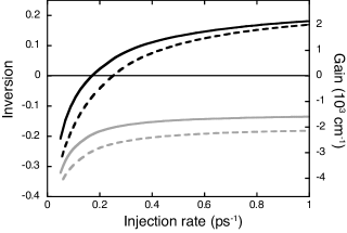
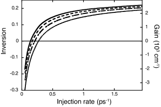
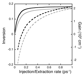
We first investigate whether a steady-state inversion, i.e., gain, can be achieved for structure A or B. Figure 8 plots the population inversion and gain for the QD transition versus the injection rate for structure A and B. For structure A the inversion rises with increasing injection rates but saturates at negative values for a lattice temperatures of K and for K. The inversion for a lattice temperature of K exceeds that for K at all injection rates. This can be expected from the increased efficiency of electron-phonon relaxation between the QD states at higher temperatures, which works against an inversion on the QD intersubband transition. However, the difference becomes smaller with increasing injection rate. For structure B the inversion also rises with increasing injection rate and reach a saturation value, which is positive: For injection rates above 1.2 ps-1 a saturation value of the inversion around is reached.
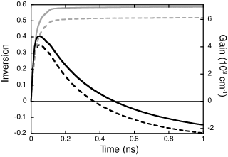
For a more detailed analysis of these results, in Fig. 9 and Fig. 10 we look at the time dependence of the population inversion for a fixed injection rate of for structure A and B, respectively. A calculation including both electron-phonon and electron-electron scattering (“ep+ee”) is compared to a calculation including only electron-phonon scattering (“ep”). Both calculations are done for lattice temperatures of 150 K and 300 K.
Fig. 9 plots the population inversion for the QD transition versus time for structure A. As long as the top-QW states are essentially empty, the ep+ee and the ep results are very similar. After a few tens of picoseconds the top-QW states are significantly populated, and electron-electron scattering becomes more efficient for the dynamics. As already discussed in Sec. IV.1 top-QW assisted QD electron relaxation becomes more important. Further, source-QW assisted QD electron capture and source-QW assisted QD electron relaxation contribute to different results for the inversion. In addition, the electron-electron scattering leads to a faster and more homogeneous redistribution of carriers in the QWs. Taken together, very different electronic distributions (with different electron densities) are reached after a few ns. The net effect is that the achievable inversion is negative for the ep+ee and positive for the ep calculation in steady-state.
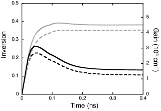
Figure 10 shows the same plot for structure B. The ep calculation for structure B is similar to that of structure A shown in Fig. 9, with structure A leading to higher gain (inversion). The important difference is between the “full”, namely, ep+ee, calculations. Here, the initial dynamics over a few tens of ps is similar to that of structure A, but much different when the carrier density rises and the influence of electron-electron scattering becomes pronounced. Since the extraction from drain and top QW states limits the carrier density in the drain and top QW, the inversion remains positive for all times and leads to a positive gain in steady state. As already mentioned in Sec. IV.1 above, structure A performs better for fixed carrier densities in the source QW. But if a carrier injection model is included, only in structure B (with carrier extraction from the top-QW states) steady-state gain can be realized. We will therefore focus on structure B in the following.
We also investigate how the carrier density of the pump distribution affects the results. As already mentioned, we treat the pump distribution as a parameter. Fig. 11 shows the population inversion and gain for the QD transitions versus injection rate for structure B for different carrier densities and a lattice temperature of 150 K. More precisely, we choose , , and for a comparison. For larger , lower injection rates are necessary to achieve similar gain values. However, apart from that, the has no decisive influence on the gain “dynamics”. Thus the variation of injection rate allows one to determine the important characteristics of the QW-QD-QW active region.
IV.3 Strong-signal effects
In this section we go beyond small-signal gain results by including an externally controlled optical field. The optical field may be the field in an optical amplifier or in a laser cavity. We run a dynamical calculation for the densities and the optical polarizations based on the semiconductor Bloch equations, i.e., (1) and (2). Again electron-phonon and electron-electron scattering is included for the whole system under investigation, in particular, the processes (i)-(iv) depicted in Fig. 3 contribute. We are interested in the dependence of the steady-state inversion , or equivalently the gain , see Eq. (6), on the optical field intensity, and we analyze exclusively structure B.
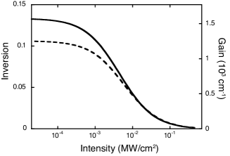
The inversion and gain achievable with structure B versus field intensity for a lattice temperature of K and K are depicted in Fig. 12. We assumed a fixed injection rate of with for the pump distribution. The weak field result is recovered for small field intensities below , as it should be. For increasing field intensity the inversion and the gain decrease, because the optical field leads to a stimulated recombination of carriers and reduces the inversion. For field intensities between and the inversion, i.e. gain, is still positive, but decreases rapidly. For field intensities above no significant inversion or gain is observed. While for weak field intensities the lower lattice temperatures has the higher gain, this difference is strongly reduced with increasing intensity. Above MW/cm-2 the gain curves for the two temperatures are almost indistinguishable, with the gain in the high temperature case being even slightly higher. This can be explained as follows: For small field intensities a lower lattice temperature leads to a higher carrier density at the band edge of the source QW, and thus to a higher steady-state population of the excited QD states and consequently a higher inversion. For higher field intensities, the scattering between the band edge of the source QW and the excited QD states needs to be more efficient to sustain to the same inversion, so that now the scattering efficiency also plays a more important role, in addition to the population of the QW states. The scattering efficiency is higher for higher lattice temperatures, because electron-phonon scattering is more efficient due to polaronic state broadening effects. This leads to very similar gain for higher field intensities for different lattice temperatures.
These results with a fixed optical field intensity can be used as a figure of merit for the performance of the QW-QD-QW structure as a laser gain material: If the cavity losses of a particular laser structure are known, this determines the saturated gain in steady-state. The extracted values are for the saturated gain, i.e., the gain of the active region and not the modal gain for a specific device, see Sec. V. However, from the results of Fig. 12 an estimate of the intensity of the optical field in the cavity is possible, for instance, for an injection rate of .
IV.4 Dependence on nonuniform injection (extraction) rates
So far we have assumed equal injection (extraction) rates for all three QWs. In this section we investigate the dependence of the gain for nonuniform injection (extraction) rates for structure B. Therefore we distinguish between the injection into the source QW, , the QW extraction from the drain QW, , and the extraction from the top QW, . As analyzed in Sec. IV.2, with increasing injection the gain reaches a positive saturation value. At the onset of saturation, i.e. for injection (extraction) rates of ps-1, the inversion is approximately 0.18 as shown in Fig. 8. In the following we vary the different injection (extraction) rates around this configuration.
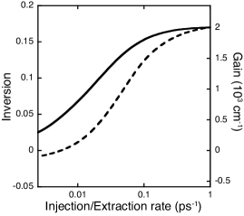
We start by changing and together and keep ps-1 constant. The numerical calculation is done as already described in Sec. IV.2 and the carrier distributions are evolved until a steady-state is reached. The result is shown in Fig. 13 for a lattice temperature of K and K. The inversion curve rises with increasing injection (extraction) rates and goes into saturation around ps-1, which is below the values found for equal rates. Thus, it is possible to reduce the injection (extraction) rate into the source and drain QW, if the extraction rate of the top QW is kept constant at 1 ps-1. In particular, we obtain positive gain for all injection (extraction) rates.
In the next step we vary and keep ps-1 constant. The result is also depicted in Fig. 13 for a lattice temperature of 150 K and 300 K. Gain saturation is reached around ps-1, which was already found in Sec. IV.2. In particular, transparency is reached at similar rates in the two cases. This suggests that the qualitative behavior in figure 8 is dominated by the extraction rate of the top QW.
Finally we vary the ratio between and , while keeping constant. The results are depicted in Fig. 14 for a lattice temperature of 300 K. For 150 K the results are qualitatively similar. If only is varied, the saturation is reached around ps-1 and the gain remains positive for all injection rates. If only is changed, the inversion is more sensitive to this change (note the logarithmic plot), but still reaches comparable values already around an extraction rate of ps-1. Only for a constant ps-1 and a very low extraction rate the gain can be negative, because the carriers are not extracted sufficiently fast from the drain QW. Note that the gain remains positive for all other combinations of these two rates. To sum up, the dependence of the gain on and is similar, and starting from an equal injection (extraction) rate ps-1 the gain is robust against a reduction of or .
For a QCL design it might be important to know the ratio between top and drain QW carrier extraction. A calculation of this ratio in the framework of our model shows that leakage through top QW extraction generally stays around five percent. To avoid a reduction of differential quantum efficiency in a QD based QCL the collector region of the QCL (see section V) should support the relaxation of the extracted top QW carriers into the following source QW.
V Comparison between a QD- and QW-QCL
In our investigation of AlGaAs/InGaAs QW-QD-QW structures as active material for midinfrared lasers, the design of the surrounding heterostructures (e.g. collector region) has not been taken into account, viz., we do not investigate a device model of a QD-QCL. However, the results of the analysis done are transferable to a periodic structure (like a QD-QCL). For that purpose a collector region between the drain QW and the source QW has to be added. In this region the carriers from the top and drain QW are collected and injected into the subsequent source QW. We assume that all carriers extracted from the precedent top and drain QWs are injected into the subsequent source QW, i.e. carrier losses in the collector region are neglected. Under this assumption the steady-state current density through the QD-QCL device can be determined as described in Sec. III.2. In the following we compare our results to those of a QW-QCL investigated in Ref. Harrison1, . Therefore we choose an analogous confinement factor of and a similar device periodicity of nm, which corresponds to a field around 36 kV/cm for our structure. The small-signal modal gain is given by
| (7) |
where nm is the periodicity length of the structure. The other parameters are the same as in Sec. IV.1, see Eq. (6)). Here, we have also included an inhomogeneous broadening of the QD ensemble. While the polarization dephasing determines the homogeneous broadening, the inhomogeneous broadening acts as an effective reduction of the density of QDs that are resonant with the optical field.
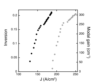
The carrier distributions for variable uniform injection rates are evolved until a steady-state is reached and the steady-state injection current density into the source QW and the steady-state modal gain (calculated from the inversion ) is determined. In Fig. 15 the modal gain versus current density for different injection rates is plotted for a lattice temperature of 150 K and 300 K without inhomogeneous broadening. Qualitatively, a higher current density leads to a higher modal gain. For a lattice temperature of 300 K, a higher current density is needed to obtain the same modal gain. In particular, for a lattice temperature of 150 K and an injection rate of ps-1, a steady-state current density of A cm-2 and an inversion close to saturation of N is reached. For a lattice temperature of 300 K the same inversion is reached for an injection rate of ps-1 and a steady-state current density of A cm-2.
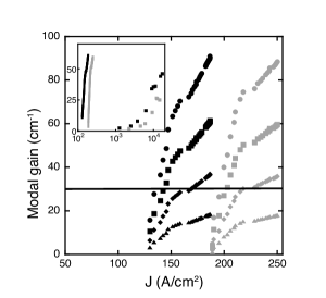
In Fig. 16 the modal gain versus current density for different injection rates is plotted for lattice temperatures of 150 K and 300 K. The inhomogeneous broadening is included via a Gaussian profile with FWHM of 10 meV, 15 meV, 25 meV and 50 meV. The total loss line is chosen in agreement with Ref. Harrison1, as cm-1. It is a summation of the mirror and waveguide losses. An inhomogeneous broadening with a FWHM smaller than 25 meV is necessary to overcome the total losses . For an inhomogeneous broadening with FWHM between 10 meV and 25 meV and a lattice temperature of 150 K a threshold current density around A cm-2 and for a lattice temperature of 300 K a threshold current density around A cm-2 is needed. In comparison to the results obtained for a QW-QCL structure investigated in Ref. Harrison1, (their Fig. 14), which are displayed in the inset of Fig. 16, the threshold current density is approximately 50 times lower in our QD-QCL structure. However, a comparable gain can be only achieved for an inhomogeneous broadening of the QD ensemble that is close to what is achievable by self-organized growth at present. More recent experimental results for QW-QCL devices reach threshold current densities of about kA cm-2. In particular, in Ref. Slivken, a threshold current density as low as has been measured for a device with a smaller total loss and a larger confinement factor than assumed in our calculation. A direct comparison to these more recent experimental devices leads to threshold reduction of roughly a factor of 5.
VI Conclusion
In conclusion, we presented a microscopic calculation for the gain arising from intersubband transitions in QDs in the mid-infrared range. In order to provide a realistic description of how inversion on an electronic intersubband transition in QDs can be achieved, we assumed that a QD layer was sandwiched between a source and a drain QW, and we modeled the carrier injection and extraction into the QWs, respectively. We included a realistic description of the QD electronic structure and a microscopic treatment of electron-phonon and electron-electron scattering. We analyzed two structures, which differed mainly in a separation of the source QW from the QD and top QW. It was found that substantial gain can only be achieved if one allows for direct carrier extraction from the scattering continuum of the QDs, which is only possible if the source QW is separated from the QD and drain as well as the top QW. Only in this case the scattering states above the QD do not become substantially occupied by the injection. If the population of the scattering states is too large, these electrons act as scattering partners for electrons in the localized QD states, and lead to a more efficient relaxation towards the QD ground state, thus decreasing the inversion in the QD. For the optimized structure significant gain is found in the small signal limit as well as beyond the small signal limit up to . For higher field intensities the gain of the QD intersubband transition is depleted. The dependence of the gain versus field intensity can be used as a figure of merit for the performance as gain material in a laser. In addition, the tradeoff between the different injection (extraction) pathways was analyzed and potential leakage pathways were discussed. We found that the rates are dominated by the extraction rate of the top QW and the ratio between top and drain QW carrier extraction is around five percent. Finally, we compared our QD-QCL to a standard QW-QCL device as analyzed in Ref. Harrison1, and more recent experimental results. Slivken The threshold current densities predicted for the QD-QCL structure are reduced in comparison to QW-based designs, but a comparable modal gain for the QW- and QD-QCL structure is possible only for an inhomogeneous broadening of the QD ensemble that is close to what is achievable today.
Acknowledgements.
This work was supported in part by Sandia’s Solid-State Lighting Science Center, an Energy Frontier Research Center (EFRC) funded by the US Department of Energy, Office of Science, Office of Basic Energy Sciences.Appendix A Calculation of the electronic structure and the Coulomb- or carrier-phonon-scattering matrix-elements
The electronic structure consisting of conduction-band QW and QD states is calculated by kp theory. We calculated the one-dimensional envelopes of the QWs and the three-dimensional QD states in a single-band approximation using the software package in Ref. homepage, . The values for material parameters of AlGaAs and InGaAs compounds are taken from Ref. material, . This approach cannot handle the whole system in one “box,” which would yield localized and delocalized eigenfunctions that are orthogonal to each other. Instead, we extend the one-dimensional envelopes of the QWs to three-dimensional QW states
| (8) |
assuming a parabolic conduction band with plane waves as in-plane functions and -independent energy values for the QW states . To describe the combined system we orthogonalize the QW states to the QD states with
| (9) |
where is a normalization constant. The outcome of this are localized and delocalized eigenfunctions that are orthogonal to each other. ortho
For the following explanations its useful to simplify the notation of the band index. Here, we investigate a QD d of the ensemble with electron states embedded in a QW structure consisting of a source-QW S, a top-QW W and a drain-QW D. Especially, in a single-band approximation for the conduction band c where all electron states are spin degenerate, every state in the QD can be labeled by where is a generalized band index, is a QD state index and is the spin index. States in the QWs are labeled by where is a generalized band index for the source-, top- and drain-QW. Thus we introduce the notation with for all states. With this unified index a simplified notation of the carrier-phonon interaction matrix-elements and the carrier-carrier interaction matrix-elements follows.
The electron-electron and electron-phonon scattering contributions are gathered in appendix B. Here, we are concerned with the computation of and . The carrier-carrier interaction matrix-elements are calculated using
| (10) |
where
| (11) | |||
| (12) |
In the numerical implementation of the electron-electron scattering, the Coulomb-matrix elements including the integrals are part of an integral-kernel expression , which is independent of the angle of . For the calculation of , has cylindrical coordinates, because they are well suited for the evaluation of our QW system with embedded QD states.
For QD-QD, QW-QD and QD-QW integrals are calculated numerically because the wave-function overlaps are finite in all three dimensions. QW-QW integrals has to be calculated semi-analytically similar to Ref. Jahnke1, , because the integral components related to the in-plane functions resulting in -functions which has to be included into or as analytical expressions. The Coulombmatrix has to be interpreted by an distinction between different combinations of QW and QD states. More precisely, we distinguish between intra-QW scattering (4 QW states), QW-assisted QD capture/emission (3 QW states), QW-assisted QD scattering (2 QW states paired), pure QD-QW scattering (2 QW states unpaired), QD-assisted QD capture/emission (3 QD states) and intra-QD scattering (4 QD states). Finally, the Coulombmatrix is included into the electron-electron scattering integral-kernel where all integrals over the ’s, i.e. angles, are evaluated.
In the numerical implementation of the electron-phonon scattering, the carrier-phonon interaction matrix-elements are also part of an integral-kernel expression , which is independent of the angle of . Especially, the electron-phonon scattering integral-kernel contains the expression
| (13) |
where is the prefactor of the Froehlich Hamiltonian. We evaluated analog to , because the expressions in resulting from Equ. (13) can be treated comparable to the expressions in resulting from Eq. (10). For the carrier-phonon interaction matrix-elements we can distinguish between intra-QW scattering (2 QW states), phonon-assisted QD capture/emission (1 QW state) and intra-QD scattering (2 QD states).
Appendix B Scattering contributions
We calculate the electron densities for the whole system under investigation dynamically. Thus, electron-phonon and electron-electron scattering terms including both QW- and QD-states. For the analysis of the scattering contributions we distinguish between intra-QW electron scattering, intra-QD electron scattering and QD-QW scattering processes, but summarize the explicit expressions with an unified index. More precisely, we refer to intra-QW electron-electron and electron-phonon scattering as intra-QW electron scattering processes and to intra-QD electron-electron and electron-phonon scattering as intra-QD electron scattering processes. Further, we summarize QW-, QD-, or phonon-assisted QD electron capture/emission, QW-assisted QD-scattering and pure QD-QW scattering and refer to them as QD-QW electron scattering processes. However, for the explicit scattering contributions we use our unified index as introduced in appendix A. A simplified notation of the carrier-phonon interaction matrix-elements and the carrier-carrier interaction matrix-elements follows.
The derivation of the scattering contributions is described in Ref. QDM, . In contrast to Ref. QDM, all coherences are neglected and we assume that only conduction band states are involved in the scattering process. With a generalized notation for the electron densities we obtain for scattering processes due to the carrier-phonon interaction in Markov approximation
| (18) |
where denotes the real part and can be understood as a complex single-particle energy with an energy shift and a damping , i.e., broadening in energy, reflecting a quasi-particle lifetime. This broadening is important for the discrete levels of the QD and includes polaronic effects.
Further we evaluated an expression for scattering processes due to carrier-carrier interaction as described in Ref. QDM, . In contrast to Ref. QDM, again all coherences are neglected and we assume that only conduction band states are involved in the scattering process. We obtain for the carrier-carrier interaction in Markov approximation
| (21) |
References
- (1) C. Gmachl, F. Capasso, D. L. Sivco and A. Y. Cho, Rep. Prog. Phys. 64, 1533-1601 (2001).
- (2) S. Kumar, IEEE J. Sel. Top. Quant. Electronics. 17, 38 (2011).
- (3) Y. Bai, S. Slivken, S. Kuboya, S. R. Darvish, and M. Razeghi, Nature Photonics 4, 99 (2010).
- (4) Y. Yao, A. J. Hoffman, and C. F. Gmachl, Nature Photonics 6, 432 (2012)
- (5) R. C. Iotti, and F. Rossi, Phys. Rev. Lett. 87, 146603 (2001)
- (6) D. Indjin, P. Harrison, R. W. Kelsall, and Z. Ikoni, J. Appl. Phys. 91, 9019 (2002)
- (7) V. D. Jovanovi, D. Indjin, Z. Ikoni, and P. Harrison, Appl. Phys. Lett. 84, 2995 (2004)
- (8) C. A. Evans, V. D. Jovanovic, D. Indjin, Z. Ikonic, and Paul Harrison, IEEE J.Q.E. 42, NO. 9, 859-867 (2006)
- (9) I. Waldmueller, M. C. Wanke, M. Lerttamrab, D. G. Allen, and W. W. Chow, IEEE J.Q.E. 46, NO. 10, 1414-1420 (2010)
- (10) I. Waldmueller, M. C. Wanke, and W. W. Chow, Phys. Rev. Lett. 99, 117401 (2007).
- (11) Y. Bai, S. R. Darvish, S. Slivken, W. Zhang, A. Evans, J. Nguyen, and M. Razeghia, Appl. Phys. Lett. 92, 101105 (2008).
- (12) A. Lyakha, P. Zory, D. Wasserman, G. Shu, C. Gmachl, M. D’Souza, D. Botez, and D. Bour, Appl. Phys. Lett. 90, 141107 (2007).
- (13) L. Diehl, D. Bour, S. Corzine, J. Zhu, G. Hoefler, M. Loncar, M. Troccoli, and F. Capassoa, Appl. Phys. Lett. 88, 201115 (2006).
- (14) R. Koehler , A. Tredicucci, F. Beltram, H. E. Beere, E. H. Linfield, A. G. Davies, D. A. Ritchie, R. C. Iotti, and F. Rossi, Nature 417, 156 (2002).
- (15) J. Faist, F. Capasso, C. Sirtori, D. L. Sivco, J. N. Baillargeon, A. L. Hutchinson, S.-N. G. Chu, and A. Y. Cho, Appl. Phys. Lett. 68, 3680 (1996).
- (16) H. Page, C. Becker, A. Robertson, G. Glastre, V. Ortiz, and C. Sirtori, Appl. Phys. Lett. 78, 3529 (2001).
- (17) R. Colombelli, K. Srinivasan, M. Troccoli, O. Painter, C. F. Gmachl, D. M. Tennant, A. M. Sergent, D. L. Sivco, A. Y. Cho, F. Capasso, Science 302, 1374 (2003).
- (18) H. Benisty, Phys. Rev. B 51, 13281 (1995).
- (19) H. Benisty, C. M. Sotomayor-Torres, and C. Weisbuch, Phys. Rev. B 44, 10945 (1991).
- (20) E. W. Bogaart, J. E. M. Haverkort, T. Mano, T. van Lippen, R. Nötzel, and J. H. Wolter, Phys. Rev. B 72, 195301 (2005).
- (21) D. Smirnov, C. Becker, O. Drachenko, V. V. Rylkov, H. Page, J. Leotin, and C. Sirtori, Phys. Rev. B 66, 121305(R) (2002).
- (22) I. Savic̀, N. Vukmirovic̀, Z. Ikonic̀, D. Indjin, R. W. Kelsall, P. Harrison, and V. Milanovic̀, Phys. Rev. B 76, 165310 (2007).
- (23) V. Liverini , A. Bismuto , L. Nevou , M. Beck , F. Gramm , E. Mueller, and J. Faist, J. Crystal Growth 323, 491 (2011).
- (24) I. A. Dimitriev, R. A. Suris, Physica E 40, 2007 (2008).
- (25) R. Heitz, H. Born, F. Guffarth, O. Stier, A. Schliwa, A. Hoffmann, and D. Bimberg, Phys. Rev. B 64, 241305(R) (2001).
- (26) M. Phillips, H. Wang, Opt. Lett. 28, 831 (2003).
- (27) P.C. Ku, C.J. Chang-Hasnain, and S.L. Chuang, Electron. Lett. 38,1581 (2002).
- (28) D. Pana, E. Toweb, and S. Kennerly, Appl. Phys. Lett. 73, 1937 (1998).
- (29) W. Zhang, H. Lim, M. Taguchi, S. Tsao, B. Movaghar, and M. Razeghia, Appl. Phys. Lett. 86, 191103 (2005).
- (30) F. F. Schrey, L. Rebohle, T. Müller, G. Strasser, K. Unterrainer, D. P. Nguyen, N. Regnault, R. Ferreira, and G. Bastard, Phys. Rev. B 72, 155310 (2005).
- (31) J. Houel, S. Sauvage, P. Boucaud, A. Dazzi, R. Prazeres, F. Glotin, J. M. Ortega, A. Miard, and A. Lemaitre, Phys. Rev. Lett. 99, 217404 (2007).
- (32) G. H. Yeap, S. I. Rybchenko, I. E. Itskevich, and S. K. Haywood, Phys. Rev. B 79, 075305 (2009).
- (33) T. Schwarzl, E. Kaufmann, G. Springholz, K. Koike, T. Hotei, M. Yano, and W. Heiss, Phys. Rev. B 78, 165320 (2008).
- (34) B. H. Hong, S. I. Rybchenko, I. E. Itskevich, S. K. Haywood, C. H. Tan, P. Vines, and M. Hugues, Journal of Applied Physics 111, 033713 (2012).
- (35) N. Ulbrich, J. Bauer, G. Scarpa, R. Boy, D. Schuh, G. Abstreiter, S. Schmult and W. Wegscheider, Appl. Phys. Lett. 83, 1530 (2003).
- (36) D. Wasserman and S. A. Lyon, Appl. Phys. Lett. 81, 2848 (2002).
- (37) S. Anders, L. Rebohle, F. F. Schrey, W. Schrenk, K. Unterrainer, and G. Strasser, Appl. Phys. Lett. 82, 3862 (2003).
- (38) S. Sauvage and P. Boucaud, Appl. Phys. Lett. 88, 063106 (2006).
- (39) S. Krishna, P. Bhattacharya, P.J. McCann and K. Namjou, Electron. Lett. 36, 1550 (2000).
- (40) A. Hochreiner, T. Schwarzl, M. Eibelhuber, W. Heiss, G. Springholz, V. Kolkovsky, G. Karczewski, and T. Wojtowicz, Appl. Phys. Lett. 98, 021106 (2011).
- (41) D. Wasserman, T. Ribaudo, S. A. Lyon, S. K. Lyo, and E. A. Shaner, Appl. Phys. Lett. 94, 061101 (2009).
- (42) S.-W. Chang, S.-L. Chuang, and N. Holonyak, Jr., Phys. Rev. B 70, 125312 (2004)
- (43) Y. I. Mazur, V. G. Dorogan, D. Guzun, E. Marega, Jr., G. J. Salamo, G. G. Tarasov, A. O. Govorov, P. Vasa and C. Lienau, Phys. Rev. B 82, 155413 (2010).
- (44) R. P. Prasankumar, W. W. Chow, J. Urayama, R. S. Attaluri, R. V. Shenoi, S. Krishna, and A. J. Taylor, Appl. Phys. Lett. 96, 031110 (2010).
- (45) W. W. Chow and F. Jahnke, Prog. Quantum Electron. 37, 109 (2013).
- (46) NEXTNANO3 code, released 24-Aug-2004; see www.nextnano.de/nextnano3/
- (47) P. Michler (editor), Single Quantum Dots, Fundamentals, Applications and New Concepts, Springer (2003).
- (48) P. Giannozzi, S. de Gironcoli, P. Pavone, and S. Baroni, Phys. Rev. B 43, 7231 (1991).
- (49) E. A. Muljarov, T. Takagahara, and R. Zimmermann, Phys. Rev. Lett. 95, 177405 (2005).
- (50) S. Michael, W. W. Chow, and H. C. Schneider, Phys. Rev. B 88, 125305 (2013).
- (51) J. Seebeck, T.R. Nielsen, P. Gartner, and F. Jahnke, Phys. Rev. B 71, 125327 (2005).
- (52) M. Lorke, T. R. Nielsen, J. Seebeck, P. Gartner, and F. Jahnke, Phys. Rev. B 73, 085324 (2006).
- (53) S. Michael, Theory of Semiconductor Quantum-Dot Systems: Applications to Slow Light and Laser Gain Materials, Sierke, Goettingen (2010).
- (54) W. W. Chow and S. W. Koch, Semiconductor-Laser Fundamentals, Springer, Berlin (1999).
- (55) H. Lim, W. Zhang, S. Tsao, T. Sills, J. Szafraniec, K. Mi, B. Movaghar, and M. Razeghi, Phys. Rev. B 72, 085332 (2005)
- (56) M. Lorke, J. Seebeck, T. R. Nielsen, P. Gartner, and F. Jahnke, phys. stat. sol. (c) 3, 2393 (2006)
- (57) S. Slivken, A. Evans, W. Zhang, and M. Razeghi, Appl. Phys. Lett. 90, 151115 (2007)
- (58) I. Vurgaftman, J. R. Meyer, and L. R. Ram-Mohan, J. Appl. Phys. 89, 5815 (2001).
- (59) H. C. Schneider, W. W. Chow, and S. W. Koch, Phys. Rev. B 64, 115315 (2001).
- (60) T.R. Nielsen, P. Gartner, and F. Jahnke, Phys. Rev. B 69, 235314 (2004).