Point-contact spectroscopy of the heavy-fermion superconductor CePt3Si
Abstract
Differential resistance spectra ( characteristics) have been measured for point-contacts between the heavy-fermion superconductor (HFS) CePt3Si and a normal metal. Some contacts show a peak at that is characteristic of HFS coexisting with a magnetic order such as UPd2Al3, UNi2Al3 and URu2Si2. The evolution of the peak occurs well above the antiferromagnetic transition temperature 2.2 K, so that the direct relationship with the magnetic transition is questionable. The half-width of the peak seems to reflect the crystal field splitting or the spin-wave gap as observed for the above-mentioned HFSs, possibly suggesting that some common scattering process induces the zero-bias peaks in these materials.
pacs:
74.50.+r, 74.70.Tx, 72.15.QmThe heavy fermion superconductor (HFS) CePt3Si has attracted much attention in recent years[1, 2], since its noncentrosymmetric crystal structure and strong correlation between electrons may lead to the mixing of spin-singlet and spin-triplet superconductivity. The spin triplet superconductivity is supported experimentally by the large upper critical field[1] and the NMR Knight shift[3], while the Hebel-Slichter peak in the nuclear spin-lattice relaxation rate suggests conventional spin-singlet superconductivity[4]. In addition to this duality, the temperature dependence of various physical properties such as thermal conductivity[5] and magnetic penetration depth[6] suggests the line node in the energy gap. A theoretical work that combines and explains all these results has been proposed[7].
Besides unconventional superconductivity, CePt3Si is the first Ce-based heavy fermion superconductor that coexists with an antiferromagnetic order at ambient pressure. The spin structure has been revealed by neutron diffraction measurements[8]. Its complex pressure-temperature phase diagram has been investigated by specific heat[9] and magnetic susceptibility measurements[10], although the correlation between magnetism and superconductivity is still not clear. Since this issue directly relates to which symmetry of superconductivity is favored in this material, it will be useful to investigate how the electronic state is modified through the antiferromagnetic and superconducting transition.
Point-contact spectroscopy, which measures the bias voltage dependence of the differential resistance of the point-contacts, has given fruitful information for both normal and superconducting states of heavy fermion materials[11]. In the normal state, most materials show a minimum of at zero bias and it has been ascribed to the increase in local temperature due to Joule heating. The exceptions that show a zero-bias maximum are URu2Si2, UPd2Al3 and UNi2Al3[11, 12]. It should be noted that these materials show superconductivity that coexists with antiferromagnetism (UPd2Al3[13], UNi2Al3[14]) or so-called ”hidden order”(URu2Si2[15]). It will be interesting to test whether such a spectral property is common to the heavy-fermion superconductors that coexist with a magnetic order.
In this paper, we investigate the point-contact spectroscopy of CePt3Si and report that it also shows a similar structure at zero bias. Possible factors that determine the energy width of the structures are discussed also.
A single crystal of CePt3Si was grown by the Bridgeman method. Details of the process for producing the crystal are provided in previous papers[16, 17]. In the present study, a rectangular piece with edges of about 3 mm was used; point contacts were made on the (100) and (001) faces. Hereafter, the contacts are denoted as and , assuming that the preferred current direction is perpendicular to the surface. Prior to measurements these faces were polished using diamond polish down to a size of 1 m to obtain a mirror-like surface. A Pt needle was gently pressed onto the sample with a commercial piezo-electric actuator (attocube ANPx100) to form a point contact between a superconductor and a normal metal. The position of the contacts were changed using another actuator (attocube ANPz100). These actuators move stepwise by about 100 nm at low temperatures, which enables precise control of the contact resistance and position. The point-contact apparatus was set to the mixing chamber of a dilution refrigerator and cooled down to 80 mK.
The differential resistance of the point contacts was measured by the four-wire method using a system that consists of a current source (Keithley 6221) and a nanovoltmeter (Keithley 2182). The combination of them provides a special pattern of current sweep and is numerically derived; a constant differential current is added to or subtracted from a staircase sweep, and both the differential voltage and the bias voltage are calculated from the voltage measured at each current step. The sign of the bias voltage is referred to the polarity of the needle.

Figure 1 shows the superconducting transition of the CePt3Si crystal used for the present investigation. As the temperature is decreased, the resistance of the bulk CePt3Si shows a gradual decrease, followed by a drop below 80 K, and then becomes zero at 0.6 K. As seen in the inset, a slight change in slope appears at 2.2 K.
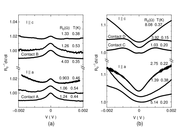
We show in figure 2 spectra taken below for different contacts on (100) and (001) faces. The differential resistance for each contact is normalized by at . For both current directions, two types of spectra have been observed. One type shows a zero-bias peak with a voltage width of 1 mV (figure 2(a)). The other is characterized by a minimum at zero bias with a width varying widely (figure 2(b)). The lack of a clear difference between the - and -axis directions does not necessarily exclude the anisotropy in CePt3Si, since the directionality tends to be lost in point-contact spectroscopy due to the roughness of the surface.

As the temperature is increased, we have observed that both types of structures gradually diminish, but still exist well above , so that they are not attributed to superconductivity. As a typical example, the temperature dependence of the spectra for Contact A in figure 2 (a) is shown in figure 3. The temperature dependence was measured during the warming process from the lowest temperature, and we often encountered an abrupt change in above 3 K, possibly because the boiling of 3He/4He mixture begins and causes the change in the contact condition by vibrations. In figure 3, the spectra after the abrupt change in are also shown by shifting vertically by an appropriate extent. Although the curve shape also changes a little, the peak at zero bias seems to diminish successively and vanish above 4.2 K. The observation of the zero-bias peak above 2.2 K raises the question as to whether the peak structure is ascribed to the antiferromagnetism.
In order to clarify the origin of the peak, we should examine what kind of information the measured differential resistance contains. In the case that CePt3Si and Pt contact through a circular plane of radius , the contact resistance at zero bias is approximately expressed as the sum of Sharvin resistance and Maxwell resistance , as given by
| (1) |
where is the Fermi wave number, k, and is the electrical resistivity of CePt3Si near the contact[18, 19]. The due to Pt resistivity has been neglected, because it is supposed to be small and independent of temperature at low temperatures. The two parts become comparable at a resistance of . If cm[16] is used and a typical metallic 10 nm-1 is assumed, is about 0.02 ; if as seen in the present contacts, is dominant and the data contain intrinsic spectroscopic information. In the actual point contacts, however, near the surface is possibly larger than that of the bulk, and an oxide layer that inhibits a clean metallic contact may be formed on the CePt3Si surface. Consequently the dominant part of resistivity should be judged not only from the value but also from the behaviour of .
As seen in the inset of figure 3, increases as the temperature is lowered. This cannot be explained by the temperature dependence of in the Maxwell resistance, since the resistance of bulk CePt3Si decreases by lowering the temperature, as shown in figure 1. The increase in should be ascribed to and contain some spectroscopic information. Such peak structures have been observed for only a few heavy-fermion systems: point-contact spectroscopy of URu2Si2[11] and scanning tunneling spectroscopy of URu2Si2, UPd2Al3 and UNi2Al3[12]. It should be noted that all these materials including CePt3Si are heavy-fermion superconductors that coexist with an antiferromagnetic order, although for URu2Si2 the order is now regarded as some other type, which is so-called hidden order.
For most of heavy-fermion systems, a minimum in at zero bias is usually observed as seen in figure 2 (b) and is explained by a heating or thermal model; if the inelastic mean free path is much smaller than the contact size , is dominant and the increase in local temperature occurs. In this model, the relation is satisfied, where and are the bath temperature and the Lorenz number, respectively[11]. This leads to an approximate expression (K/mV)(mV), when . Since the largest bias voltage 2mV in figure 2 corresponds to K, the temperature dependence of in figure 1 suggests that the spectra should be V-shaped in the thermal model.
Although some of the spectra are nearly V-shaped in figure 2 (b), the broad maximum at about 1 mV observed for Contacts C and D cannot be explained by the thermal model. Moreover, such a double maximum structure, which resembles the spectra observed in many superconductors[20], cannot be ascribed to superconductivity, since it does not disappear well above as described below. The similarity of the voltage width between the zero-bias peak in figure 2 (a) and the double maximum structure in figure 2 (b) may suggest that the spectra for Contacts C and D also reflect ; the difference in the interface barrier determines whether a peak or a dip appears at zero bias, as observed for superconductors in the BTK theory[21].
As seen in figures 2 and 3, some of the contacts have shown an asymmetry of curves versus : . If this asymmetry has a spectroscopic origin, it will reflect energy-dependent electronic DOS (density of states) around the Fermi level. However, the fact that the asymmetry is remarkable for the contacts following the thermal model in figure 2 (b) and at higher bias voltages in figure 3 suggests that the thermoelectric voltage caused by the increase in temperature at the point contacts is a more likely origin[11], although the details of the Seebeck coefficient of CePt3Si is still not clear.
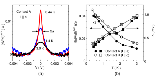
Hereafter, we focus on the zero-bias peak that is common to HFS with a magnetic order. The evolution of the peak structure is examined by extracting the symmetric part from the spectra using the equation
| (2) |
Typical examples of the symmetric part are shown in figure 4(a) for the spectra in figure 3. The peak height is defined as . The half-width of the peak is defined at half-height. The temperature dependence of both properties are given in figure 4(b) for Contact A () and Contact B () in figure 2 (a). For both contacts, decreases with a decrease in temperature. This is in contrast to the behaviour observed for URu2Si2; appears at , slightly increases by lowering the temperature, which is regarded as the growth of the energy gap at the Fermi surface[11].
-
(K) (meV) (meV) URu2Si2 17.5 9.5 9.9 UPd2Al3 14 13 13 UNi2Al3 4.6 10 CePt3Si 2.2 1[8]
Table 1 summarizes the characteristics of heavy-fermion superconductors that show a zero-bias peak. For the U-based materials, two possible interpretations of the peak structure has been proposed. One is a gap opening on the Fermi surface due to spin-density-wave formation in the antiferromagnetic state[11, 12]. The other interpretation is based on the fact that is comparable to the crystal field splitting between the two levels that are connected by a non-zero matrix element; reflects a spin-wave gap determined by .[12]
Although the temperature dependence of the peak for CePt3Si is different from URu2Si2 as described above, in figure 4 (b) is an order of magnitude smaller than for the other U-based materials, suggesting the possible scaling law between and . In addition, is comparable to . It should be noted that the spin-wave gaps derived from heat capacity and resistivity data also have similar values: 2.7 K (0.23 mV) and 1.8 K (0.16 mV), respectively[2]. Although is of the same order of magnitude as various physical properties related to antiferromagnetism in CePt3Si, the lack of a drastic change of the spectra at raises a question about its antiferromagnetic origin. A comprehensive interpretation of the zero-bias peak is left to future study.
As for the spectroscopic evidence of superconductivity, we could not observe it in contrast to the clear unconventional spectra in the normal state, as shown in figure 3. The absence of a superconducting anomaly has also been reported for URu2Si2, especially in high-resistance contacts[22, 23], and ascribed to the normal-conducting layer near the surface of URu2Si2. One possible origin of such a layer is the deformation in the contact region and it probably occurs in CePt3Si as well. Even if such a deformed region becomes superconducting, it will only show a reduced anomaly, which is often characterized by the finite quasiparticle lifetime in the BTK theory[11]. Moreover, the unconventional spectra in the normal state of CePt3Si that grow at lower temperatures and on a lower voltage scale than in URu2Si2 ( K, mV) tend to hide the superconducting anomaly on the scale of the energy gap ( mV), so that the superconducting anomaly has hardly been observed.

The only exception is Contact C in figure 2 (b). Figure 5 shows the temperature dependence of the spectra for Contact C. The double maximum structures at about mV change little within this temperature range. In addition, a small local maximum appears at zero bias below 0.6 K. Such a structure is expected when a superconductor and a normal metal are separated by an interface barrier; the voltage mV where the double minimum appears indicates the superconducting energy gap[21]. This value, however, only gives the lower limit of the gap, since the double maximum structure outside is so steep that it tends to make the minimum appear at lower values. Still, meV is larger than the weak-coupling limit = 0.09 meV with 0.6 K, indicating the strong coupling superconductivity in CePt3Si.
In conclusion, point-contact spectroscopy of CePt3Si has shown a dip or a peak of the differential resistance at zero bias. The dip structure varies from contact to contact, while the peak has a half-width of the order of the crystal field splitting or the spin-wave gap. Such a peak structure is commonly observed for heavy-fermion superconductors that coexist with a magnetic order, although for CePt3Si the peak disappears not at but well above .
References
References
- [1] Bauer E, Hilscher G, Michor H, Paul Ch, Scheidt E W, Gribanov A, Seropegin Yu, Noel H, Sigrist M and Rogl P 2004 Phys. Rev. Lett. 92 027003
- [2] Bauer E, Kaldarar H, Prokofiev A, Royanian E, Amato A, Sereni J, Brämer-Escamilla W and Bonalde I 2007 J. Phys. Soc. Jpn. 76 051009
- [3] Ueda K, Hamamoto K, Kohara T, Motoyama G and Oda Y 2005 Physica B 359-361 374
- [4] Yogi M, Kitaoka Y, Hashimoto S, Yasuda T, Settai R, Matsuda T D, Haga Y, Ōnuki Y, Rogl P and Bauer E 2004 Phys. Rev. Lett. 93 027003
- [5] Izawa K, Kasahara Y, Matsuda Y, Behnia K, Yasuda T, Settai R and Ōnuki Y 2005 Phys. Rev. Lett. 94 197002
- [6] Bonalde I, Brämer-Escamilla W and Bauer E 2005 Phys. Rev. Lett. 94 207002
- [7] Hayashi N, Wakabayashi K, Frigeri P A and Sigrist M 2006 Phys. Rev B 73 092508
- [8] Metoki N, Kaneko K, Matsuda T D, Galatanu A, Takeuchi T, Hashimoto S, Ueda T, Settai R, Ōnuki Y and Bernhoeft N 2004 J. Phys.: Condens. Matter 16 L207
- [9] Tateiwa N, Haga Y, Matsuda T D, Ikeda S, Yasuda T, Takeuchi T, Settai R and Ōnuki Y 2005 J. Phys. Soc. Jpn. 74 1903
- [10] Aoki Y, Sumiyama A, Motoyama G, Oda Y, Settai Y and Ōnuki Y 2007 J. Phys. Soc. Jpn. 76 114708
- [11] Naidyuk Yu G and Yanson I K 1998 J. Phys.: Condens. Matter 10 8905
- [12] Aarts J, Volodin A P, Menovsky A A, Nieuwenhuys G J and Mydosh J A 1994 Europhys. Lett. 26 203
- [13] Geibel C, Schank C, Thies S, Kitazawa H, Bredl C D, Böhm A, Rau M, Grauel A, Caspary R, Helfrich R, Ahlheim U, Weber G and Steglich F 1991 Z. Phys. B 84 1
- [14] Geibel C, Thies S, Kaczorowski D, Mehner A, Grauel A, Seidel B, Ahlheim U, Helfrich R, Petersen K, Bredl C D and Steglich F 1991 Z. Phys. B 83 305
- [15] Palstra T T M, Menovsky A A, van den Berg J, Dirkmaat A J, Kes P H, Nieuwenhuys G J and Mydosh J A 1985 Phys. Rev. Lett. 55 2727
- [16] Yasuda T, Shishido H, Ueda T, Hashimoto S, Settai R, Takeuchi T, Matsuda T D, Haga Y and Ōnuki Y 2004 J. Phys. Soc. Jpn. 73 1657
- [17] Takeuchi T, Hashimoto S, Yasuda T, Shishido H, Ueda T, Yamada M, Obiraki Y, Shiimoto M, Kohara H, Yamamoto T, Sugiyama K, Kindo K, Matsuda T D, Haga Y, Aoki Y, Sato H, Settai R and Ōnuki Y 2004 J. Phys.: Condens. Matter 16 L333
- [18] Wexler G 1966 Proc. Phys. Soc. 89 927
- [19] Gloos K 2000 Phys. Rev. Lett. 85 5257
- [20] Sheet Goutam, Mukhopadhyay S and Raychaudhuri P 2004 Phys. Rev. B 69 134507
- [21] Blonder G E, Tinkham M and Klapwijk T M 1982 Phys. Rev. B 25 4515
- [22] Nowack A, Naidyuk Yu G, Chubov P N, Yanson I K and Menovsky A 1992 Z. Phys. B 88 295
- [23] Hasselbach K, Kirtley J R and Lejay P 1992 Phys. Rev. B 46 5826