Semimetalic graphene in a modulated electric potential
Abstract
The -electronic structure of graphene in the presence of a modulated electric potential is investigated by the tight-binding model. The low-energy electronic properties are strongly affected by the period and field strength. Such a field could modify the energy dispersions, destroy state degeneracy, and induce band-edge states. It should be noted that a modulated electric potential could make semiconducting graphene semimetallic, and that the onset period of such a transition relies on the field strength. There exist infinite Fermi-momentum states in sharply contrast with two crossing points (Dirac points) for graphene without external fields. The finite density of states (DOS) at the Fermi level means that there are free carriers, and, at the same time, the low DOS spectrum exhibits many prominent peaks, mainly owing to the band-edge states.
pacs:
73.20.At, 73.22.-f, 81.05.UwI Introduction
Carbon atoms could form diamond, graphites, carbon nanotubes, C60-related fullerenes, carbon onions, and carbon tori. These systems own special symmetric configurations, and their dimensionalities range from 3D to 0D. These systems are of great interest to community because of the spectacular physical properties to which the unique geometric structures give rise. Recently, a new carbon-based material is discovered by the success in experimental realization of fabricating a single graphene sheet Novoselov et al. (2004); Berger et al. (2004), and immediately this unique 2D system becomes the focus of both theoretical and the experimental researches. One of the unique physical properties of the kind of system, for example, is the observation of an anomalous quantum Hall effect Novoselov et al. (2005), where the plateau of zero Hall conductance is unexpectedly absent. The novel phenomenon of Hall conductivity quantization is attributed to that the dynamics of quasiparticles in graphene is effectively relativistic, contrasting sharply with the conventional integer quantum Hall effect in the regular 2D electron system that are governed by the Schrodinger fermions.
Graphene has a honeycomb crystal structure with two distinct triangular sublattices A and B. This real-space structure corresponds to a triangular lattice in the reciprocal space, which also defines a hexagonal Brioullin zone with two inequivalent corners, and . The unique geometrical configuration of graphene leads to several non-trivial characteristics of its energy spectrum. There exist two identical low-energy bands in the vicinity of the two inequivalent corners, of which each exhibits a linear energy dispersion with conduction and valence bands crossing right at the corner. The highly diminished Fermi surface gives rise to a zero density of states at the Fermi level, so graphene a zero-gap semiconductor.
Studying the behavior of electrons under various kinds of external fields is not only of vital importance for understanding their physical nature of materials but also helpful for designing novel devices or developing applications. Many researches has been conducted on the physical properties of graphene, such as electronic properties Bostwick et al. (2007); Peres et al. (2006a); Partoens and Peeters (2007); Peres et al. (2006b); Partoens and Peeters (2006), transport properties Novoselov et al. (2004); Gusynin and Sharapov (2005); Adam et al. (2007); Jiang et al. (2007); Novoselov et al. (2007); Stauber et al. (2007), optical properties Sadowski et al. (2006, 2007); Deacon et al. (2007); Gusynin et al. (2007a, b); Koshino and Ando (2008), and electronic excitations Guinea (2007); Hwang and Sarma (2007); Wang and Chakraborty (2007). Here we focus on the effects of modulated fields on the electronic properties, an intriguing field of less exploration Matulis and Peeters (2007); Tahir and Sabeeh (2007, 2008); Barbier et al. (2008); Chiu et al. (2008); Ho et al. (2008). The systems for graphene in the modulated fields are not yet realized experimentally; however, the 2D electron gas formed by GaAs/AlGaAs heterojunctions in modulated fields are well-established systems and have been subject of active studies in the past two decadesGerhardts et al. (1989); Messica et al. (1997); Kato et al. (1998, 1999). For the 2D electron gas, there are probably two types of periodic modulations in actual systems. One is an electrostatic modulation and the other is a magnetic-field modulation. The former can be realized by a periodic array of gate electrodes Messica et al. (1997) and the latter by depositing magnetic materials on the surface Kato et al. (1998, 1999). In the case of magnetic modulation, the electronic properties of graphene have been recently studied Chiu et al. (2008); Ho et al. (2008). In this paper, we would like to further investigate the electronic properties of graphene in a modulated electric potential. The tight-binding model is employed to calculate the energy spectrum and the density of states. Both are analysed as functions of the field strength, the period, and the direction by solving the Hamiltonian matrix numerically. In this work, it is shown that semiconducting graphene can be made semimetallic by applying a modulated electric potential. Any finite value of field strength will cause such a transition with a prerequisite that the period of modulated potential is longer enough. However, a qualitative study, recently made by other authors, on the Dirac particles tunneling through a one-dimensional potential barrier predicts that the 2D light-cone structure is still preserved under such a field Barbier et al. (2008). The underlying reason causing the different findings is elaborated in the discussion part.
This paper is organized as follows. The tight-binding Hamiltonian matrix in a periodic electric potential is derived in Sec. II. The main characteristics of the -electronic structures are discussed in Sec. III. Finally, Sec. IV contains concluding remarks.
II Model and Methods: Tight-binding Model
The -electronic structure of graphene is calculated by the tight-binding model within the nearest-neighbor interactions. Given that graphene is a two-dimensional triangular lattice with two-point basis, we construct the -electronic eigenfunction of the system:
| (1) |
where the tight-binding Bloch function () is the superposition of the orbitals from periodic () atoms. The coefficients are obtained by diagonalizing the Hamiltonian matrix in the space spanned by the tight-binding Bloch functions. Moreover, with the two prerequisites that site energies for A and B atoms are the same, and that intra-sublattice hoppings are ignored, we can set . The nonvanishing matrix elements are given by
| (2) |
where eV is the nearest-neighbor hopping integral with being the lattice vector and the atomic orbital. are the vectors connecting a carbon atom to its three nearest neighbors, and they are given by , , and , where is the C-C bond length. , denoting individual hopping process, is then explicitly given by , , and . After specifying the matrix elements, the zero-field Hamiltonian is expressed as the following Hermitian matrix,
| (5) |
The Hamiltonian matrix can be solved analytically, and it generates two energy dispersions represented by . The low-energy spectrum shows symmetry between two valleys (around K and K’), where both have the identical light-cone structure described by the relation , with light velocity and momentum measuring the difference () in wavevector and corner () of the Brioullin zone.
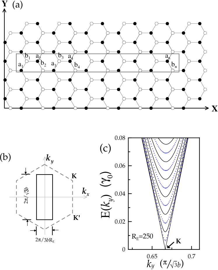
Considering graphene exists in a 1D modulated potential along the armchair direction (), and the potential profile is assumed to take the form with being the field strength. For convenience, the period, , is further designed to be a multiple of , with . In doing so, the periodicity caused by such a field is made commensurate with the crystal potential of graphene itself, which helps define a primitive cell. The rectangular primitive cell is enlarged to include carbon atoms denoted as () with for A(B)-type carbon atoms (Fig. 1(a)). The corresponding rectangular Brioullin zone shrinks to be of the original hexagonal Brioullin zone, and its dimension along the modulated direction () is relatively shorter than the other one (), as shown in Fig. 1(b). The eigenfunction of a system is the superpostion of elements in the basis composed of Bloch functions, , and is represented as
| (6) |
When the period is sufficiently large, the effects of the electric potential on the off-diagonal matrix elements are negligible. Meanwhile, the the diagonal matrix elements would become
| (7) |
where is the total Hamiltonian. In effect, the assumption made above is plausible. The period ( m) in a typical experimental setup is still much longer than the extension of atomic orbital ( ), so the atomic orbital feels approximately a constant potential within its distribution. To facilitate the calculation, the basis functions are further rearranged in a specific sequence to obtain the band Hamiltonian matrix, . The band Hamiltonian matrix of graphene in a modulated electric potential along the armchair direction is written as
| (16) |
with and .
Graphene owns the anisotropic geometry so that the -electronic structure could depend on the modulation direction. When the modulation direction is changed into the zigzag direction (), the diagonal matrix element becomes
| (17) |
In this case, the period is designed as for the same reason mentioned earlier in the armchair case. The corresponding rectangular Brioullin zone also shrinks to be of the original hexagonal Brioullin zone, and its dimension is characterized by along the zigzag direction and along the other. The Hamiltonian matrix can be easily constructed in a similar way to that in the armchair case (not shown here).
In the following discussion, we will consider the situation that the actual modulation period is about submicron length, which corresponds to . This involves a process of diagonalizing a very large Hamiltonian matrix, and it is solved numerically to obtain the energy bands. Due to the resulting unoccupied conduction bands () and occupied valence bands () being symmetric about the Fermi level (), we only discuss the former.
III Electronic Properties
Before presenting the results under a modulated electric potential, a brief review of the main features of low-energy bands of the zero-field system is made. As mentioned earlier, the low-energy band structure has a linear energy dispersion around K or K’ of the hexagon. However, it is not convenient to compare directly with the coming case when a modulated field is present, because they are presented in different Brillouin zones. To treat them on an equal footing, the unit cell of the zero-field system is chosen to be identical to the primitive cell of the system in a modulated potential. That is, if the modulated field has a period , the unit cell is chosen to be times its primitive cell. In this way, all electronic states in the hexagonal Brillouin zone are folded into a rectangular one. Notice that such a folding method guarantees not to change any features of the original band structure. Figure 1(c) shows the -dependence of the low-energy spectrum at for (black solid lines) and (blue dotted lines). There exists a nondegenerate 1D linear band and doubly degenerate 1D parabolic bands for , while they are purely doubly degenerate 1D parabolic bands for . The evolution of bands from to fills the states between them, which reflects the 2D characteristic of the light-cone structure. (This energy spectrum corresponds to one of the two valleys containing the Dirac point K now located at and .) Above the Dirac point, there exists a local minima for each 1D parabolic band. Notice that these points should not be considered as band-edge states. For these states, the -dependent energy dispersion is linear with nonzero first derivative, so they cannot be treated as critical points. The band structure is in all respects the same as one before folding the zone. Although this alternative representation of band structure somewhat complicates the explanation, it is advantageous for the following discussion to compare the zero-field system and the system in a modulated electric potential.
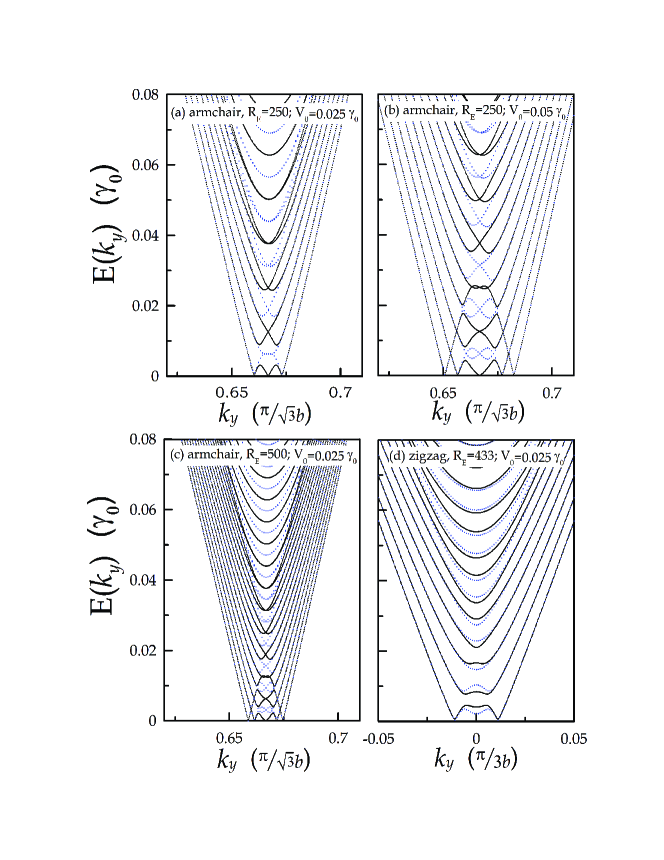
A modulated electric potential has a strong effect on the energy dispersions, state degeneracy, and band-edge states. The -dependent conduction bands for (black solid lines) and (blue dotted lines) are shown in Fig. 2(a) for the modulated electric potential along the armchair direction with the period ( nm) and the strength . Moreover, the potential mainly affects the structure of some low 1D bands. The original doubly degenerate parabolic bands are split. The energy dispersions around the are strongly deformed, and induce several band-edge states which are saddle points in the energy-momentum space. These band-edge states always appear in pairs at two sides of , and two band-edge states is each pair might have small energy difference. Far away from the , the spectrum is almost linear for the dependence, while it becomes dispersionless for the dependence, which can been seen in Fig. 2(a) where the bands for and have identical dispersion. It is important to note that there exist more Fermi momentum states ’s. The energy dispersions near ’s are linear for the -dependence, while they are completely flat for the -dependence. The dispersionless feature means that the number of the Fermi-momentum states is infinite, which sharply contrasts with the original two Fermi-momentum states or Dirac points in zero-field graphene. Besides, the non-zero measure of the Fermi surface indicates finite value of the DOS at the Fermi level.
The aforementioned features might rely on the strength, period, and direction of a modulated electric potential. The modulation effects are even enhanced when field is strengthened, illustrated in the Fig. 2(b). When the strength increases, more low 1D bands are affected. The energy bands are further deformed, and more band-edge states are created. In addition, the number of Fermi-momentum states increases almost linearly with the field strength. For the case in Fig. 2(b), the number of Fermi-momentum states is approximately double that in Fig. 2(a). The modulation period can also affect the numbers of band-edge states and Fermi-momentum states, as shown in Fig. 2(c). When the period increases, more band-edge states are created. The number of Fermi-momentum states remains almost unchanged in the long-period regime, whereas there is a drastic change in the small-period regime. The former can be understood by taking into consideration both the accompanying reduced length and increased ’s associated with different ’s in accordance with the increasing period, while the latter will be discussed later by calculating the density of states at the Fermi level. The low-energy bands are, on the other hand, not sensitive to the direction of a modulated electric potential. Figure 2(d), for example, presents the bands for the potential modulated along the zigzag direction.
The essential features of electronic structure are directly reflected on the density of states, and defined as
| (18) |
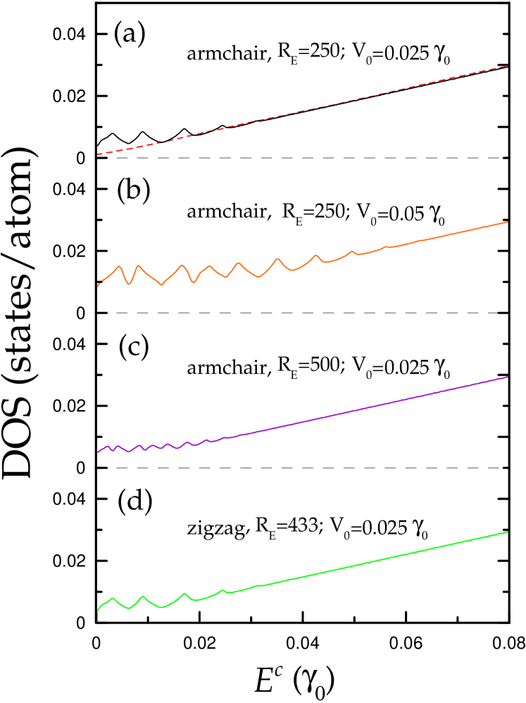
Because of the linear energy dispersion, the low-frequency DOS without fields is proportional to , as shown by dotted line in Fig. 3(a), and it has no special structures. The vanishing DOS at indicates that graphene is a zero-gap semiconductor. A modulated electric potential can lead to many prominent peaks and a finite DOS at (Figs. 3(a)-3(d)). The peak structures come from the band-edge states of parabolic bands (Figs. 2(a)-2(d)). The frequency, number, and height of peaks are sensitive to the changes in the field strength and period. The DOS at the Fermi level means that there are free carriers, so graphene becomes a semimetal in the presence of a modulated electric field. The value of DOS at grows as the field strength increases (Figs. 3(a) and 3(b)). However, it does not change significantly as the period is varied (Fig. 3(c)). Moreover, the low-frequency DOS is unaltered when the modulation direction changes (Fig. 3(d)), which reflects the isotropic symmetry of graphene in low-energy spectrum.
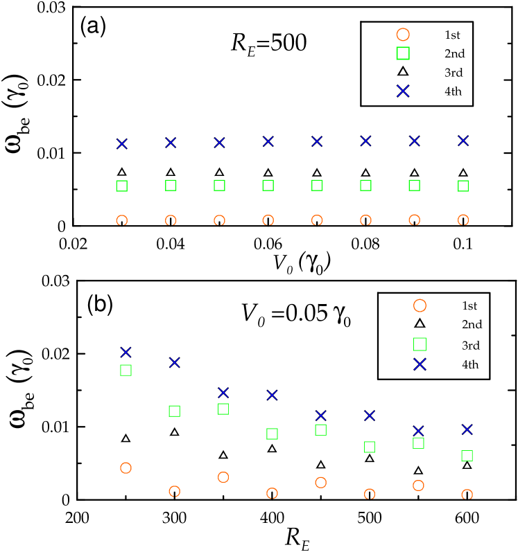
The singularities in the DOS might cause special structures in some physical quantities, for example, giving rise to the strong absorption peaks in optical measurement, so it is worthy to investigate their properties in detail. The peak height, number and frequency are dominated by the strength and period of the potential (Figs. 3(a)-3(c)). The peak height is enhanced by the increasing strength, whereas it is reduced by the increasing period. The peak number is increased by both the increasing strength and period. The relations between of the peak frequency () and the field condition are elaborated through examining the first four prominent peaks, as shown in the Fig. 4(a) for the strength dependence and Fig. 4(b) for the period dependence. From these, it is observed that the peak frequency weakly depends on the strength, while declines and presents somewhat oscillatory behavior as the period increases.
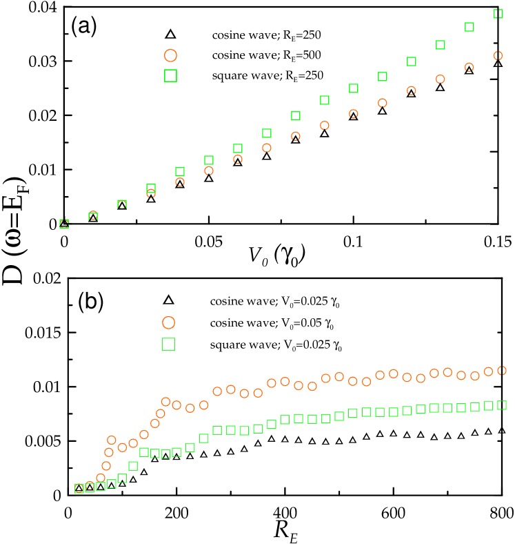
The relationship between the DOS at and the field strength and that between the field strength and the period deserve a closer investigation. Referring to Fig. 5(a), shows a nearly linear variation with the field strength. This relation just reflects the fact that the number of Fermi-momentum states is approximately proportional to field strength. On the other hand, the period dependence of exhibits different features in short- and long-period regimes, as shown in Fig. 5(b). The two regions are distinguished by a threshold period , which happens at for ( black triangles in Fig. 5(b)) and becomes shorter as the field strength gets stronger ( red circles in Fig. 5(b)). For , remains zero as increases from zero, which implies that the 2D light-cone structure is not affected at such a short period. As is increased to cross , quickly grows and saturates to a definite value, with some fluctuations in the long-period regime. If one consider a realistic experimental system, the typical modulation period will be about submicron or even longer. The then would fall into the long-period regime, so its value does not change significantly as the period is varied. Therefore, this feature should be very robust even there exist some inevitable period fluctuations coming from processing devices or experimental setups.
These interesting features, including field induced band-edge states and the semimetallic behavior of graphene, caused by the modulated electric potential are the main results in this work. Nevertheless, the semimetallic behavior, the most important feature, was not obtained in a recent study Barbier et al. (2008). The study considered graphene subjected to a square-wave like modulated potential, concluding that the 2D light-cone structure is still preserved. Although the conclusion seems to contradict with our results given here, a in-depth examination shows that this is not the case. The main discrepancy lies in the fact that the modulation period used (20 nm ) in their calculation is too short to achieve the threshold (), so that the semimetallic behavior was not observed. To clarify this point, the dependence of on the field strength and the modulation period for a square-wave potential is calculated here, as shown by green squares in Figs. 5(a) and 5(b) respectively. in Fig. 5(a) exhibits a linear relation with the field strength, which is similar to the cosine-wave potential. The threshold period in this case is (Fig. 5(b)), which is close to that in the cosine-wave potential. As a result, from Fig. 5(b), it self-evidently explains the reason why the semimetallic behavior is not observed by other authors solely because that taken in their calculation is less than .
IV Concluding Remarks
In summary, the tight-binding model is used to investigate the effects of a modulated electric potential on the -electronic structure of graphene. The low-energy electronic properties are mainly dominated by field strength and period. However, they are not sensitive to the field direction, which is due to the isotropy of the original low-energy bands. A modulated electric potential drastically changes the energy dispersions, state degeneracy, and band-edge states. The density of states exhibits a lot of prominent peaks. These structures are mainly determined by the energy dispersions and the band-edge states. Notice that there are infinite Fermi-momentum states. The finite DOS at the Fermi level indicates the existence of free carriers. The semiconducting graphene becomes semimetallic by applying a modulated electric potential, as long as the period surpasses a threshold period (). Different nature of the low-energy excitations for graphene in the presence of a modulated potential is expected to give rise intriguing physical properties. For instance, the free electrons are expected to cause the low-frequency plasmon. The theoretical predictions could be tested by the experimental measurements on the energy loss spectra.
Acknowledgements.
This work was supported by NSC and NCTS of Taiwan, under the Grant Nos. NSC 96-2112-M-006-002.References
- Novoselov et al. (2004) K. S. Novoselov, A. K. Geim, S. V. Morozov, D. Jiang, Y. Zhang, S. V. Dubonos, I. V. Grigorieva, and A. A. Firsov, Science 306, 666 (2004).
- Berger et al. (2004) C. Berger, Z. M. Song, T. B. Li, X. B. Li, A. Y. Ogbazghi, R. Feng, Z. T. Dai, A. N. Marchenkov, E. H. Conrad, P. N. First, et al., J. Phys. Chem. B 108, 19912 (2004).
- Novoselov et al. (2005) K. S. Novoselov, A. K. Geim, S. V. Morozov, D. Jiang, M. I. Katsnelson, I. V. Grigorieva, S. V. Dubonos, and A. A. Firsov, Nature 438, 197 (2005).
- Bostwick et al. (2007) A. Bostwick, T. Ohta, T. Seyller, K. Horn, and E. Rotenberg, Nat. Phys. 3, 36 (2007).
- Peres et al. (2006a) N. M. R. Peres, F. Guinea, and A. H. C. Neto, Phys. Rev. B Condens. Matter. Mater. Phys. 73, 125411 (2006a).
- Partoens and Peeters (2007) B. Partoens and F. M. Peeters, Phys. Rev. B Condens. Matter. Mater. Phys. 75, 193402 (2007).
- Peres et al. (2006b) N. M. R. Peres, F. Guinea, and A. H. C. Neto, Ann. Phys. 321, 1559 (2006b).
- Partoens and Peeters (2006) B. Partoens and F. M. Peeters, Phys. Rev. B Condens. Matter. Mater. Phys. 74, 075404 (2006).
- Gusynin and Sharapov (2005) V. P. Gusynin and S. G. Sharapov, Phys. Rev. Lett. 95, 146801 (2005).
- Adam et al. (2007) S. Adam, E. H. Hwang, V. M. Galitski, and S. Das Sarma, Proc. Natl. Acad. Sci. USA 104, 18392 (2007).
- Jiang et al. (2007) Z. Jiang, Y. Zhang, H. L. Stormer, and P. Kim, Phys. Rev. Lett. 99, 106802 (2007).
- Novoselov et al. (2007) K. S. Novoselov, Z. Jiang, Y. Zhang, S. V. Morozov, H. L. Stormer, U. Zeitler, J. C. Maan, G. S. Boebinger, P. Kim, and A. K. Geim, Science 315, 1379 (2007).
- Stauber et al. (2007) T. Stauber, N. M. R. Peres, and F. Guinea, Phys. Rev. B Condens. Matter. Mater. Phys. 76, 205423 (2007).
- Sadowski et al. (2006) M. L. Sadowski, G. Martinez, M. Potemski, C. Berger, and W. A. de Heer, Phys. Rev. Lett. 97, 266405 (2006).
- Sadowski et al. (2007) M. L. Sadowski, G. Martinez, M. Potemski, C. Berger, and W. A. de Heer, Solid State Commun. 143, 123 (2007).
- Deacon et al. (2007) R. S. Deacon, K. C. Chuang, R. J. Nicholas, K. S. Novoselov, and A. K. Geim, Phys. Rev. B Condens. Matter. Mater. Phys. 76, 081406 (2007).
- Gusynin et al. (2007a) V. P. Gusynin, S. G. Sharapov, and J. P. Carbotte, Phys. Rev. Lett. 98, 157402 (2007a).
- Gusynin et al. (2007b) V. P. Gusynin, S. G. Sharapov, and J. P. Carbotte, J. Phys. Condens. Matter 19, 026222 (2007b).
- Koshino and Ando (2008) M. Koshino and T. Ando, Phys. Rev. B Condens. Matter. Mater. Phys. 77, 115313 (2008).
- Guinea (2007) F. Guinea, Phys. Rev. B Condens. Matter. Mater. Phys. 75, 235433 (2007).
- Hwang and Sarma (2007) E. H. Hwang and S. D. Sarma, Phys. Rev. B Condens. Matter. Mater. Phys. 75, 205418 (2007).
- Wang and Chakraborty (2007) X.-F. Wang and T. Chakraborty, Phys. Rev. B Condens. Matter. Mater. Phys. 75, 033408 (2007).
- Matulis and Peeters (2007) A. Matulis and F. M. Peeters, Phys. Rev. B Condens. Matter. Mater. Phys. 75, 125429 (2007).
- Tahir and Sabeeh (2007) M. Tahir and K. Sabeeh, Phys. Rev. B Condens. Matter. Mater. Phys. 76, 195416 (2007).
- Tahir and Sabeeh (2008) M. Tahir and K. Sabeeh, Phys. Rev. B Condens. Matter. Mater. Phys. 77, 195421 (2008).
- Barbier et al. (2008) M. Barbier, F. M. Peeters, P. Vasilopoulos, and J. J. M. Pereira, Phys. Rev. B Condens. Matter. Mater. Phys. 77, 115446 (2008).
- Chiu et al. (2008) Y. H. Chiu, Y. H. Lai, J. H. Ho, D. S. Chuu, and M. F. Lin, Phys. Rev. B Condens. Matter. Mater. Phys. 77, 045407 (2008).
- Ho et al. (2008) J. H. Ho, Y. H. Lai, Y. H. Chiu, and M. F. Lin, Nanotechnology 19, 035712 (2008).
- Gerhardts et al. (1989) R. R. Gerhardts, D. Weiss, and K. v. Klitzing, Phys. Rev. Lett. 62, 1173 (1989).
- Messica et al. (1997) A. Messica, A. Soibel, U. Meirav, A. Stern, H. Shtrikman, V. Umansky, and D. Mahalu, Phys. Rev. Lett. 78, 705 (1997).
- Kato et al. (1998) M. Kato, A. Endo, S. Katsumoto, and Y. Iye, Phys. Rev. B 58, 4876 (1998).
- Kato et al. (1999) M. Kato, A. Endo, M. Sakairi, S. Katsumoto, and Y. Iye, J. Phys. Soc. Jpn. 68, 1492 (1999).