Detecting THz current fluctuations in a quantum point contact
using a nanowire quantum dot
Abstract
We use a nanowire quantum dot to probe high-frequency current fluctuations in a nearby quantum point contact. The fluctuations drive charge transitions in the quantum dot, which are measured in real-time with single-electron detection techniques. The quantum point contact (GaAs) and the quantum dot (InAs) are fabricated in different material systems, which indicates that the interactions are mediated by photons rather than phonons. The large energy scales of the nanowire quantum dot allow radiation detection in the long-wavelength infrared regime.
Charge detection with single-electron precision provides a highly-sensitive method for probing properties of mesoscopic structures. If the detector bandwidth is larger than the timescale of the tunneling electrons, single-electron transitions may be detected in real-time. This allows a wealth of experiments to be performed, like investigating single-spin dynamics Elzerman et al. (2004), probing interactions between charge carriers in the system Gustavsson et al. (2006a) or measuring extremely small currents Bylander et al. (2005); Fujisawa et al. (2006); Gustavsson et al. (2008). The quantum point contact (QPC) is a convenient detector capable of resolving single electrons Field et al. (1993). Recently, it has been shown that the QPC not only serves as a measurement device but also induces back-action on the measured system Onac et al. (2006); Khrapai et al. (2006); Gustavsson et al. (2007). The concepts of detector and measured system can therefore be turned around, allowing a mesoscopic device like a quantum dot (QD) to be used to detect current fluctuations in the QPC at GHz frequencies Aguado and Kouwenhoven (2000).
In this work we investigate a system consisting of a QPC defined in a GaAs two-dimensional electron gas (2DEG) coupled to an InAs nanowire QD. We first show how to optimize the charge sensitivity when using the QPC as single-electron detector. Afterwards, the system is tuned to a configuration where electron tunneling is blocked due to Coulomb blockade. With increased QPC voltage bias we detect charge transitions in the QD driven by current fluctuations in the QPC. The fact that the QPC and the QD are fabricated in different material systems makes it unlikely that the interactions are mediated by phonons Khrapai et al. (2006). Instead, we attribute the charge transitions to absorption of photons emitted from the QPC Aguado and Kouwenhoven (2000); Gustavsson et al. (2007); Zakka-Bajjani et al. (2007).
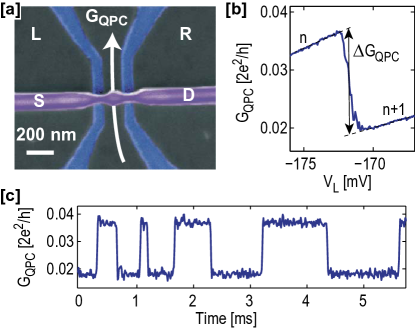
Figure 1(a) shows a scanning electron microscope (SEM) image of the device used in these experiments. An InAs nanowire is deposited on top of a shallow (37 nm) AlGaAs/GaAs heterostructure based two-dimensional electron gas (2DEG). The QPC is defined by etched trenches, which separate the QPC from the rest of the 2DEG. The parts of the 2DEG marked by L and R are used as in-plane gates. The horizontal object in the figure is the nanowire lying on top of the surface, electrically isolated from the QPC. The QD in the nanowire and the QPC in the underlying 2DEG are defined in a single etching step using patterned electron beam resist as an etch mask. The technique ensures perfect alignment between the two devices. Details of the fabrication procedure can be found in Ref. Shorubalko et al., 2008. The electron population of the QD is tuned by applying voltages to the gates L and R. When changing gate voltages, we keep the QPC potential fixed by applying a compensation voltage to the 2DEG connected to both sides of the QPC. All measurements presented here were performed at an electron temperature of .
I Charge detection with a quantum point contact
Figure 1(b) shows a measurement of the QPC conductance as a function of voltage on gate L. The gate voltage tunes both the QPC transmission as well as the electron population on the QD. The measurement was performed without any bias voltage applied to the QD and with the drain lead of the QD pinched off. At , the electrochemical potential of the QD shifts below the Fermi levels of the source lead and an electron may tunnel onto the QD. This gives a decrease of the QPC conductance corresponding to the change of the charge population on the QD. The curve in Fig. 1(b) shows the average QPC conductance giving the time-averaged QD population. By performing a time-resolved measurement, electron tunneling can be detected in real-time. This is visualized in Fig. 1(c), where the measured QPC conductance fluctuates between the two levels corresponding to and electrons on the QD. Transitions between the levels occur on a millisecond timescale, which provides a direct measurement of the tunnel coupling between the QD and the source lead Schleser et al. (2004). By analyzing the time intervals between transitions, the rates for electrons tunneling into or out of the QD can be determined separately Gustavsson et al. (2006b).
Next, we investigate the best regime for operating the QPC as a charge detector. The conductance of a QPC depends strongly on the confinement potential . When operating the QPC in the region between pinch-off and the first plateau , a small perturbation leads to a large change in conductance . If a QD is placed in close vicinity to the QPC, we expect a fluctuation in the QD charge population to shift the QPC potential and thus give rise to a measurable change in QPC conductance. A figure of merit for using the QPC as a charge detector is then
| (1) |
The first factor describes how the conductance changes with confinement potential, which depends strongly on the operating point of the QPC. The second factor describes the electrostatic coupling between the QD and the QPC and is essentially a geometric property of the system.
The performance of the charge detector depends strongly on the operating point of the QPC. The best sensitivity for a device of given geometry is expected when the QPC is tuned to the steepest part of the conductance curve. This corresponds to maximizing the factor in Eq. (1). In Fig. 2(a) we plot the conductance change for one electron entering the QD versus QPC conductance, in the range between pinch-off and the first conductance plateau (). The change is maximal around but stays fairly constant over a range from 0.3 to . The dashed line in Fig. 2(a) shows the numerical derivative of with respect to gate voltage. The maximal value of coincides well with the steepest part of the QPC conductance curve. The inset in the figure shows how the conductance changes as a function of gate voltage.
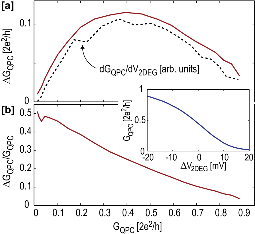
In Fig. 2(b), we plot the relative change in conductance for the same set of data. The relative change increases monotonically with decreasing conductance, reaching above 50% at . The relative change in QPC conductance in this particular device is extraordinarily large compared to top-gate defined structures, where is typically around one percent for the addition of one electron on the QD Vandersypen et al. (2004); Reilly et al. (2007). We attribute the large sensitivity to the close distance between the QD and QPC (, due to the vertical arrangement of the QD and QPC) and to the absence of metallic gates on the heterostructure surface, which reduces screening.
The results of Fig. 2 indicate that it may be preferable to operate the charge detector close to pinch-off, where the relative change in conductance is maximized. The quantity relevant for optimal detector performance in the experiment is the signal-to-noise (S/N) ratio between the change in conductance and the noise level of the QPC conductance measurement. We measure the conductance by applying a fixed bias voltage across the QPC and monitoring the current. In the linear response regime, both the average current and the change in current for one electron on the QD () scale linearly with applied bias. The noise in the setup is dominated by the voltage noise of the amplifier, which is essentially independent of the QPC operating point and the applied bias in the region of voltages discussed here. The S/N thus scale directly with
| (2) |
In practice the maximal usable QPC current is limited by effects like heating or emission of radiation which can influence the measured system. If we consider limiting the current, we see from Eq. (2) that the highest S/N is reached for the maximal value of at . However, this operation point requires a large voltage bias to be applied to the QPC. If the QPC bias is larger than the single-particle level spacing of the QD, the current in the QPC may drive transitions in the QD and thus exert a back-action on the measured device Gustavsson et al. (2007) (see next section). Therefore, a better approach is to limit the QPC voltage. Here, the best S/N is obtained when optimizing rather than and operating the QPC close to . The sensitivity of the QPC together with the bandwidth of the measurement circuit allows a detection time of around Gustavsson et al. (2008). The tunneling rates presented in the following were extracted taking the finite detector time into account Naaman and Aumentado (2006).
II Excitations driven by the quantum point contact
In this section we study QD transitions driven by current fluctuations in the QPC. Such excitations were already studied for QDs and QPCs defined in a GaAs 2DEG Onac et al. (2006); Khrapai et al. (2006); Gustavsson et al. (2007). From those experiments, it was not clear how energy was mediated between the systems. The nanowire sample investigated here is conceptionally different because the QD and the QPC are fabricated in different material systems. This allows us to make a statement about the physical processes involved in transmitting energy between the QD and the QPC. Since the two structures sit in separate crystals with different lattice constants and given that the systems hardly touch each other, we can assume that phonons only play a minor role as a coupling mechanism. Instead, we assume the QD transitions to be driven by radiation emitted from the QPC Aguado and Kouwenhoven (2000). Another advantage of the nanowire structure compared to GaAs systems is that the QD energy scales are an order of magnitude larger compared to QDs formed in a GaAs 2DEG. This allows us to investigate radiation at several , reaching into the long-wavelength infrared regime.
We first discuss the QD configuration used for probing the radiation of the QPC. Since the QD level spectrum is not tunable, we can only drive transitions at fixed frequencies corresponding to excited states in the QD Onac et al. (2006). Figure 3(a) shows the level configuration of the system, with the QD electrochemical potential below the Fermi level of the leads. The tunneling barriers are highly asymmetric, with the barrier connecting the QD to the drain lead being almost completely pinched off. We do not apply any bias voltage to the QD. The system is in Coulomb blockade, but by absorbing a photon the QD may be put into an excited state with electrochemical potential above the Fermi energy of the leads. From here, the electron may leave to the source contact, the QD is refilled and the cycle may be repeated.
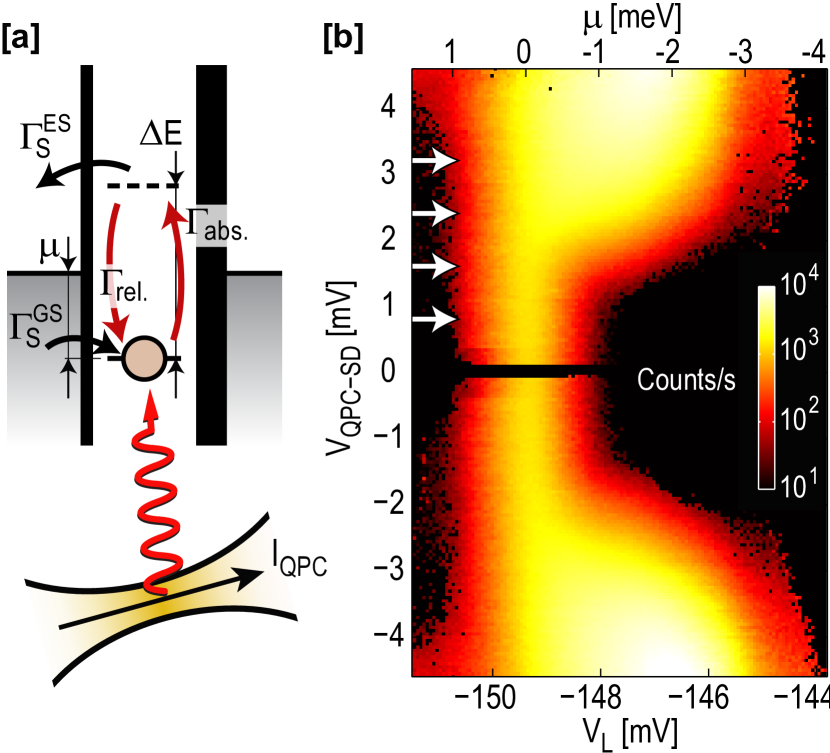
In Fig. 3(b) we plot the electron count rate versus QD potential and QPC bias. The peak at is due to equilibrium fluctuations between the QD and the source contact, with the width set by the electron temperature in the lead. As the QPC bias is increased above , a shoulder appears in the region of . This is consistent with the picture in Fig. 3(a); we need to apply a QPC bias larger than the single-level spacing for the photon-assisted tunneling to become possible. The width of the shoulder is set by and is therefore expected to be independent of QPC bias; we will see later in this section that the apparent smearing of the features in Fig. 3(b) are due to temperature and tuning of the tunneling rates. The picture is symmetric with respect to , meaning that the emission and absorption processes do not depend on the direction of the QPC current. The lack of data points around are due to the fact that the low QPC bias prevents the operation of the QPC as a charge detector. Due to the asymmetric coupling of the QD to the source and drain lead, we could not make a direct confirmation of the existence of an excited state with using finite bias spectroscopy. However, the value is consistent with excited states found in Coulomb diamond measurements in regimes where the tunnel barriers are more symmetric Gustavsson et al. (2008).
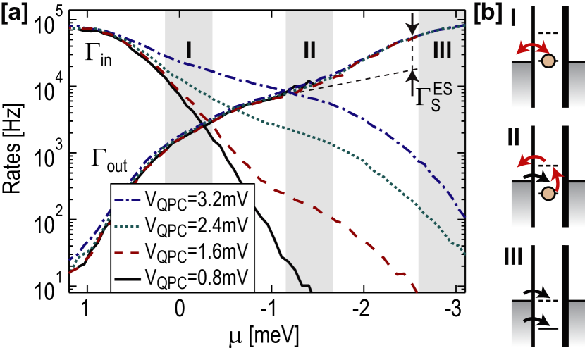
Figure 4(a) shows the separate rates for electrons tunneling into and out of the QD at horizontal cross-sections of Fig. 3(b), measured at four different QPC bias voltages [marked by arrows in Fig. 3(b)]. Around the resonance [, case I in Fig. 4], the tunneling is due to equilibrium fluctuations and the rates for tunneling into and out of the QD are roughly equal. By lowering the electrochemical potential the rate for electrons leaving the QD first falls off exponentially due to the thermal distribution of the electrons in the lead. Continuing to case II of Fig. 4, we come into the regime of QD excitations. Here, the rate is directly related to the absorption process sketched in Fig. 3(a), while the rate corresponds to the refilling of an electron from the lead. Consequently, shows a strong QPC bias dependence, while stays roughly constant.
In case III, the excited state goes below the Fermi level of the source lead and the absorption rate drops quickly. At the same time, increases as the refilling of an electron into the QD may occur through either the ground state or the excited state. This provides a way to determine the tunnel coupling between the source contact and the excited state in the QD (). From the data in Fig. 4(a), we estimate . The change of tunnel coupling with gate voltage makes the exact determination of difficult, the value given here should only be considered as a rough estimate.
The tunneling rates within the region of photon-assisted tunneling are strongly depending on gate voltage. Similar effects have been investigated in 2DEG QDs, where the tunneling rate of a barrier was shown to depend exponentially on gate voltage due to tuning of the effective barrier height MacLean et al. (2007). A difference of our sample compared to 2DEG QDs concerns the properties of the electronic states in the leads. For GaAs QDs, the leads consist of a two-dimensional electron gas where the ideal density of states (DOS) is independent of energy. For the nanowire QD, the leads are also parts of the nanowire and the corresponding electron DOS may show strong variations with energy due to the quasi-one dimensionality and finite length of the wire. Within the region of photon-assisted tunneling in Fig. 4(a), we shift the electrochemical potential of the QD and thereby change the energy of the tunneling electrons relative to the Fermi level in the lead. The measured tunneling rates could therefore show variations due to changes in the DOS in the lead.
However, the behavior seen in region II of Fig. 4(a) is not compatible with the effects discussed in the previous paragraph. The rate is directly related to the tunnel coupling between the source lead and the QD ground state, while the rate depends on the coupling between source and the excited state in the QD. For arguments based on barrier tuning and varying electron DOS, we would expect both and to change in the same way with gate voltage. This is in disagreement with the results of Fig. 4(a); increases while decreases with gate voltage. Instead, we speculate that the observed behavior may be due to non-resonant processes involving energy relaxation in the leads. Focusing on the energy level configuration pictured in Fig. 3(a), we see that there are a large number of occupied states in the lead with energy higher than the electrochemical potential of the QD. Elastic tunneling into the QD can only occur for electrons with energy equal to the electrochemical potential of the QD, but electrons at higher energy may contribute to the measured rate in terms of processes involving relaxation. As we lower , the number of initial states available for the inelastic processes increase and would therefore explain the increase in with decreased . Inelastic tunneling is also possible for electrons leaving the QD excited state to empty states in the lead. Here, the number of empty states available for the inelastic processes goes down when the QD potential is lowered. This is in agreement with the measured decrease in with decreased .
III QPC bias dependence
Next, we investigate how the QPC bias influences the efficiency of the photon absorption process. For this purpose we apply a rate-equation model similar to that used for investigating QPC-driven excitations in double QDs Gustavsson et al. (2007). The model consists of three states, corresponding to the QD being empty, populated with an electron in the ground state, or populated with an electron in the excited state. We write down the master equation for the occupation probabilities of the three states
| (3) |
Here, is the absorption rate and is the relaxation rate of the QD. The rates are visualized in Fig. 3(a). The charge detection technique can only probe rates for electrons entering or leaving the QD. These rates are found from the steady-state solution of Eq. (3):
| (4) |
In GaAs QDs, the charge relaxation process occurs on a timescale of Fujisawa et al. (2002). Similar rates are expected for nanowire QDs. Therefore, we assume and estimate the behavior of in the limit of weak absorption (). Here, Eq. (4) simplifies to
| (5) |
Under these conditions the measured rate is expected to scale linearly with the absorption rate. Assuming the excitations to be driven by fluctuations in the QPC current, we can combine Eq. (5) with the QPC emission spectrum Aguado and Kouwenhoven (2000),
| (6) | |||||
where is the QPC transmission coefficient and the electron temperature in the QPC leads. Note that Eq. (6) only gives the proportionality between and ; to make quantitative predictions for the absorption rate one needs to determine the overlap between the ground and the excited state. For a double QD, this coupling can be extracted from charge localization measurements DiCarlo et al. (2004). However, it is not as straightforward to estimate the overlap for single-QD excitations. One would need to know the shape of the wavefunctions for the different QD states, which is not known.
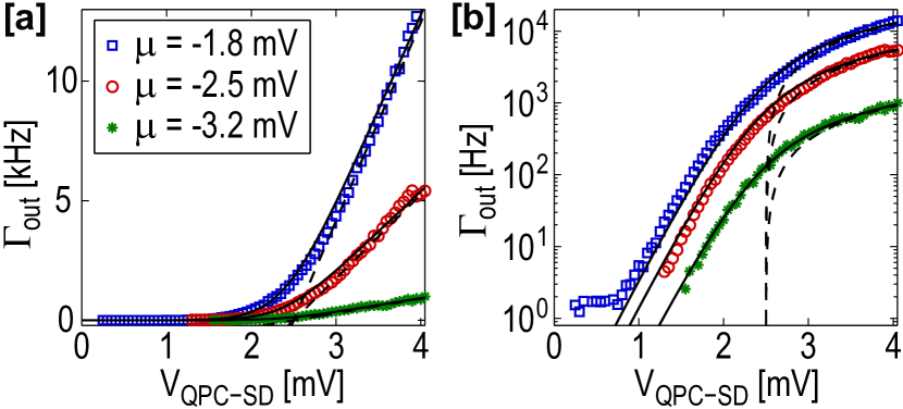
In Fig. 5 we plot the measured tunneling rate related to absorption versus bias on the QPC, measured for three different electrochemical potentials of the QD. The traces correspond to vertical cross-sections for positive in Fig. 3(b). Figure 5(a) shows the rates plotted on a linear scale; the rates taken at all three positions increase linearly with QPC bias as soon as . The solid lines are fits to Eq. (6) with and assuming to be the same for all three traces. As described in the previous section, we attribute the difference in slope for the three cases to changes in effective tunnel coupling with gate voltage [see Fig. 4(a)]. Figure 5(b) shows the same data plotted on a logarithmic scale. Here, we see a clear exponential decay for ; this is due to the thermal distribution of electrons in the QPC Zakka-Bajjani et al. (2007). The dashed lines in Fig. 5 show the rates expected for the case of zero temperature. The weak but non-zero count rate occurring at low QPC bias voltages () for the data taken at is due to non-photon induced thermal fluctuations between the QD ground state and the lead.
To quantify the efficiency of the absorption process we compare the rates and using Eq. (5). Due to the strong change of with gate voltage, we can only make a quantitative comparison between and in the region where we are able to determine (around ). This corresponds to the circles in Fig. 5. For this data set, the measured rate goes up to around for , so that we still have . This confirms that we are in a regime of weak absorption where the relative population of the excited state is much smaller than the population of the ground state. Note that the same is most likely true also for the data sets taken at and in Fig. 5; however, we can not make a quantitative comparison with since we do not have an independent measurement of for those regions.
IV Changing the QPC operating point
In this section, we modify the operating point of the QPC to check how this influences properties of the emitted radiation. Since we use the same QPC both for emitting radiation and for performing charge detection, it is not possible to operate the device at the plateaus where the conductance is fully quantized. However, we could tune the QPC conductance in a region between while still being able to detect the tunneling electrons.
In Fig. 6(a) we plot the electron count rate at the photon-absorption shoulder versus change in . Figure 6(b) shows how the QPC conductance changes with gate voltage within the region of interest. Compensation voltages were applied to the gates L and R in order to keep the QD potential fixed while sweeping . The data was taken with fixed to make the photon absorption process possible. This bias is still lower than the characteristic sub-band spacing of the QPC, which is around . The strong peak at the top of Fig. 6(a) () corresponds to equilibrium fluctuations between the QD and the source lead. In the region of photon-assisted tunneling [marked by the arrow in Fig. 6(a)], the shoulder appears with increasing QPC conductance. Going above , the strength of tunneling at the position of the shoulder decays slightly.
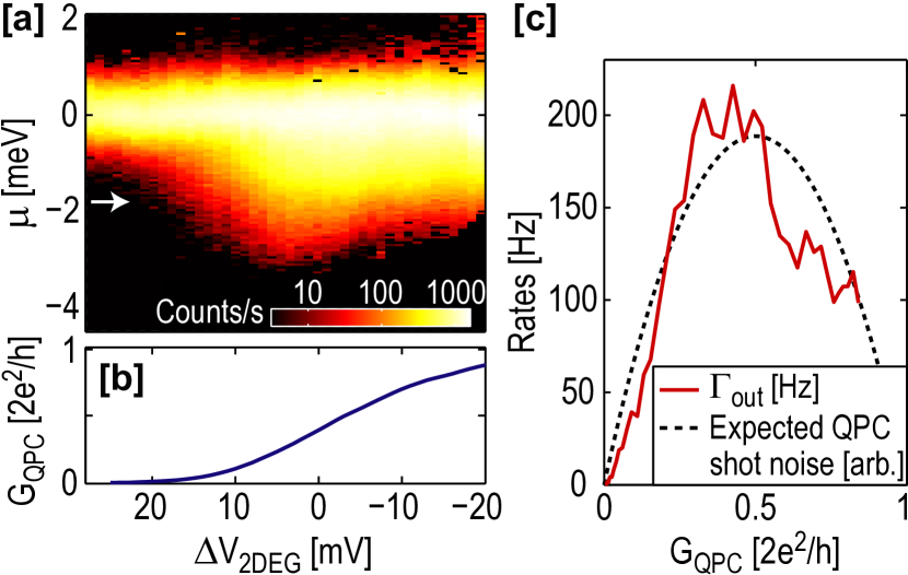
Assuming that the shoulder appears because of radiation emitted from shot noise fluctuations in the QPC current, we expect the measured absorption rate to depend on the transmission of the QPC. From Eq. (6) we see that the emission spectrum scales with , where is the transmission coefficient of the channel. In Fig. 6(c) we plot the rate related to the absorption process, measured at [position of the arrow Fig. 6(a)]. The dashed line shows the emission expected from the QPC, . For low , the measured rate follows the expected emission spectrum reasonably well, with a maximum around .
Still, the measured curve shows deviations compared to the predicted behavior. Suppression of noise close to has been reported Roche et al. (2004); DiCarlo et al. (2006) to be related to 0.7 anomaly Thomas et al. (1996). There are indications of the 0.7 anomaly also in our sample, but we believe the deviations in the measured noise spectrum are more likely to originate from an increase in background charge fluctuations triggered by the QPC current. At large QPC currents (), the noise in the system increases with . This can not be attributed to the intrinsic QPC shot noise but is rather due to fluctuations of trapped charges driven by the high QPC current. The QD is thus placed in an environment of fluctuating potentials, which may lead to QD transitions. The strength of such transitions depends strongly on the number of fluctuators in the neighborhood of the QD Pioda et al. (2007). The charge traps also influence the count rate in the regime of tunneling due to equilibrium fluctuations [peak at in Fig. 6(a)]. For (), the peak is considerably wider than for . Again, this can be attributed to a fluctuating potential at the location of the QD.
To minimize the influence of the charge traps, one would prefer to decrease and operate the QPC at lower current levels. For the configuration used in Fig. 6 (), the QPC current reaches values above at . However, can not be made too small; we need to make sure that is on the same order of magnitude as the level spacing , otherwise the QPC will not emit radiation in the right frequency range. The above discussion only concerns a measurement of the emission properties of the QPC. When using the device to probe radiation of an external source, the QPC can be operated at much lower bias voltages.
To summarize, we have used time-resolved charge detection techniques to investigate the influence of current flow in a near-by QPC to the electron population in nanowire QD. Since the QD and the QPC are fabricated in different material systems, we conclude that phonons can only play a minor role for a transferring energy between the structures. Instead, we attribute the charge to absorption of photons emitted from the quantum point contact. The large energy scales of the nanowire QD allows detection of radiation at a frequency of , thus reaching into the long-wavelength infrared regime. This is an order of magnitude larger than energy scales reachable with GaAs QDs Gustavsson et al. (2007).
References
- Elzerman et al. (2004) J. M. Elzerman, R. Hanson, L. H. Willems van Beveren, B. Witkamp, L. M. K. Vandersypen, and L. P. Kouwenhoven, Nature 430, 431 (2004).
- Gustavsson et al. (2006a) S. Gustavsson, R. Leturcq, B. Simovic, R. Schleser, T. Ihn, P. Studerus, K. Ensslin, D. C. Driscoll, and A. C. Gossard, Phys. Rev. Lett. 96, 076605 (2006a).
- Bylander et al. (2005) J. Bylander, T. Duty, and P. Delsing, Nature 434, 361 (2005).
- Fujisawa et al. (2006) T. Fujisawa, T. Hayashi, R. Tomita, and Y. Hirayama, Science 312, 1634 (2006).
- Gustavsson et al. (2008) S. Gustavsson, I. Shorubalko, R. Leturcq, S. Schön, and K. Ensslin, Appl. Phys. Lett. 92, 152101 (2008).
- Field et al. (1993) M. Field, C. G. Smith, M. Pepper, D. A. Ritchie, J. E. F. Frost, G. A. C. Jones, and D. G. Hasko, Phys. Rev. Lett. 70, 1311 (1993).
- Onac et al. (2006) E. Onac, F. Balestro, L. H. W. van Beveren, U. Hartmann, Y. V. Nazarov, and L. P. Kouwenhoven, Phys. Rev. Lett. 96, 176601 (2006).
- Khrapai et al. (2006) V. S. Khrapai, S. Ludwig, J. P. Kotthaus, H. P. Tranitz, and W. Wegscheider, Phys. Rev. Lett. 97, 176803 (2006).
- Gustavsson et al. (2007) S. Gustavsson, M. Studer, R. Leturcq, T. Ihn, K. Ensslin, D. C. Driscoll, and A. C. Gossard, Phys. Rev. Lett. 99, 206804 (2007).
- Aguado and Kouwenhoven (2000) R. Aguado and L. P. Kouwenhoven, Phys. Rev. Lett. 84, 001986 (2000).
- Zakka-Bajjani et al. (2007) E. Zakka-Bajjani, J. Ségala, F. Portier, P. Roche, D. C. Glattli, A. Cavanna, and Y. Jin, Phys. Rev. Lett. 99, 236803 (2007).
- Shorubalko et al. (2008) I. Shorubalko, R. Leturcq, A. Pfund, D. Tyndall, R. Krischek, S. Schön, and K. Ensslin, Nano Letters 8, 382 (2008).
- Schleser et al. (2004) R. Schleser, E. Ruh, T. Ihn, K. Ensslin, D. C. Driscoll, and A. C. Gossard, Appl. Phys. Lett. 85, 2005 (2004).
- Gustavsson et al. (2006b) S. Gustavsson, R. Leturcq, B. Simovic, R. Schleser, P. Studerus, T. Ihn, K. Ensslin, D. C. Driscoll, and A. C. Gossard, Phys. Rev. B 74, 195305 (2006b).
- Vandersypen et al. (2004) L. M. K. Vandersypen, J. M. Elzerman, R. N. Schouten, L. H. Willems van Beveren, R. Hanson, and L. P. Kouwenhoven, Appl. Phys. Lett. 85, 4394 (2004).
- Reilly et al. (2007) D. J. Reilly, C. M. Marcus, M. P. Hanson, and A. C. Gossard, Appl. Phys. Lett. 91, 162101 (2007).
- Naaman and Aumentado (2006) O. Naaman and J. Aumentado, Phys. Rev. Lett. 96, 100201 (2006).
- MacLean et al. (2007) K. MacLean, S. Amasha, I. P. Radu, D. M. Zumbühl, M. A. Kastner, M. P. Hanson, and A. C. Gossard, Phys. Rev. Lett. 98, 036802 (2007).
- Fujisawa et al. (2002) T. Fujisawa, D. G. Austing, Y. Tokura, Y. Hirayama, and S. Tarucha, Nature 419, 278 (2002).
- DiCarlo et al. (2004) L. DiCarlo, H. J. Lynch, A. C. Johnson, L. I. Childress, K. Crockett, C. M. Marcus, M. P. Hanson, and A. C. Gossard, Phys. Rev. Lett. 92, 226801 (2004).
- Roche et al. (2004) P. Roche, J. Ségala, D. C. Glattli, J. T. Nicholls, M. Pepper, A. C. Graham, K. J. Thomas, M. Y. Simmons, and D. A. Ritchie, Phys. Rev. Lett. 93, 116602 (2004).
- DiCarlo et al. (2006) L. DiCarlo, Y. Zhang, D. T. McClure, D. J. Reilly, C. M. Marcus, L. N. Pfeiffer, and K. W. West, Phys. Rev. Lett. 97, 036810 (2006).
- Thomas et al. (1996) K. J. Thomas, J. T. Nicholls, M. Y. Simmons, M. Pepper, D. R. Mace, and D. A. Ritchie, Phys. Rev. Lett. 77, 135 (1996).
- Pioda et al. (2007) A. Pioda, S. Kičin, D. Brunner, T. Ihn, M. Sigrist, K. Ensslin, M. Reinwald, and W. Wegscheider, Phys. Rev. B 75, 045433 (2007).