theDOIsuffix \VolumeXX \Issue1 \Month01 \Year2007 \pagespan1 \Receiveddate23 September 2007 \Reviseddate7 December 2007 \Accepteddate10 December 2007
Laterally coupled and field-induced quantum Hall systems
Abstract.
A quantum Hall system which is divided into two laterally coupled subsystems by means of a tunneling barrier exhibits a complex Landau level dispersion. Magnetotunneling spectroscopy is employed to investigate the small energy gaps which separate subsequent Landau bands. The control on the Fermi level permits to trace the anticrossings for varying magnetic fields. The band structure calculation predicts a magnetic shift of the band gaps on the scale of the cyclotron energy. This effect is confirmed experimentally by a displacement of the conductance peaks on the axis of the filling factor. Tunneling centers within the barrier are responsible for quantum interferences between opposite edge channels. Due to the disorder potential, the corresponding Aharonov-Bohm interferometers generate additional long-period and irregular conductance features. In the regime of strong localization, conductance fluctuations occur at small magnetic fields before the onset of the regular Landau oscillations. The Landau dispersion is obtained by a dedicated algorithm which solves the Schrödinger equation exactly for a single electron residing in a quantum Hall system with an arbitrary unidirectional, threefold staircase potential.
keywords:
Quantum Hall line junction, Aharonov-Bohm effect, Landau band structure.pacs Mathematics Subject Classification:
02.60.Lj, 61.72.Hh, 73.21.Ac, 73.43.Jn, 73.43.Qt1. Introduction
In the presence of a perpendicular magnetic field, the quasi-free charge carriers of a two-dimensional electron system (2DES) condense in equidistant and numerously degenerated Landau levels [1]. Variations of the electrostatic potential locally shift the degeneracy and, therefore, cause the formation of Landau bands. The bending of the Landau dispersion at the edge of a 2DES is discussed thoroughly in the literature [2, 3] as it is the key for the understanding of the quantum Hall effect [4]. If the lateral extension of a 2DES is limited electrostatically or by the physical edge of the underlying (lithographically defined) structure, the Landau bands rise on a length scale which substantially exceeds the magnetic length. However, if the confining barrier is fabricated by means of epitaxy, namely, by the technique of cleaved-edge overgrowth [5], the realization of a sharp edge potential becomes possible. The corresponding edge channels are then located at distances on the order of the magnetic length [6].
In this paper, we report on the magnetotunneling spectroscopy between two quantum Hall systems which are separated by an atomically precise potential barrier within a GaAs/AlGaAs heterostructure. The width of the barrier amounts to 52 Å, i.e. it falls always below the magnetic length. In the vicinity of the barrier, a complex Landau band structure exists which can be described in the case of weak coupling as a superposition of the mirror-inverted dispersions of both subsystems. The degeneracy at the crossings is lifted by small Landau band gaps [7]. The tunneling current through the structure becomes maximum when the Fermi level coincides with one of these anticrossings [8]. The conductance is additionally determined by random tunneling centers in the barrier which are responsible for quantum interferences between opposite edge channels [9, 10].
[t]
![[Uncaptioned image]](/html/0709.3625/assets/x1.png) \vchcaptiona)
Sample design (not to scale) and measurement setup. b) Landau
dispersion for two strongly coupled electron systems. Edge channels
marked with a circle (square) belong to the left (right) 2DES and
contain electrons which propagate in the negative (positive)
-direction.
\vchcaptiona)
Sample design (not to scale) and measurement setup. b) Landau
dispersion for two strongly coupled electron systems. Edge channels
marked with a circle (square) belong to the left (right) 2DES and
contain electrons which propagate in the negative (positive)
-direction.
While the electron systems of our structure are field-induced by means of a gate electrode, cf. Fig. 1a, a former experiment by Kang et al. is based on modulation-doped electron films [8]. A fixed electron density implies that a certain Landau band gap coincides with the Fermi level only for a small range of the magnetic field. In contrast, a sample design with a gate electrode allows to investigate a particular band gap at different magnetic fields provided that the Fermi level is adjusted in a suitable way. In order to probe the same anticrossing for different barrier widths, it is, therefore, not necessary to prepare several samples as the effective shape of the barrier (in units of the magnetic length and the cyclotron energy ) can simply be varied by the magnetic field. Carrying out measurements for different electron densities with the same sample is also indispensable if quantum interferences are investigated which depend on the random configuration of tunneling centers within the barrier. Another effect can be observed just with a single sample, namely, the small magnetic shift of the Landau band gaps on the scale of the cyclotron energy which would otherwise be perturbed by the unavoidable fluctuations between successive growth processes.
All effects discussed in this paper depend basically on the shape of the Landau band structure at the tunneling barrier (Fig. 1b). For weakly coupled electron systems, Ho has calculated the energy dispersion by using an approximation approach [7]. Though the result reflects the actual dispersion very well, the gap positions differ noticeably from the findings of a complete quantum mechanical calculation if a fine energy resolution is relevant as for our experiment [11, 12]. Instead of combining the dispersions of both subsystems, Takagaki and Ploog have developed a tight-binding model which is not only applicable for weakly, but also for strongly coupled electron systems [13]. The tunneling barrier is thereby represented by a reduced hopping amplitude between two simulation grid lines. Since the effective shape of the barrier is not explicitly considered in this model, the latter is inappropriate to make accurate predictions on the gap position in dependence of the magnetic field.
The Landau dispersion which is necessary for the interpretation of the obtained experimental data has been calculated exactly by solving the single-electron Schrödinger equation. Since the potential term in the Hamiltonian is given by a superposition of the parabolic magnetic confinement potential and the piecewise constant conduction band offset of the intrinsic semiconductor heterostructure, the problem is generally closely related to the linear quantum harmonic oscillator. The analytic solution becomes possible with an ansatz for the wave function which is composed of parabolic cylinder functions. For calculating the energy eigenstates, we have developed a dedicated algorithm which numerically solves the continuity conditions at the heterojunctions. It is generally applicable to all systems which consist of up to three regions of constant potential. Hence, this method yields the Landau dispersion for systems with either a rectangular barrier (biased or not) or a potential well (quantum wire) [14].
This article is organized as follows: The sample structure and the corresponding Landau dispersion are introduced in the next two sections. The subject of Sec. 4 consists of two different tunneling models which are the basis for the understanding of the Landau oscillations and simultaneously occurring conductance fluctuations. In Sec. 5 we discuss a method for determining the electron density from magnetotunneling measurements. The comparison of the conductance traces with the Landau band structure is carried out in Sec. 6 where the focus lies on the magnetic shift of the anticrossings. Section 7 deals with Aharonov-Bohm oscillations at the first conductance peak on the scale of the filling factor. Conductance fluctuations which appear at low magnetic fields are finally discussed in Sec. 8.
2. Experiment
For a quantitative investigation of the energy dispersion in dependence of the magnetic field, it is necessary to have both a well-defined tunneling barrier and electron systems of variable density. The molecular beam epitaxy (MBE) allows the fabrication of GaAs/AlGaAs interfaces with a roughness which is as low as one monolayer. For low-dimensional quantum systems like ours, one commonly needs a sharp potential modulation not just in one, but in two directions of space. For this purpose, Pfeiffer et al. have developed the cleaved-edge overgrowth (CEO) method which allows to grow subsequently two layer sequences at right angles to another [5, 15]. With this technique, the sample structure of Fig. 1a can be realized. It contains two laterally adjacent electron systems which reside in the layers of the first growth step and are induced by means of a gate electrode which is fabricated during the second MBE step.
The source and drain contacts of the heterostructure consist of GaAs layers which are silicon-doped to with thicknesses of 500 and 1100 nm, respectively. The quantum region is composed of a 52 Å thick barrier and two embedding layers of intrinsic GaAs (each 2 m). After the first growth step, the wafer is discharged from the MBE machine and chemically polished to a thickness of 80 to 100 m by means of a bromine methanol solution. The wafer is then cleaved into small pieces which are scratched at a certain position and transferred into the growth chamber again. Immediately after breaking the samples in-situ, the freshly exposed cleavage planes are overgrown with 100 nm of . The barrier region is followed by a 200 nm thick layer of -GaAs with an electron density of . It acts as the gate electrode. By etching a mesa, the buried source contact is exposed. The samples are divided into stripes where each piece contains a 500 m long section of the cleavage plane. Ohmic contacts on the -layers are realized with indium droplets. These are deposited by a soldering iron and subsequently alloyed into the crystal at about 360∘C.
If the active region of a CEO sample is accessed via -layers of the (001) growth step, the occurrence of bulk leakage currents is generally possible [16]. In the case of our structure, the leakage current flows apart from the coupled electron systems through the 4 m thick intrinsic region. In the (001) cross-section of the heterostructure, the induced 2DESs account only for about 1/100,000 of the total area. In order to prevent that conductance oscillations in the quantum region cannot be measured against the background of the bulk leakage current, the aluminum content in the tunneling barrier has to be sufficiently high. Thus the sample design of Fig. 1a allows only Landau band gaps which are considerably smaller than the cyclotron energy. Since for such a dispersion the number of opposite edge states with significant overlap is small in comparison to the low-barrier case which is exemplarily shown in Fig. 1b, this coupling regime is denoted here as weak—independently from the absolute tunneling resistance.
The quality of the indium contacts and of the tunneling barrier is revealed by the two-point I-V-curves of Fig. 2a: Both pairs of junctions on the source and drain contact layers show a perfect ohmic behavior. The ratio of their reciprocal resistance coincides with the thickness ratio of the underlying -contact layers. According to the - curve DS, which represents the leakage current between source and drain for a vanishing gate voltage, the bulk resistance amounts at least 21 k for applied voltages below 10 mV. Therefore, magnetotransport measurements can be carried out with AC voltages which are small enough so that the bulk resistance always exceeds the resistance of the induced electron systems.
[t]
![[Uncaptioned image]](/html/0709.3625/assets/x2.png) \vchcaptiona)
Two-point current-voltage (-) traces for three different
combinations of the source (S) and drain (D) contacts. The bulk
leakage current DS (black curves) is shown both on a linear and
logarithmic scale. b) Magnetotunneling measurements for different
gate voltages at 400 mK.
\vchcaptiona)
Two-point current-voltage (-) traces for three different
combinations of the source (S) and drain (D) contacts. The bulk
leakage current DS (black curves) is shown both on a linear and
logarithmic scale. b) Magnetotunneling measurements for different
gate voltages at 400 mK.
The magnetotransport properties of the quantum region have been investigated by means of lock-in technique. The corresponding circuit is shown in Fig. 1a. In spite of the four-point contact geometry, the active region is effectively accessible only via two leads, namely, the extended -layers of the first growth step. This fact prevents a direct determination of the charge carrier density by standard methods like Shubnikov-de Haas or (quantum) Hall measurements. The coupled electron systems have been studied by applying an AC voltage of via a high-impedance resistor . This setup ensures a practically constant current of . A quasistatic measurement is enabled by a low AC frequency of 17 Hz. All measurements have been carried out within a He system which provides temperatures down to 350 mK.
The resistance traces shown in Fig. 2b in dependence of the magnetic field bear some resemblance to the Shubnikov-de Haas effect. In the following, the prominent long-period resistance oscillations are called Landau oscillations as they originate from the periodic coincidence of the Fermi level with the Landau band gaps. Other magnetotransport features are two different types of conductance fluctuations which appear respectively at low field strengths () and in the range of the rightmost resistance minimum (in Fig. 2b best observable for ). For the understanding of all phenomena, it is necessary to know the Landau band structure at the tunneling barrier quantitatively.
3. Landau band structure
Provided that the electrostatic potential of a two-dimensional Hall system is constant, the energy levels of the charge carriers are given by the solutions of the quantum harmonic oscillator [1]. Close to potential variations, the degeneracy of the Landau levels is lifted so that they form dispersive bands. The particular Landau bands increase monotonically for electrons approaching the confinement potential of a 2DES [3, 17]. In the vicinity of a tunneling barrier, the Landau dispersion shows an oscillating structure which is calculated in the following. With regard to the conduction band shape of the GaAs/AlGaAs/GaAs heterostructure, the treatment is restricted to electron systems which are unidirectionally modulated by three regions of constant potential. The uniform potential within each region makes a representation of the energy eigenfunctions by parabolic cylinder functions possible. Besides, the constraint concerning the number of heterojunctions keeps the equation system which results from the continuity conditions solvable. For a system with a single potential discontinuity, one has to determine only the energy eigenvalue which can be done by means of a standard solution method. A sample structure with two heterojunctions already requires a dedicated solution algorithm for the simultaneous calculation of both the energy eigenvalue and a characteristic mixing parameter. For the analytic and numerical details we refer to Refs. [12] and [14].
The Schrödinger equation which describes the whole quantum region is solved in the scope of the effective mass approximation. For the GaAs layers and the AlGaAs barrier, we use the same effective mass . The aluminum content of the potential barrier corresponds to a conduction band offset of with respect to GaAs [18]. As the barrier height is a multiple of the cyclotron energy , the probability density for electrons at typical magnetic fields is very low inside the AlGaAs material. Consequently, the assumption of a constant effective mass throughout the whole structure is a rather good approximation. For strongly coupled electron systems, however, the difference concerning both the cyclotron energy and the cyclotron radius becomes absolutely relevant [14].
If the conduction band offset is assumed to vary just along the -axis, i.e. in the direction of the first growth step, the Schrödinger equation for a single electron subjected to a magnetic field reads
| (1) |
For electrons propagating parallel to the tunneling barrier and perpendicular to , it is appropriate to use the Landau gauge . This definition of the vector potential implies a wave function which represents a localized state in the - and a plane wave in the -direction:
| (2) |
The integer , 1, 2, is the Landau band index, and stands for the angular wavenumber which determines the wavelength along the -direction. The extension of the system is contained in the ansatz of Eq. (2) for the purpose of normalization. The -dependent component describes a bound state. By using Eq. (2) and the magnetic length , the Schrödinger equation transforms to
| (3) |
The elimination of the -coordinate reduces the partial differential equation (1) to an ordinary differential equation which now solely determines the localized state .
The -quadratic term of the Hamiltonian represents the magnetic confinement potential which is given by a parabola centered at . Only for bulk states, which are not influenced by potential variations, the quantity is always identical to the quantum mechanical expectation value of the electron location. If resides, e.g., within an infinitely high potential step, the probability density vanishes at and the center of mass deviates from this location. In the semiclassical picture, the variable stands for the center of the skipping orbits of electrons propagating along a barrier. Therefore, the parameter is commonly called guiding center. While dispersion relations are generally plotted against the wavenumber , the close connection between the guiding center and the actual location of the electron often gives reasons to use as the abscissa in plots of the Landau band structure. This enables a direct comparison between the dispersion and the potential landscape even when substantially differs from the actual electron position.
[t]
![[Uncaptioned image]](/html/0709.3625/assets/x3.png) \vchcaptiona)
Normalized wave functions for bulk states with . The solid
parabola represents the magnetic confinement potential in units
of . The broken lines enclose regions with
, 0.99,
and 0.999, respectively. b) The graph illustrates the behavior of
for a which approaches an integer from higher or
lower values. The signed numbers denote the difference to
.
\vchcaptiona)
Normalized wave functions for bulk states with . The solid
parabola represents the magnetic confinement potential in units
of . The broken lines enclose regions with
, 0.99,
and 0.999, respectively. b) The graph illustrates the behavior of
for a which approaches an integer from higher or
lower values. The signed numbers denote the difference to
.
Electrons which occupy bulk states are described by wave functions which are already converged to zero at the next potential variation. For these electrons, the term may be neglected in Eq. (3) which then becomes identical to the Schrödinger equation for a quantum harmonic oscillator. Therefore, in regions where the conduction band is flat, the potential in the Hamiltonian is—except for a constant—completely determined by the effect of the Lorentz force:
| (4) |
The last term contains with a dimensionless variable which is used in the following in place of . Bulk electrons which are bound within the parabolic confinement potential occupy the equidistant energy levels . The corresponding wave functions are given by the Hermite functions: . From Fig. 3a it follows that the extension of the wave functions is approximately limited by the parabola . In particular, about 90 of all electrons reside within the interval . Hence, one can deduce a cyclotron radius of which is in fact the half extension of the wave function. For electrons with a guiding center which is located at a distance of about or less in respect of a potential step, the quantum harmonic oscillator is no longer a good approximation.
For solving the Schrödinger equation (3) separately for each region of constant potential, it is necessary to admit for a moment the most general solution which also includes diverging eigenfunctions. By using the dimensionless variables and , where the latter is defined according to , the Schrödinger equation transforms to the Weber differential equation. For the -th region of constant potential , we get
| (5) |
The corresponding two-dimensional solution space is spanned by the linearly independent parabolic cylinder functions [19]. If both outermost intervals are of the same material—in our case GaAs—, it is appropriate to set which leads to the total wave function
| (6) |
The parameters denote the positions of both heterojunctions which are assumed to be located symmetrically around the origin. As illustrated in Fig. 3b, the function diverges on the negative -axis if is not an integer. Outside the barrier region, the wave functions are represented, therefore, just by one of both basis functions. The essential parameters of the system are the energy eigenvalue and the scalar . The latter represents the mixing ratio of both parabolic cylinder functions within the AlGaAs region.
The unknown variables and as well as the prefactors and are determined by the requirement of continuity for both and at the heterojunctions. Alternatively, one may also demand a continuous transition of and which allows to determine and independently from . The simultaneous solution of the two corresponding equations, which are highly non-linear, has been realized by a dedicated algorithm which is discussed in detail elsewhere [11, 12, 14]. For a set of (equidistant) -values, the method yields (almost) all solution tuples within a given energy range. The obtained eigenstates are, however, not yet assigned to the particular Landau bands. For the determination of the band index , one may exploit the properties of the discrete energy spectrum of an one-dimensional Schrödinger equation: The energy levels are non-degenerate and, if arranged according to ascending energy, the corresponding wave functions possess 0, 1, 2, nodes [20]. Thus in order to obtain the actual Landau dispersion, it is not only necessary to solve the continuity conditions, but also to count subsequently the zeros of the energy eigenfunctions.
[t]
![[Uncaptioned image]](/html/0709.3625/assets/x4.png) \vchcaptiona)
Landau dispersion of two weakly coupled electron systems which are
separated by a 268 meV high and 52 Å thick tunneling
barrier. The plot compares the complete quantum mechanical
calculation (dots) with the approximated dispersion (lines)
according to Ref. [7]. For the Fermi levels
and 2.1, circles (squares) mark the guiding
centers of the edge channels in the left (right) electron system. As
a consequence of the scaling in units of and
, the dispersions for 1.84 T and 2.84 T
are only hardly distinguishable. b) Details of a certain band gap:
and represent the common energy eigenstates
of both systems while the dispersion relations of two electron
systems which are isolated by a barrier of the same width, but
infinite height are denoted by and . For an
increase of the magnetic field of 1 T, the anticrossing is
shifted by .
\vchcaptiona)
Landau dispersion of two weakly coupled electron systems which are
separated by a 268 meV high and 52 Å thick tunneling
barrier. The plot compares the complete quantum mechanical
calculation (dots) with the approximated dispersion (lines)
according to Ref. [7]. For the Fermi levels
and 2.1, circles (squares) mark the guiding
centers of the edge channels in the left (right) electron system. As
a consequence of the scaling in units of and
, the dispersions for 1.84 T and 2.84 T
are only hardly distinguishable. b) Details of a certain band gap:
and represent the common energy eigenstates
of both systems while the dispersion relations of two electron
systems which are isolated by a barrier of the same width, but
infinite height are denoted by and . For an
increase of the magnetic field of 1 T, the anticrossing is
shifted by .
The band structure of our sample structure is depicted in Fig. 3a for two different magnetic field amplitudes. When the barrier height is considerably greater than the Fermi level, the coupling of the adjacent electron systems is weak and the shape of the dispersion in units of and varies only slightly in dependence of the magnetic field. A certain anticrossing is resolved in Fig. 3b. An increase of the magnetic field by 1 T shifts the band gap by . Simultaneously, the gap is broadened from 0.013 to . Generally, the size of the band gaps cannot be resolved within our experiment, but their position is an accessible quantity. By changing the Fermi level in an appropriate way, it is possible to trace the position of the anticrossings while the magnetic field is varied. On large length and energy scales, the approximation of Ho [7] reproduces the actual Landau band structure very well (Fig. 3a). However, in comparison to the complete quantum mechanical calculation, the position of the anticrossings is about higher and the increase of the gap positions as a function of is about twice as large as for systems where the coupling is switched on (Fig. 3b).
4. Tunneling models
All features of the magnetotransport curves shown in Fig. 2b are explainable within the scope of two different models which have been developed recently. While each describes an ideal situation, the actual sample structure possesses essential attributes of both. The model of Landau level mixing [7, 8] is based on a tunneling barrier which is invariant in the -direction. This property is also a prerequisite for our band structure calculation. In contrast, the second model does not explicitly consider the dispersion of the Landau levels. It is rather based on the assumption that there exist tunneling centers within the potential barrier [9, 10]. The model is especially valuable for the understanding of quantum interference patterns at certain regions of the conductance traces.
The formation of the Landau oscillations is illustrated in Figs. 4a and b. The coupling of both electron systems is determined by the degree of mixing between the edge states on the left and right side of the tunneling barrier. The coupling becomes maximum at the band extrema near the anticrossings. Figure 3a depicts the configuration of the edge channels for two different Fermi levels. For , there exist two pairs of opposite channels containing electrons which counterpropagate along the barrier. When the Fermi level increases and exceeds an integer value, two additional edge channels emerge at all sample edges as well as parallel to the tunneling barrier. However, if the Fermi level increases further and enters one of the Landau band gaps, two edge states disappear again at each anticrossing while the corresponding channels still exist at the other edges of the coupled quantum Hall systems. From this reason and due to the fact that the chirality of the system suppresses backscattering into the contacts, the electrons in the remaining parts of the edge channels are supposed to tunnel immediately through the endings of the barrier [8]. If the Fermi level lies between the -th and -th Landau band (, 1, 2, ) and if the system is spin-degenerate, this effect gives rise to a conductance of . The authors of Ref. [13] show in the scope of a tight-binding model that the tunneling of the electrons is not strictly limited to the outermost regions of the barrier. In fact, their simulation demonstrates that the electrons may propagate along the barrier for a certain distance until all of them have successively tunneled through the potential wall. While both anticrossings around in Fig. 3b are located at the same energy level due to symmetry, this does generally not hold for energy gaps between higher order bands. However, in weakly coupled electron systems, multiple band gaps of same order overlap with each other so that they are not distinguishable by magnetotransport measurements [12].
[t]
![[Uncaptioned image]](/html/0709.3625/assets/x5.png) \vchcaption
(110)-View of the CEO sample (not to scale).
a) Configuration of edge channels for the lower Fermi level plotted in
Fig. 3a. The electrons propagate along the
2 m long edges of the sample and parallel to the AlGaAs
barrier. b) Situation for a Fermi level which lies between the Landau
bands and 2. c) Sketch of a system with three tunneling
centers. The red and green trajectories are
equivalent. An electron propagates from A to B by either taking
path 1 or 2. If the lower tunneling center is considered
additionally, more complex interferences patterns become possible.
\vchcaption
(110)-View of the CEO sample (not to scale).
a) Configuration of edge channels for the lower Fermi level plotted in
Fig. 3a. The electrons propagate along the
2 m long edges of the sample and parallel to the AlGaAs
barrier. b) Situation for a Fermi level which lies between the Landau
bands and 2. c) Sketch of a system with three tunneling
centers. The red and green trajectories are
equivalent. An electron propagates from A to B by either taking
path 1 or 2. If the lower tunneling center is considered
additionally, more complex interferences patterns become possible.
The existence of tunneling centers within the barrier is the origin for quantum interferences between counterpropagating edge channels [9-12]. Impurities within the barrier enhance the tunneling probability locally. The same holds for a reduced aluminum content in the barrier which varies in the 18 monolayers thick AlGaAs layer due to statistical fluctuations. The illustration of Fig. 4c shows that for each pair of tunneling centers there exist two different sets of trajectories which both enclose the same magnetic flux . The Aharonov-Bohm (AB) effect is possible as an electron at point A may interfere with itself at point B by taking the paths 1 or 2 which have the lengths and , respectively. Constructive interference takes place if the enclosed magnetic flux is a multiple of the Dirac flux quantum . Therefore, the period of the conductance fluctuations is given by
| (7) |
For the distance between the interfering edge channels we use in the following the difference of the corresponding centers of mass on the -axis. Generally, the quantity can exceed the barrier width by a multiple. In conventional AB rings, the interfering trajectories are fixed within the current paths which are defined by means of lithography [21]. The course of the trajectories in our samples is, however, not only determined by the underlying structure, but also by the magnetic field so that variations of the magnetic length are relevant for the enclosed magnetic flux. For two interfering edge states at some energy and with guiding centers at , the length can be estimated to [12]
| (8) |
where the cyclotron radius is given by . The last term of Eq. (8) is valid for a flat density of states as discussed in Sec. 5. A more accurate specification of becomes possible by explicitly using the results of the band structure calculations. For the evaluation of , there exists an analytic expression for the antiderivative appearing in the corresponding piecewise defined integral [12, 14].
The interference of the electrons is perturbed by thermal fluctuations. Depending on temperature and the distance between the involved tunneling centers, one can distinguish between a coherent and incoherent regime [9]. An electron with the velocity takes the time to travel along pathway 1 outlined in Fig. 4c. According to the energy-time uncertainty principle, the average fluctuation of the particle energy is then . For an electron within the coherent regime, has to be considerably greater than the average amplitude of the thermal fluctuations. The corresponding relation leads to the definition of a critical temperature which specifies the transition between the coherent and incoherent regimes:
| (9) |
The last term is based on the fact that the particle momentum is given by [12]. As the Landau dispersion is widely invariant in respect of the magnetic field (if plotted against as in Fig. 3), the quantity is approximately constant and for the coherent regime it holds
| (10) |
Because a real sample likely contains not just two, but several tunneling centers, there exist many competing interference paths. Therefore, one expects quasiperiodic conductance fluctuations instead of sinusoidal oscillations. The coherence condition of Eq. (10) depends on the temperature as well as on the magnetic field strength. Both parameters influence the contribution of the particular tunneling centers to the conductance of the whole system. For a decreasing temperature or a rising magnetic field, an increasing number of different interference paths affects the conductance. However, the -dependence cannot be investigated as the observed AB oscillations are restricted to just one conductance peak [10, 11].
5. Basic electronic properties
The comparison of the magnetotransport traces of Fig. 2b with the corresponding Landau dispersions requires the knowledge of the exact charge carrier concentration in the coupled electron systems. Our sample structure does not, however, allow a direct measurement of this quantity as each electron system is effectively accessible just by one contact. Nevertheless, there exist two methods which offer the possibility to determine the electron density. On one hand, the electron concentration can be predicted by means of a capacitor model and on the other hand it is possible to infer it from magnetotransport measurements—similar to the analysis of conventional Shubnikov-de Haas oscillations.
The gate element of the heterostructure in Fig. 1a can be modeled by a plate capacitor. The dielectric is characterized by both the relative permittivity of AlGaAs at low temperatures [18] and the width of the potential barrier. From the corresponding capacitance it follows
| (11) |
The voltage is a sample-specific offset which is determinable just by experiment. Because Eq. (11) only predicts the slope of , a measurement method is still indispensable for obtaining an absolute value for the electron density.
Alternatively to the capacitor model, the electron concentration can be inferred from the resistance traces shown in Fig. 2b. This method exploits the fact that the anticrossings of the Landau dispersion in Fig. 3a are equidistant. Figure 5a confirms this feature by plotting the gap position versus the index of the particular lower Landau band. The following two equations reproduce the linear relation between the band index and the energy level of the anticrossings:
| (12a) | |||
| (12b) | |||
All energy gaps are shifted about with respect to the corresponding bulk Landau levels. The collective magnetic shift of reproduces the increase which is visible in Fig. 3b. The field dependence contained in the particular second terms of Eq. (12) is one order of magnitude weaker than the collective shift, but it increases linearly with the band index. For the average field strength of 3 T of the conductance traces in Fig. 2b, the distance of the equally spaced band gaps is approximately . The spacing of the anticrossings is thus almost identical to the Landau splitting of bulk states.
[t]
![[Uncaptioned image]](/html/0709.3625/assets/x6.png) \vchcaptiona)
Mean position of the anticrossings between the -th and -th
Landau band of Fig. 3a. The least-squares fits for the
straight lines are reproduced by Eq. (12). b)
Electron density , leakage current , and
internal bias voltage vs gate voltage . The data
points represented by triangles are the result of a Shubnikov-de
Haas analysis of in conjunction with
Eq. (13). The dashed line which is fitted for
corresponds to
.
\vchcaptiona)
Mean position of the anticrossings between the -th and -th
Landau band of Fig. 3a. The least-squares fits for the
straight lines are reproduced by Eq. (12). b)
Electron density , leakage current , and
internal bias voltage vs gate voltage . The data
points represented by triangles are the result of a Shubnikov-de
Haas analysis of in conjunction with
Eq. (13). The dashed line which is fitted for
corresponds to
.
The filling factor results from the electron density according to . In order to use as a natural comparative quantity for the dimensionless energy eigenvalue , it is still necessary to know the density of states which actually determines the Fermi level. The authors of Refs. [6] and [8] state an electron mobility of for their electron films which reside like ours along the cleavage plane of a CEO sample. For the analysis of magnetotunneling spectroscopy experiments, they assume a strong broadening of the Landau levels and employ a flat density of states. The comparison between the conductance traces of Fig. 2b and those of Refs. [6] and [8] makes it reasonable to use here the same asymptotic approximation . The distance of the anticrossings then corresponds to a period of on the scale of the filling factor. If denotes the mean spacing of the resistance minima on the axis of the reciprocal magnetic field, the two-dimensional electron density can be calculated according to
| (13) |
A detailed error discussion in Ref. [12] yields that the neglect of the small field dependence contained in does not considerably influence the results which are presented in the following on the basis of this relation.
Figure 5b shows the electron density obtained from the minima and maxima of the resistance traces of Fig. 2b. The data points for intermediate values of the gate voltage are gained from other measurements which are not shown here. The electron density increases linearly with until the accumulation of electrons begins to saturate at 0.7 V. For gate voltages below this value, the slope of the data points is with an uncertainty of 5. Thus, the determination of the electron density according to Eq. (13) corresponds very well to Eq. (11), namely, to the capacitor model. This agreement also confirms that the (enhanced) Zeeman splitting is not resolved with our samples.
With an increasing gate voltage, at some point a notable leakage current occurs through the AlGaAs layer of the gate structure. For the experiment, it is not so much the leakage current which is relevant, but rather an accompanying bias voltage which builds up as a consequence of the current flow. Electrons are tunneling along the gradient of the gate voltage from the electron films into the -layer of the gate electrode. While in the lower electron system the charge carriers are easily replaced by electrons from the source contact (Fig. 1a), the upper system depletes at some degree because the electron supply from the common ground is restricted by the 52 Å thick tunneling barrier. Therefore, an internal bias voltage emerges which is approximately proportional to the leakage current (Fig. 5b). This bias shifts the electron systems against each other. The consequences are the same as discussed in Refs. [7] and [8] for an applied external bias voltage. The following quantitative comparison of the measurement results and the Landau dispersion is restricted to gate voltages . On that condition, a distortion of the conductance traces due to an internal bias can be excluded as the offset between both electron systems is then negligible small: .
[t]
![[Uncaptioned image]](/html/0709.3625/assets/x7.png) \vchcaption
a) Landau oscillations from Fig. 2b as a plot of the
conductance vs the filling factor. The representation is based
on the values of the electron density in Fig. 5b. b) Sketches
of a quantum region which is divided into independent sections due
to macroscopic defects like steps on the cleavage plane. The
entrance and exit points of the edge channels are denoted with
and , respectively.
\vchcaption
a) Landau oscillations from Fig. 2b as a plot of the
conductance vs the filling factor. The representation is based
on the values of the electron density in Fig. 5b. b) Sketches
of a quantum region which is divided into independent sections due
to macroscopic defects like steps on the cleavage plane. The
entrance and exit points of the edge channels are denoted with
and , respectively.
The two-point conductance is plotted in Fig. 5a as a function of the filling factor. Since the electron transport takes place in (coupled) one-dimensional edge channels, it is advantageous to calibrate the ordinate in units of the conductance quantum . As stated before in Sec. 4, one expects for the spin-degenerate system that the first conductance peak is limited to . However, the peaks at in Fig. 5a have an amplitude on the order of . In contrast, Kang et al. report on conductance oscillations which reach a height of only about [8, 10, 22]. Although the origin of the low current is not resolved, it is much more easier to comprehend a peak amplitude which falls below the twofold conductance quantum than if this threshold is exceeded. The tight-binding model of Ref. [13] shows that the conductance stays below if the relative hopping amplitude is . Our result contradicts not only this conclusion, but also the theory of Ref. [9] which predicts with for two spin-polarized quantum Hall systems. Thus, the enhancement of the conductance in our CEO structure is probably based on features which are not considered in both models.
Macroscopic defects of the cleavage plane are able to separate the 500 m long quantum region into several independent sections. The extended -layers connect these multiple active regions in parallel as illustrated in Fig. 5b. The main reason for the fragmentation of the quantum region is the local injury of the upper -ridge during the sample fabrication and preparation. The most likely origin are steps and corrugations which emerge during the cleavage process. The thin electron system can already be divided by steps which have a height on the order of the 2DES thickness, namely, about 15 nm. Another source for a partial damage of the electron systems consists in the manipulations during the preparation process. The disruption of the quantum region hardly appears if the contacts are fabricated by means of photolithography on the cleavage plane as done by Kang et al. [22]. In contrast to extended contact layers as used here, small contacts access just one or very few independent sections of the active region.
6. Landau oscillations
The periodic coincidence of the Fermi level with the Landau band gaps is responsible for the sequence of conductance peaks shown in Fig. 5a. By varying the electron density, it is possible to measure the position of a certain anticrossing in dependence of the magnetic field. For this purpose, the conductance traces have been recorded for different gate voltages. It is a consequence of the unresolved spin-splitting that the distance of the conductance peaks on the scale of the filling factor is about 2 instead of 1. From the Landé factor of GaAs [23] it follows for the ratio between the Zeeman and Landau splitting
| (14) |
The high electron density of the coupled 2DESs makes it necessary to consider additionally the influence of electron-electron interactions on the spin-splitting [24]. The corresponding exchange energy enhances the Landé factor which then has—depending on the actual sample—a value between and 7 [25]. Nevertheless, in similarity to Refs. [8] and [6], the conductance traces of our sample reveal no clear spin-dependent features. According to the experimental results presented by Kang et al. in Fig. 1 of Ref. [22], it is by all means possible that each electron system shows Shubnikov-de Haas oscillations with a transition between spin-degenerate and -resolved Landau levels while this feature is entirely absent in the magnetotunneling data [12].
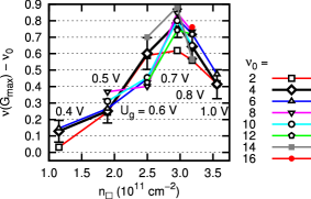
The expected magnetic shift of the anticrossings is small if one considers the energy scale not absolutely, but in units of the cyclotron energy. According to the band structure of Fig. 3b, the band gaps are shifted by . Likewise, the conductance traces of Fig. 5a have peaks with positions which depend on the magnetic field. The peaks are shifted for an increasing electron density towards higher filling factors. For , they move to lower values again. In the following, a basis filling factor , 4, 6, is assigned to the particular peaks of each conductance trace. The difference between the actual peak position and is plotted in Fig. 1. For a constant basis filling factor , the magnetic field increases in this graph from the left to the right. In order to keep the Fermi level within the same band gap, it is necessary to increase the electron density for compensating an enhanced degeneracy factor . The graphical comparison in Fig. 1 shows that the conductance peaks evolve in a very similar way for different basis filling factors.
The magnetic shift of the conductance peaks is compensated by another effect which emerges for gate voltages greater than 0.7 V. The corresponding decrease of the peak positions is not correlated with the magnetic field, but is a consequence of the internal bias voltage which builds up due to the gate leakage current. The potential offset between both electron films involves a lowering of the band gaps with respect to the electron system next to the cathode [12]. This effect shifts the conductance peaks towards lower filling factors and has been revealed in Ref. [8] by applying an external bias voltage. Our sample structure exhibits a very similar behavior for the internal bias. The pronounced boundary between rising and falling peak positions at is a consequence of the nearly exponential relation between the gate and bias voltages (Fig. 5c). Because the charge carrier density of both electron systems changes simultaneously with , the spectroscopy of a certain band gap for different internal bias voltages requires an adjustment of the magnetic field. Hence, the displacement of the conductance peaks cannot be investigated independently from the magnetic shift of the Landau gaps. Nevertheless, a quantitative comparison with the results of Kang et al., who applied an external bias, reveals similar peak shifts. For a gate voltage which increases from 0.7 to 1.0 V, the position of the peak diminishes in Fig. 1 by . At the same time, the internal bias rises according to Fig. 5b by . For this voltage offset, the first conductance peak in Fig. 2 of Ref. [8] decreases from to 1.04. Thus, the shift obtained for an external bias is comparable to the displacement encountered for an internal bias of the same amplitude.
| 0.4 | 1.16 | 1.15 | 4.13 | 2.062 | 2.072 |
|---|---|---|---|---|---|
| 0.5 | 1.89 | 1.84 | 4.24 | 2.078 | 2.091 |
| 0.6 | 2.49 | 2.25 | 4.58 | 2.086 | 2.100 |
| 0.7 | 2.95 | 2.56 | 4.77 | 2.092 | 2.107 |
| 0.8 | 3.18 | 2.84 | 4.63 | 2.097 | 2.113 |
All conductance peaks in Fig. 1 are shifted towards higher filling factors as the gate voltage increases up to 0.7 V. Due to the cropping of the conductance peak at (this feature will be discussed in Sec. 7), the following quantitative analysis is focused on the peak which can be localized much more accurately. The band gap which is responsible for this conductance peak is twofold, more precisely, it consists of two anticrossings at opposed wave numbers (Fig. 3). Table 1 compares the positions of the conductance peak for different magnetic fields with the result of corresponding band structure calculations. The relevant band gap is characterized either by its extension or its center and width . For an increase of the gate voltage from 0.4 to 0.5 V, the magnetic field is raised from 1.15 to 1.84 T in order to compensate for the enhanced electron density and to keep the Fermi level between the Landau bands and . This shift corresponds to a displacement of the conductance peak by on the scale of the filling factor. According to the band structure calculation, the higher magnetic field raises the energy gap by . The conversion to the filling factor doubles this value: . For another data set, which is not shown here, we get and , respectively.
The ratio between the measured and predicted shift of the conductance peak is . The discrepancy between both values is not yet completely resolved, but it is probably a consequence of the Coulomb interaction which is not considered in the calculated Landau dispersion. The influence of this many body effect on the band gap size is investigated in Refs. [26] and [27]. Both author groups arrive at the result that the electron-electron interaction enhances the energy gaps by a factor of about two. The absolute position of the band gaps is, however, not explicitly determined there. Generally, the opposite edge channels are converging with an increasing magnetic field according to , with the consequence that the total Coulomb energy rises. This effect is most likely responsible for the encountered enhancement of the conductance peak displacement.
7. Aharonov-Bohm effect
The Landau dispersion as discussed so far is valid for a perfect tunneling barrier which is invariant in the -direction. Within a real barrier, however, there exist imperfections which lead to a local enhancement of the tunneling probability. These tunneling centers, which are considered in the model of Kim and Fradkin [9], give rise to Aharonov-Bohm (AB) interferences between the opposite edge channels along the barrier [10, 11]. In addition, the point contacts are responsible for conductance fluctuations observed at low magnetic fields [12]. The latter effect which appears before the formation of distinct quantum Hall edge channels will be discussed in Sec. 8.
The rightmost resistance minimum of the curves in Fig. 2b shows some irregularities which are most pronounced for and disappear at higher gate voltages. Figure 7a gives a magnification of this feature. The left conductance peak is substantially cropped and the peak at also exhibits slight irregularities. In general, there exist two different types of oscillations which appear simultaneously and exclusively at the first conductance peak on the scale of the filling factor: short-period and quasiperiodic AB oscillations as well as long-period conductance fluctuations. A visual differentiation between both effects is possible by the black curves in Figs. 7a and b. The two measurements differ only with respect to the sweep velocity of the magnetic field. A high value for in the right plot averages the AB oscillations out, whereas in Fig. 7a both oscillation types are visible. The two kinds of conductance fluctuations are not simply superimposed to the long-range Landau oscillations, but they come along with a cropping and flattening of the respective conductance peak. While Fig. 7 reveals a clear distortion of the conductance peak at 400 mK, the same maximum is in Fig. 1(a) of Ref. [22] for 300 mK entirely smooth. However, in Ref. [10] also a sample of Kang et al. shows a strong cropping of the conductance peak at a slightly lower temperature of 220 mK.
[t]
![[Uncaptioned image]](/html/0709.3625/assets/x9.png) \vchcaptiona)
Conductance traces for different gate voltages. b) Variation of the
tunneling current at constant and
. The measurements have been carried out at an
increased field sweep velocity.
\vchcaptiona)
Conductance traces for different gate voltages. b) Variation of the
tunneling current at constant and
. The measurements have been carried out at an
increased field sweep velocity.
The phase coherence of the interfering electrons is harmed by both thermal fluctuations and electrostatic potential gradients. The critical temperature given by Eq. (9) separates the coherent and incoherent regime. The calculation of the band structure for the mean magnetic field 3.5 T of the first conductance peak yields for the two involved opposite edge channels (inset of Fig. 7b). In anticipation of the mean distance of the tunneling centers, , the critical temperature is then . This result is insofar plausible as the AB oscillations of Fig. 7a are almost suppressed at 370 mK () while in Ref. [10] they exhibit at 25 mK an amplitude which is more easily recognizable ().
Each phase-destroying effect which appears in addition to thermal fluctuations causes that some tunneling paths, first of all those with point contacts at a great distance, lose their coherence. Thereby, the shape of the conductance fluctuations changes since they are composed of all coherent AB oscillations. The quantum interferences are influenced by the internal voltage in a similar way as by thermal fluctuations. Due to the potential gradient across the barrier, a tunneling electron possesses an excess energy with respect to the Fermi level of the destination system. The bigger this difference, the more free states are available around the final wave number, and the more electron-electron scattering processes cause a loss of the phase information [28]. Analogous to the thermal disorder, this effect is negligible as long as
| (15) |
holds. The energy equivalent to the critical temperature is . Consequently, the AB oscillations are expected to be essentially undisturbed until the internal bias voltage exceeds 11 V. This threshold is reached in Fig. 5b for a gate voltage of 0.498 V. Indeed, the conductance trace for shows in Fig. 7a a significant indication of an initially emerging incoherence: In comparison to the data for , the right part of the conductance peak is already partially smoothed for . The effect is further intensified at in that the cropping of the peak almost disappears while the AB signatures persist only at the curve shoulder around . Thus, the bias coherence condition is essentially consistent with the experimental data as well as this is the case for the temperature dependence.
![[Uncaptioned image]](/html/0709.3625/assets/x10.png) \vchcaption
\vchcaption
a) Magnification of the cropped conductance peak at . The derivative is shown for two different field sweeps where the curve for 480 mK is shifted downward for clarity. b) Fast Fourier transform of for a field range of 2.93–4.26 T. Inset: the Landau dispersion (blue) and two wave functions are plotted vs and , respectively. The shown energy eigenstates with lie slightly below the first anticrossing at 1.09. The arrows located at a distance of indicate the center of mass of the left (red) and right (green) edge channel.
Although the amplitude of the AB oscillations shown in Fig. 7a is rather small, they are clearly revealed in the derivative of . This is possible even for a high temperature of about 500 mK which substantially exceeds the critical temperature of . The conductance traces, which are composed of data points at a distance of 1.4 mT, are smoothed before the differential quotient is calculated. For this purpose, parabolas are fitted to the curve for each data point by considering altogether 12 points in the proximity of the central point. The slope of the parabola at the abscissa of the middle sampling point is plotted in Fig. 7a. The comparison of two successive field sweeps reveals that all fine structures of the conductance traces are reproducible to a very high degree. It is possible to resolve half cycles with a minimum width of 5 mT and an amplitude of at least . The derivative exhibits a strong quasiperiodic character which gives evidence that there exist more than two tunneling centers within the barrier. More precisely, this is an indication that several pairs of point contacts simultaneously fulfill the coherence conditions of Eqs. (10) and (15). The Fourier spectrum of Fig. 7b is mainly concentrated within the two period length intervals 52–79 mT and 106–144 mT. The comparison of the spectrum with the conductance trace in Fig. 7a suggests that the components of the second interval represent the second harmonic of the long-period conductance fluctuations. The latter have a period of if the quantity is determined directly from . The origin of these fluctuations will be discussed below.
According to Eq. (7), the distance of two tunneling centers which cause AB oscillations of a period is . The distance of the involved edge channels can be determined either by the approximation formula of Eq. (8) or from a dedicated band structure calculation. The wave functions shown in the inset of Fig. 7b are located with their energy level next to the first band gap and have a distance of if the expectation value for the -location is considered. For comparison, Eq. (8) yields for the two states with an approximated distance of . Because the Landau dispersion varies only slightly on the scales of the magnetic length and the cyclotron energy, the exact result is also a good approximation for system parameters which differ from those of Fig. 7. However, in units of the barrier width, the quantity may vary considerably: In our case (, ), the distance of the edge channels is while for the conditions of Ref. [10] one gets . Generally, the distance of the opposite edge channels at a thin barrier is less determined by the barrier width, but rather by the extension of the wave functions.
The first interval of the Fourier spectrum of Fig. 7b contains contributions of prominent AB oscillations with periods of , 63, and 74 mT. If the distance between the interfering edge channels is , these values correspond to a distance of the tunneling centers of , 2.0, and 1.7 m, respectively. However, as the resolution of the Fourier spectrum is limited to about 4 mT due to the finite width of the conductance peak, reliable conclusions about the actual configuration of the tunneling centers are not reasonable, so that we simply state the average distance of the point contacts: . If a pair of tunneling centers with a distance of belongs to the coherent regime according to Eq. (10), the phase coherence length is at least which follows from Fig. 4c. Thus, our experimental data yields .
The AB oscillations are superimposed by slowly varying conductance fluctuations which have according to Fig. 7b a period length of about 0.23 T. The authors of Ref. [10] report a similar period of about 0.2 T. The long-period conductance fluctuations occur in our samples for temperatures up to . Since this feature simultaneously emerges with the AB oscillations and disappears together with them when the internal bias increases (Fig. 7a), a connection to the quantum interferences at tunneling centers is obvious. However, the theoretical work of Ref. [9] gives no direct evidence for this effect. Nevertheless, from microstructured AB rings it is well-known that AB oscillations, which are periodic with respect to the flux quantum , simultaneously arise along with aperiodic fluctuations which have a higher amplitude as well as a considerably longer period [21, 29]. The effect is attributed to the finite width of an AB ring [30]. When the electrons diffuse through the mesoscopic system, the corresponding trajectories lie from time to time nearer to the inner or outer radius of the ring-shaped electron path. The corresponding fluctuations of the enclosed magnetic flux exist in addition to the continuous variation due to a rising or falling magnetic field. The random shape of the electron trajectories within the conductor determines the phase difference between both pathways and is reflected by irregular fluctuations of the conductance. The effect can be reduced or avoided if the area of the AB ring is very small compared to the area circumscribed by the whole ring path [30].
In contrast to conventional AB rings, the interfering electrons in our sample are not kept enclosed by a conductance path. Their location is rather determined by the magnetic confinement potential in combination with the shape of the conductance band. For a varying magnetic field, the enclosed flux changes by reason of two different effects: Besides the proportionality with respect to the magnetic field, the latter also controls the flux indirectly via the distance of the interfering edge channels. The field-dependence of this length comes from the Landau dispersion and can be described according to Eq. (8) by the relation . The parameter is a smooth function of the magnetic field only for an ideal system. In a real sample, the field-induced variation of the channel positions is additionally influenced by the disorder potential. The spatial shift of the edge channels is irregularly modified when the electrons at the Fermi edge are forced by the disorder potential to propagate along a trajectory which deviates from that expected for a perfect rectangular potential wall. Because of and , it is possible that small displacements of the edge channels cause a variation of the enclosed magnetic flux on the order of the flux quantum. However, due to the local character of disorder, the effect emerges in comparison to AB oscillations on considerably larger scales of the magnetic field. The corresponding long-period and irregular conductance oscillations represent an abstract image of the disorder at the tunneling barrier.
8. Conductance fluctuations at low magnetic fields
The AB effect is restricted to the conductance peak which corresponds to the lowest Landau band gap. Already at the subsequent peak, the irregular oscillations are almost completely suppressed (Fig. 7). Though the AB signatures rapidly disappear from the conductance traces for a decreasing magnetic field, similar fluctuations emerge at low field strengths again (Fig. 8a). The quasiperiodic oscillations start from zero field, get considerably stronger at about 0.27 T and vanish at 0.8 T when the regular Landau oscillations arise. Just like the AB oscillations, the conductance feature in the low field regime is characterized by a quasiperiodic behavior and a high reproducibility. Furthermore, the Fourier spectrum (inset of Fig 8a) extends over a similar range of period, namely, –65 mT.
[t]
![[Uncaptioned image]](/html/0709.3625/assets/x11.png) \vchcaptiona)
Highly reproducible conductance fluctuations at small magnetic
fields. The lower graph is shifted by for
clarity. The inset contains the Fourier analysis of for
. b) Conductance traces for different gate
voltages. For pointing out the details, each curve is plotted as the
twentyfold difference between and a straight line which is
fitted to the experimental data. The circles mark the critical
field at which quasiperiodic oscillations with an amplitude of
become visible.
\vchcaptiona)
Highly reproducible conductance fluctuations at small magnetic
fields. The lower graph is shifted by for
clarity. The inset contains the Fourier analysis of for
. b) Conductance traces for different gate
voltages. For pointing out the details, each curve is plotted as the
twentyfold difference between and a straight line which is
fitted to the experimental data. The circles mark the critical
field at which quasiperiodic oscillations with an amplitude of
become visible.
In spite of the resemblance between the conductance fluctuations at low magnetic fields and the quasiperiodic AB oscillations, there is evidence that the low field feature is not based upon the interference between counterpropagating edge channels. The conductance traces of Fig. 8b exhibit fluctuations which do not disappear for an increasing gate voltage as it is the case for the AB oscillations in Fig. 7a. This indicates that the quantum interferences do not take place immediately within the internal bias gradient, but they emerge apart from the tunneling barrier. Granted that the conductance feature at low magnetic fields was caused by the quantum interference of counterpropagating edge channels, one would expect according to Eqs. (7) and (8) a period length of
| (16) |
In contrast to the AB oscillations at the peak, the field-dependence of the period length cannot be neglected in the low field regime. Though the conductance traces of Fig. 8b fulfill at some degree, the absolute period of the conductance fluctuations does not conform to the theoretical prediction of Eq. (16): For the average distance of the tunneling centers and the field range 0.27–0.80 T this formula yields a period of 8–23 mT which substantially deviates from the Fourier spectrum of the experimental data.
The conductance fluctuations at low magnetic fields originate most likely from the bulk of the 2DESs. Recently, it has been shown with a cooled scanning probe microscope that electrons which are injected through a quantum point contact into a 2DES flow at zero magnetic field along fan-shaped branches [31, 32]. If just one transversal mode passes the contact, the electrons are restricted to a single branch. In our sample, the AlGaAs barrier contains tunneling centers which are randomly distributed over the long potential wall. From their average distance of 2 m, one may estimate the number of tunneling centers to be on the order of one hundred. In comparison, the 2DESs with the electron density of at possess transversal modes [28]. Even if the momentum relaxation length fell below the phase coherence length by two orders of magnitude, the localization length still clearly exceeds the extension of the electron systems in the -direction. In addition, the short electron systems represent a single phase coherence unit, , and, therefore, belong to the regime of weak localization. However, this effect does generally not cause conductance fluctuations in broad samples and would be anyway destroyed by low magnetic fields [28]. As the imperfect potential barrier reduces the mode number of the total system by at least two orders of magnitude, strong localization () becomes possible. In this regime, the electron branches which stem from the multiple slits in the tunneling barrier interfere and cause conductance fluctuations while the Fermi level or the magnetic field are varied. This effect vanishes at about 0.8 T when all electrons which are injected by the tunneling centers are forced by the magnetic field to propagate within the same edge channels, cf. Ref. [32], so that the fluctuating electron branches in the bulk of the electron systems do not exist any longer.
The conductance fluctuations in the low field regime allow—similar to the AB oscillations—an estimation of the phase coherence length. The starting point is the semiclassical condition which requires electrons to fulfill at least one complete cyclotron orbit. The critical magnetic field is determined by the onset of significant oscillations which are defined here ad hoc as a ‘dense sequence’ of fluctuations with an amplitude of minimally . For the conductance curve with in Fig. 8b, this definition yields a phase coherence mobility of . This quantity corresponds to a phase coherence length of which is of the same order as the value obtained from the AB oscillations. For an increasing gate voltage, the momentum relaxation time rises due to a more efficient screening of remote ionized scatterers. The corresponding increase of the phase coherence length [28] is, indeed, confirmed by a decrease of in Fig. 8b.
9. Summary
We have presented a GaAs/AlGaAs heterostructure which contains two laterally adjacent, field-induced quantum Hall systems which are separated by a thin, epitaxially grown barrier. The structure includes a gate electrode in order to allow a detailed analysis of the Landau band structure at the line junction for different magnetic fields. For the interpretation of the experimental data, the Landau dispersion has been calculated exactly for non-interacting electrons residing in a 2DES with a rectangular potential wall. The conductance traces in dependence of the magnetic field are dominated by so-called Landau oscillations which occur due to the periodic coincidence of the Fermi level with the Landau band gaps. An observed enhancement of the conductance which exceeds the predictions according to the Landauer-Büttiker formalism is a consequence of macroscopic defects. The latter divide the long and narrow quantum region into multiple independent sections which are connected in parallel by the extended -contact layers. Our theory predicts for weakly coupled electron systems a magnetic shift of the anticrossings on the scale of the cyclotron energy of about 1/50 T. The experiment confirms this effect semiquantitatively by a displacement of the conductance peaks on the scale of the filling factor for an increasing Fermi level.
The conductance peak which corresponds to the gap between the first two Landau bands is cropped and distorted by short- and long-period conductance fluctuations. The short-period feature is a result of the AB interference between counterpropagating edge channels along the barrier. The interference is made possible by tunneling centers which exist accidentally within the AlGaAs barrier. For determining the distance of the involved tunneling centers from the Fourier spectrum of the conductance traces, it is necessary to know the distance of the interfering edge channels. By using the result of a band structure calculation, we obtain an average distance of the point contacts of about 2 m. The observed AB oscillations basically fulfill two coherence conditions which describe the influence of the electron temperature and the internal bias voltage, respectively. The bias results from gate leakage currents which lead to an offset between the two coupled electron systems. Long-period conductance fluctuations at the first conductance peak are a consequence of the disorder potential which distorts the edge channel positions in an irregular way for a varying magnetic field.
In addition to the interference effects at the cropped conductance peak, we observe conductance fluctuations which emerge at small magnetic fields and disappear at the onset of the regular Landau oscillations. They occur in the regime of strong localization which is a consequence of an imperfect barrier. The latter represents a multiple slit interferometer which essentially reduces the number of transversal modes in the whole system. The phase coherence length determined from the conductance fluctuations, , is of the same order as which follows from the distance of the tunneling centers involved for the AB oscillations.
This work was supported financially by the Deutsche Forschungsgemeinschaft (DFG) via the priority program Quanten-Hall-Systeme. We would like to thank M. Bichler and G. Abstreiter as well as M. Reinwald for sample growths. M. H. is grateful to M. Grayson for useful and motivating discussions throughout this project.
References
- [1] L. D. Landau, Z. Phys. 64, 629 (1930).
- [2] B. I. Halperin, Phys. Rev. B 25, 2185 (1982).
- [3] A. H. MacDonald and P. Středa, Phys. Rev. B 29, 1616 (1984).
- [4] K. v. Klitzing, G. Dorda, and M. Pepper, Phys. Rev. Lett. 45, 494 (1980).
- [5] L. Pfeiffer, K. W. West, H. L. Stormer, J. P. Eisenstein, K. W. Baldwin, D. Gershoni, and J. Spector, Appl. Phys. Lett. 56, 1697 (1990).
-
[6]
M. Grayson, M. Huber, M. Rother, W. Biberacher,
W. Wegscheider, M. Bichler, and G. Abstreiter, Physica E 25, 212 (2004).
M. Huber, M. Grayson, M. Rother, W. Biberacher, W. Wegscheider, and G. Abstreiter, Phys. Rev. Lett. 94, 016805 (2005). - [7] T.-L. Ho, Phys. Rev. B 50, 4524 (1994).
- [8] W. Kang, H. L. Stormer, L. N. Pfeiffer, K. W. Baldwin, and K. W. West, Nature (Lond.) 403, 59 (2000).
- [9] E.-A. Kim and E. Fradkin, Phys. Rev. B 67, 045317 (2003); Phys. Rev. Lett. 91, 156801 (2003).
- [10] I. Yang, W. Kang, L. N. Pfeiffer, K. W. Baldwin, K. W. West, E.-A. Kim, and E. Fradkin, Phys. Rev. B 71, 113312 (2005).
- [11] M. Habl, M. Reinwald, W. Wegscheider, M. Bichler, and G. Abstreiter, Phys. Rev. B 73, 205305 (2006).
- [12] M. Habl, Ph.D. thesis, Universität Regensbug (2006).
- [13] Y. Takagaki and K. H. Ploog, Phys. Rev. B 62, 3766 (2000).
- [14] The complete algorithm, including the consideration of the effect of different effective masses in GaAs and AlGaAs, is to be published separately.
- [15] R. Schuster, H. Hajak, M. Reinwald, W. Wegscheider, G. Schedelbeck, S. Sedlmaier, M. Stopa, S. Birner, P. Vogl, J. Bauer, D. Schuh, M. Bichler, and G. Abstreiter, phys. stat. sol. (c) 1, 2028 (2004).
-
[16]
T. Feil, C. Gerl, and W. Wegscheider, Phys. Rev. B 73,
125301 (2006).
T. Herrle, Ph.D. thesis, Universität Regensburg (2007). - [17] I. Bartoš and B. Rosenstein, J. Phys. A: Math. Gen. 27, L53 (1994); phys. stat. sol. (b) 193, 411 (1996).
- [18] S. Adachi, GaAs and related materials (World Scientific, Singapore, 1994).
-
[19]
A. Erdélyi (ed.), Higher Transcendental Functions (McGraw-Hill,
New York, 1953).
J. Spanier and K. B. Oldham, An Atlas of Functions (Springer, Berlin, 1987).
W. Magnus, F. Oberhettinger, and R. P. Soni, Formulas and Theorems for the Special Functions of Mathematical Physics (Springer, Berlin, 1966). - [20] L. D. Landau and E. M. Lifshitz, Quantum mechanics (Pergamon, Oxford, 1965).
-
[21]
R. A. Webb, S. Washburn, C. P. Umbach, and R. B. Laibowitz,
Phys. Rev. Lett. 54, 2696 (1985).
R. Webb and S. Washburn, Phys. Today 41 (12), 46 (1988). - [22] I. Yang, W. Kang, K. W. Baldwin, L. N. Pfeiffer, and K. W. West, Phys. Rev. Lett. 92, 056802 (2004).
- [23] C. Weisbuch and C. Hermann, Phys. Rev. B 15, 816 (1977).
- [24] J. Dempsey, B. Y. Gelfand, and B. I. Halperin, Phys. Rev. Lett. 70, 3639 (1993).
-
[25]
A. Usher, R. J. Nicholas, J. J. Harris, and
C. T. Foxon, Phys. Rev. B
41, 1129 (1990).
V. T. Dolgopolov, A. A. Shashkin, A. V. Aristov, D. Schmerek, W. Hansen, J. P. Kotthaus, and M. Holland, Phys. Rev. Lett. 79, 729 (1997).
T.-Y. Huang, Y.-M. Cheng, C.-T. Liang, G.-H. Kim, and J. Y. Leem, Physica E 12, 424 (2002). - [26] A. Mitra and S. M. Girvin, Phys. Rev. B 64, 041309 (2001).
- [27] M. Kollar and S. Sachdev, Phys. Rev. B 65, 121304 (2002).
- [28] S. Datta, Electronic transport in mesoscopic systems (Cambridge University Press, 1997).
- [29] C. P. Umbach, S. Washburn, R. B. Laibowitz, and R. A. Webb, Phys. Rev. B 30, 4048 (1984).
- [30] A. D. Stone, Phys. Rev. Lett. 54, 2692 (1985).
- [31] M. A. Topinka, B. J. LeRoy, S. E. J. Shaw, E. J. Heller, R. M. Westervelt, K. D. Maranowski, and A. C. Gossard, Science 289, 2323 (2000).
- [32] K. E. Aidala, R. E. Parrott, T. Kramer, E. J. Heller, R. M. Westervelt, M. P. Hanson, and A. C. Gossard, Nat. Phys. 3, 464 (2007).