Demonstration of optically modulated dispersion forces
F. Chen,1 G. L. Klimchitskaya,2 V. M. Mostepanenko,3 and U. Mohideen1
1Department of Physics, University of California, Riverside, California 92521, USA.
2North-West Technical University, St.Petersburg, 191065, Russia.
3Noncommercial Partnership “Scientific Instruments”, Moscow, 103905, Russia.
Umar.Mohideen@ucr.edu
Abstract
We report the first experiment on the optical modulation of dispersion forces through a change of the carrier density in a Si membrane. For this purpose a high-vacuum based atomic force microscope and excitation light pulses from an Ar laser are used. The experimental results are compared with two theoretical models. The modulation of the dispersion force will find applications in optomechanical micromachines.
OCIS codes: (270.0270) Quantum optics
References and links
- [1] J. Mahanty and B. W. Ninham, Dispersion Forces (Academic Press, New York, 1976).
- [2] P. W. Milonni, The Quantum Vacuum (Academic Press, Boston, 1994).
- [3] M. Kardar and R. Golestanian, “The “friction” of vacuum and other fluctuation-induced forces,” Rev. Mod. Phys. 71, 1233–1245 (1999).
- [4] V. A. Parsegian, Van der Waals Forces: A Handbook for Biologists, Chemists, Engineers, and Physicists (Cambridge University Press, Cambridge, 2005).
- [5] E. V. Blagov, G. L. Klimchitskaya, and V. M. Mostepanenko, “Van der Waals interaction between microparticle and uniaxial crystal with application to hydrogen atoms and multiwall carbon nanotubes,” Phys. Rev. B 71, 235401-1–12 (2005).
- [6] H. Oberst, Y. Tashiro, K. Shimizu, and F. Shimizu, “Quantum reflection of He∗ on silicon,” Phys. Rev. A 71, 052901-1–8 (2005).
- [7] B. S. Stipe, M. J. Mamin, T. D. Stowe, T. W. Kenny, and D. Rugar, “Noncontact friction and force fluctuations between closely spaced bodies,” Phys. Rev. Lett. 87, 096801-1–4 (2001).
- [8] E. Buks and M. L. Roukes, “Stiction, adhesion energy, and the Casimir effect in micromechanical systems,” Phys. Rev. B 63, 033402-1–4 (2001).
- [9] R. S. Decca, E. Fischbach, G. L. Klimchitskaya, D. López, D. E. Krause, and V. M. Mostepanenko, “Improved test of extra-dimensional physics and thermal quantum field theory from new Casimir force measurements,” Phys. Rev. D 68, 116003-1–15 (2003).
- [10] R. S. Decca, D. López, E. Fischbach, G. L. Klimchitskaya, D. E. Krause, and V. M. Mostepanenko, “Precise comparison of theory and new experiment for the Casimir force leads to stronger constraints on thermal quantum effects and long-range interactions,” Ann. Phys. 318, 37–80 (2005).
- [11] R. S. Decca, D. López, E. Fischbach, G. L. Klimchitskaya, D. E. Krause, and V. M. Mostepanenko, “Tests of new physics from precise measurements of the Casimir pressure between two gold-coated plates,” arXiv: hep-ph/0703290; to appear in Phys. Rev. D.
- [12] M. Bordag, U. Mohideen, and V. M. Mostepanenko, “New developments in the Casimir effect,” Phys. Rep. 303, 1–205 (2001).
- [13] E. M. Lifshitz and L. P. Pitaevskii, Statistical Physics. II (Pergamon, Oxford, 1980).
- [14] B. Geyer, G. L. Klimchitskaya, and V. M. Mostepanenko, “Thermal quantum field theory and the Casimir interaction between dielectrics,” Phys. Rev. D 72, 085009-1–20 (2005).
- [15] F. Chen, U. Mohideen, G. L. Klimchitskaya, and V. M. Mostepanenko, “Investigation of the Casimir force between metal and semiconductor test bodies,” Phys. Rev. A 72, 020101(R)-1–4 (2005).
- [16] F. Chen, U. Mohideen, G. L. Klimchitskaya, and V. M. Mostepanenko, “Experimental test for the conductivity properties from the Casimir force between metal and semiconductor,” Phys. Rev. A 74, 022103-1–14 (2006).
- [17] F. Chen, G. L. Klimchitskaya, V. M. Mostepanenko, and U. Mohideen, “Demonstration of the difference in the Casimir force for samples with different charge-carrier densities,” Phys. Rev. Lett. 97, 170402-1–4 (2006).
- [18] S. G. Rabinovich, Measurement Errors and Uncertainties (Springer, New York, 2000).
- [19] W. Arnold, S. Hunklinger, and K. Dransfeld, “Influence of optical absorption on the van der Waals interaction between solids,” Phys. Rev. B 19, 6049–6056 (1979).
- [20] E. D. Palik (ed.), Handbook of Optical Constants of Solids (Academic, New York, 1985).
- [21] T. Vogel, G. Dodel, E. Holzhauer, H. Salzmann, and A. Theurer, “High-speed switching of far-infrared radiation by photoionization in a semiconductor,” Appl. Opt. 31, 329–337 (1992).
- [22] E. Yablonovitch, D. L. Allara, C. C. Chang, T. Gmitter, and T. B. Bright, “Unusually low surface-recombination velocity on silicon and germanium surfaces,” Phys. Rev. Lett. 57, 249–252 (1986).
- [23] A. A. Maradudin and P. Mazur, “Effects of surface roughness on the van der Waals force between macroscopic bodies,” Phys. Rev. B 22, 1677–1686 (1980).
- [24] J. M. Obrecht, R. J. Wild, M. Antezza, L. P. Pitaevskii, S. Stringari, and E. A. Cornell, “Measurement of the temperature dependence in the Casimir-Polder force,” Phys. Rev. Lett. 98, 063201-1–4 (2007).
1 Introduction
Dispersion forces [1], which is a generic name for van der Waals and Casimir forces [2], are of vital importance in diverse systems and phenomena, such as membranes and layered structures [3], chemical and biological processes [4], carbon nanotubes [5], Bose-Einstein condensation [6], noncontact atomic friction [7], nanoelectromechanical devices [8] and as a test for predictions of modern unification theories [9–11]. Modern measurements of dispersion forces are reviewed in [12]. The basic theory of dispersion forces was developed by Lifshitz [13]. However, the application of this theory to real materials at nonzero temperature faces problems [14]. Here we first demonstrate the optical modulation of dispersion forces through a change in the carrier density by the absorption of photons. For this purpose a high-vacuum based atomic force microscope (AFM) is used to measure the modification in the force between a gold coated sphere and a single-crystalline Si membrane. The excitation of the carriers in Si is done with 514 nm light pulses from an Ar laser. Our experimental results are in agreement with the Lifshitz theory if, in the absence of excitation light, the model description of Si allows a finite static dielectric permittivity. At the same time, the model taking into account the dc conductivity of high-resistivity Si is excluded by our measurements. The provided experimental results are topical for numerous applications of dispersion forces ranging from biology, optomechanics, tribology, condensed matter, atomic physics, and to string theory.
2 Experimental setup and measurement results
Illumination with laser light is an effective method to increase the carrier density of a semiconductor up to values of order required to observe the modification of dispersion forces. Our experimental setup used for the optical modulation of the dispersion force is shown in Fig. 1. A gold coated polystyrene sphere with a diameter m is mounted on the tip of a 320m conductive AFM cantilever at a distance above a single-crystalline Si membrane in a vacuum chamber. The thickness of gold coating on the sphere was measured to be nm. An oil free vacuum with a pressure of around Torr is used. The membrane is mounted on top of a piezo capable of traveling a distance up to 6m between the test bodies. The complete movement of the piezo, , was calibrated using a fiber optic interferometer. To extend and contract the piezo, continuous triangular voltages with frequencies between 0.01–0.02 Hz are applied to it. (Given that the experiment is done at room temperature, applying of static voltages would lead to piezo creep and loss of position sensitivity.)
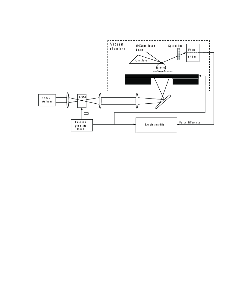
To modulate the dispersion force between the sphere and the membrane due to the excitation of carriers, we illuminate the membrane with 514 nm pulses, obtained from a CW Ar ion laser. The light is focused on the bottom surface of the membrane. The Gaussian width of the focused beam was measured to be mm. The cantilever flexes in response to the force changes. This deflection is monitored with an additional 640 nm laser beam reflected off the top of the cantilever tip and leads to a difference signal between two photodiodes (see Fig. 1). An optical filter was used to prevent the interference of the 514 nm excitation light with the cantilever deflection signal. The excitation laser light was modulated at a frequency of 100 Hz (5 ms wide light pulses) using an Acousto-Optic-Modulator (AOM). The AOM is triggered with a function generator. The same function generator is also used as a reference for the lockin amplifier, designed to measure the difference of dispersion forces in response to the carrier excitation, and for applying compensation voltages to the membrane (see below).
The illumination of the Si has to be done such that very little if any light impinges on the sphere, as this would lead to a light induced force from the photon pressure. As the Si membrane is illuminated from the bottom, care should be taken that the fraction of light transmitted through the membrane is negligibly small. Thus, the thickness of the membrane has to be greater than 1m which is the optical absorption depth of Si at a wavelength of 514 nm (rad/s). Calculations show that for our membrane of about m thickness the force on a sphere due to photon pressure varies from 2.7% to 8.7% of the difference of dispersion forces to be measured when separation changes from 100 to 200 nm. Fabrication of the Si device with a few micrometer thick single crystal membrane of orientation (colored black in Fig. 1 with white buried SiO2 layer) is necessary to accomplish the experimental conditions. It is achieved using a commercial Si grown on insulator wafer, subject to mechanical polishing, RCA cleaning and TMAH etching (details will be published elsewhere). An ohmic contact is formed by a thin film of Au deposited on the edge of Si device layer far away from its central part followed by annealing at 673 K for 10 min. The Si membrane surface was cleaned with Nanostrip and then passivated by dipping in 49% HF for 10 s. The passivated Si membrane was then mounted on top of the piezo as described above.
The calibration of the setup, determination of the cantilever deflection coefficient and the average separation on contact between the test bodies are performed as in earlier experiments with metal and semiconductor test bodies [12,15–17]. For the determination of the deflection coefficient, , and the separation on contact, , we apply different dc voltages between 0.65 to –0.91 V to the membrane at large separations from 1 to 5m, where the dispersion force is negligible. By fitting the experimental force-distance relation to the exact theoretical expression for the electrostatic force, where is the residual potential difference, is a known function [16], we arrive at nm per unit deflection signal and nm. Then the actual separations between the bottom of the gold sphere and the Si plate are given by . For the calibration of the deflection signal and the determination of the residual potential between the two surfaces, in addition to the dc voltages, a square voltage pulse of amplitude from 1.2 to –0.6 V is also applied to the membrane [16]. By fitting the difference signal to the exact theoretical expression, the calibration constant and the residual potential were obtained to be nN per unit cantilever deflection signal and V. All this was done in the same high vacuum setup.
Next the carriers were excited in the Si membrane by 514 nm laser pulses and the difference in the total force (electric and dispersion) with and without light
| (1) |
is measured by the lockin amplifier with an integration time constant of 100 ms which corresponds to a bandwidth of 0.78 Hz. Here is the difference in the dispersion force where is a force with (without) light. () is the still unknown residual potential difference between the sphere and the membrane during the bright (dark) phase of a laser pulse train (they may be different from the above-determined when no light is incident). () are voltages applied to the membrane during the bright (dark) phase of the laser pulse train. By keeping and changing , we measure the parabolic dependence of as a function of . The value of where the parabola reaches a maximum [recall that ] is . Then we keep , change and measure the parabolic dependence of on . The value of where this function reaches a minimum is . Both procedures were repeated at different separations and the values V and V were found to be independent of separation in the range from 100 to 500 nm reported below.
With these values of and , at every separation was determined from Eq.(1) using the measured value of . This was repeated with 41 pairs of different applied voltages () and the mean value of was found. Data were collected starting from contact at equal time intervals corresponding to 3 points per 1 nm. In Fig. 2 the experimental data for the mean as a function of separation varying from 100 to 500 nm (1209 points) are shown as dots. As is seen in Fig. 2, , i.e., the magnitude of the dispersion force with light is larger than without light in line with physical intuition (recall that we follow the definition of attractive forces as negative quantities). The variance of the mean , , decreases from 0.16 pN at nm to 0.11 pN at nm. Using Student’s -distribution with a number of degrees of freedom and choosing confidence, we obtain and . This leads to the variation of the random error of , equal to , from 0.34 pN at nm to 0.24 pN at nm. The systematic error in is determined from the resolution error in data acquisition, from the calibration error and from the total instrumental noise, and is equal to 0.09 pN at all separations. Thus, from statistical criterion [18], the total experimental error at 95% confidence is given by the random error. As a result, the relative experimental error changes from 10 to 25% when the separation increases from 100 to 180 nm. This allows us to conclude that the modulation of dispersion force with light is demonstrated at a high reliability and confidence. The observed effect cannot be due to the mechanical motion of the membrane. This is because vibrations due to heating (in our case less than 1∘C) would lead to different force-distance relationship in disagreement with our data in Fig. 2. Within the separation range from 180 to 250 nm the experimental error is less than 46%. At nm it reaches 100%. Note that there was an early attempt [19] to modify the dispersion force between a glass lens and a Si plate with light. However, glass is an insulator and therefore the electric forces such as due to work function potential differences could not be controlled. This might also explain that no force change occurred on illumination for small separations below 350 nm where it should be most pronounced.
3 Comparison with theory
For comparison of our experimental results with theory we have calculated the difference of dispersion forces from the Lifshitz formula. The calculations were done at the laboratory temperature K with the formula adapted for the configuration of a sphere above a plate [12] using the dielectric permittivities of gold and Si along the imaginary frequency axis. The at nonzero Matsubara frequencies , where is the Boltzmann constant, was found from the dispersion relation using the tabulated optical data for the complex refractive index [20]. As was shown in [10], the use of tabulated data leads to less than 0.5% error in the Casimir force [when the second body is a semiconductor, the calculational results are independent of what is substituted for ]. In the absence of excitation light, the dielectric permittivity of high-resisitivity Si, , was also found [14] from tabulated optical data (dashed line in Fig. 3). If we take into account the dc conductivity of high-resisitivity Si, the dielectric permittivity (dotted line in Fig. 3) is given by [15–17,20,21]
| (2) |
where and are the plasma frequency and the relaxation parameter for p-Si.

In the presence of light, the equilibrium value of the carrier density is rapidly established, during a period of time much shorter than the duration of the laser pulse. Therefore, we assume that there is an equilibrium concentration of pairs (electrons and holes) when the light is incident. The dielectric permittivity of Si in the presence of laser radiation is commonly represented by the Drude dielectric function which includes free charge carriers [15–17,20,21]
| (3) |
It is shown as the solid line in Fig. 3. Here the plasma frequencies and relaxation parameters for electrons and holes are introduced. The values of the relaxation parameters and effective masses are [21] rad/s, rad/s, , . From with a charge carrier concentration [20] for Si of high resistivity cm we obtain rad/s. In our experiment the uniform equilibrium concentration of charge carriers induced by the laser radiation in the region with a diameter equal to the Gaussian width of the beam is , where is the excited carrier lifetime and mW is the measured power absorbed for a surface area . The incident power is 13.7 mW. The lifetime ms was independently measured using a non-invasive optical pump-probe technique for the same membrane. The Ar laser beam modulated at 100 Hz to produce 5 ms wide square light pulses, as used in the Casimir force measurement, was employed as the pump. A CW beam with a 1 mW power at a wavelength of 1300 nm was used as the probe. The change in the reflected intensity of the probe beam in the presence and in the absence of Ar laser pulse was detected with a InGaAs photodiode. The reflected power of the probe beam was monitored as a function of time in an oscilloscope and found to be consistent with the change of carrier density. (The details will be reported elsewhere.) This results in a concentration of charge carriers induced by the incident light and, as a consequence, in rad/s, rad/s. A uniform carrier density in the membrane can be assumed, because of the long carrier diffusion lengths and the ability to obtain almost defect free surfaces in silicon through hydrogen passivation [22].
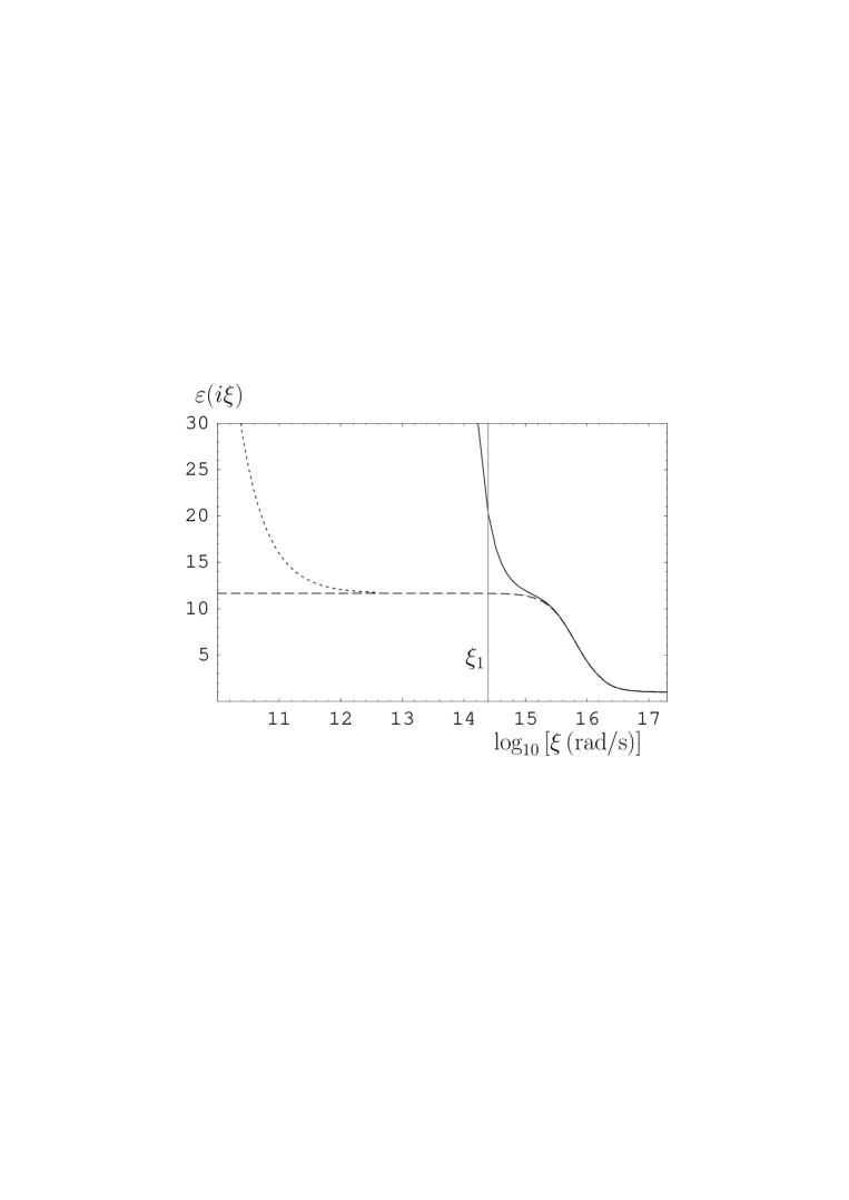
These values were used to calculate the theoretical force difference using the Lifshitz formula for two models of the dielectric permittivity of Si in the absence of laser light. The topography of both surfaces was investigated using an AFM and the effect of roughness [23] was taken into account as in [16]. It was found to be negligibly small. The solid line in Fig. 2 represents the difference force when in the absence of light the dielectric permittivity of Si is given by with the value . In this case the transverse electric coefficient for Si at zero Matsubara frequency is equal to zero as is true for any dielectric, , where is the momentum component in the plane of membrane. Thus, in the absense of laser light the obtained force does not depend on the value of the same coefficient for Au, , as only the product of both coefficients enters the Lifshitz formula (recall that there are different approaches in literature to the definition of ; see discussion in Refs. [9–11]). In the presence of light also holds true due to the functional form of the Drude model (3). In both cases at zero frequency only the transverse magnetic mode of the electromagnetic field contributes to the result. For dielectric Si in the absence of light . For Si in the presence of light and for Au holds. The solid line in Fig. 2 is in excellent agreement with data shown as dots. If the permittivity of Si in the absence of light is given by Eq. (2) (which includes dc conductivity at frequencies much below the first Matsubara frequency in Fig. 3), the force difference calculated from the Lifshitz formula is shown by the dashed line in Fig. 2 which disagrees with the experimental dotted line. In this case both in the absence and in the presence of light holds due to the properties of the Drude dielectric function. Once again, at zero frequency only the transverse magnetic mode contributes to the result. Here, however, for Si in the absence of light holds. Exactly this change in the magnitude of the transverse magnetic reflection coefficient at zero frequency leads to the deviation of the dashed line from the solid line in Fig. 2. It can be considered as somewhat surprising that the use of a more exact dielectric permittivity (2) instead of leads to the discrepancy between experiment and theory. This is, in fact, one more observation that there are puzzles concerning the applicability of the Lifshitz theory to real materials. In the case of metals, the Drude description of conduction electrons in the Casimir effect was excluded esperimentally in the series of experiments [9–11]. In the case of metals, the deviation of the experimental results from the Drude model approach is explained by the vanishing contribution from the transverse electric mode at zero frequency. The present experiment dealing with semiconductors is not sensitive enough to detect this effect. Here we report a novel effect due to the difference in the contributions of the zero-frequency transverse magnetic mode, which depends on whether or not the dc conductivity of Si in the absence of light is taken into account. Note that in [13] the dc conductivity of dielectrics is not taken into account. The same is true for the recent paper [24] on the thermal effects in the Casimir-Polder force. This suggests that the theory of dispersion forces between real materials requires further investigation.
The theoretical error in the computation of force difference varies from 13.6 to 16.0% when separation increases from 100 to 200 nm. Considering both the experimental and theoretical errors, the model of a high-resistivity Si using Eq.(2) is excluded by our experiment within the separation region from 100 to 200 nm at a 95% confidence.
4 Conclusion
In conclusion, we report the first experimental demonstration of the modulation of dispersion forces through optical modification of the carrier density of a Si membrane. Such modulation can be used in the design and function of optomechanical micromachines such as micromirrors, nanotweezers and nanoscale actuators.
Acknowledgments
The experimental section of the work was supported by the NSF Grant No. PHY0355092 and theory and analysis by DOE Grant No. DE-FG02-04ER46131.