Demonstration of the difference Casimir force for samples with different charge carrier densities
Abstract
A measurement of the Casimir force between a gold coated sphere and two Si plates of different carrier densities is performed using a high vacuum based atomic force microscope. The results are compared with the Lifshitz theory and good agreement is found. Our experiment demonstrates that by changing the carrier density of the semiconductor plate by several orders of magnitude it is possible to modify the Casimir interaction. This result may find applications in nanotechnology.
pacs:
12.20.Fv, 12.20.Ds, 68.37.Ps, 73.25.+iThe Casimir effect 1 implies that there is a force acting between closely spaced neutral bodies determined by the zero-point oscillations of the electromagnetic field. In the last few years the Casimir force was extensively investigated experimentally (see, e.g., Refs, 2 ; 3 ; 4 ; 5 ; 6 ; 7 ; 8 and review 9 ). It has found many diverse applications ranging from Bose-Einstein condensation 10 , carbon nanotubes 11 , and to the testing of predictions of new physics beyond the standard model 7 ; 8 ; 9 . One of the most important applications of the Casimir effect is in the design, fabrication and function of MEMS and NEMS such as micromirrors, nanotweezers and nanoscale actuators 13 ; 15 ; 16 . The combined action of the Casimir and electrostatic forces can result in nonlinear dynamics, bistable phenomena and even cause device failure by the abrupt “pull-in” and attachment of one surface to the other 13 ; 15 ; 16 . The Casimir force also changes the operation bandwidth and tunability of MEMS. The actuation of MEMS using the Casimir force has been demonstrated 16 .
The modification of the Casimir force by changing parameters of the system other than the separation is a complicated problem since it requires modification of the optical properties of materials within a relatively wide frequency region. The attempt to modify the Casimir force due to a coating with a hydrogen-switchable mirror did not lead to any observed effect 16a . We pioneer the demonstration of the difference Casimir force between a gold coated sphere and two Si samples which possess different resistivities and charge carrier densities. We use a high vacuum (Torr) based AFM to measure the Casimir force between a gold coated polystyrene sphere with a diameter m and two size Si plates placed next to each other. The thickness of gold coating on the sphere was measured to be nm. The details of the setup were described 17 in the previous experiment with one Si plate. For this experiment two identical polished, single crystal, orientation Si plates were chosen, 500 m thick and with a resistivity cm. They were -type and doped with P. The resistivity of the plates was measured using the 4-probe technique to be cm leading to the concentration of charge carriers . One of these samples was used as the first Si plate in the experiment. The other one was subjected to thermal diffusion doping to prepare the second, lower resistivity, plate. A phosphorous based Spin-On-Dopant (SOD) solution (P450 commercially available from Filmtronics Co.) was used. The wafers were spin-coated at a speed of rad/min for 0.25 min, followed by a pre-baking at 200 ∘C for 15 min on a hot plate. The sample was then placed in a diffusion furnace. The diffusion was carried out at 1000–1050 ∘C for 100 hours in a N2(75%)O2(25%) atmosphere. A 49% HF solution was used to etch off the residual dopant after the diffusion process. The effectiveness of the above procedure was determined using both a 4-probe resistivity measurement and a Hall measurement of a similarly doped 0.3 m thick single crystal Si grown epitaxially on Si wafer. This thin equivalent sample was homogenously doped under the above conditions 17a and allows a measurement of the carrier density. The resistivity and the carrier density were measured to be cm and . Both plates of higher and lower resistivity were subjected to a special passivation procedure to prepare their surfaces for the force measurements. For this purpose nanostrip (a combination of H2O2 and H2SO4) is used to clean the surface and 49% HF solution to etch SiO2 and to hydrogen terminate the surface 17 . Finally both plates were mounted in the AFM.
The calibration of the spring constant , measurements of the residual electrostatic potential , deflection coefficient and separation on contact were done using the experimental technique similar to what we have used in Refs. 4 ; 17 . All calibration and other measurements are done in the same high vacuum apparatus as the Casimir force measurements. The actual separation distance between the bottom of the gold sphere and Si plates is given by , where is the distance moved by the piezo and is the cantilever deflection signal from the photodiodes. First, the value of was found for the higher resistivity plate following the same procedure as in Ref. 17 . For this purpose the sphere was grounded and 29 different voltages between –0.712 to –0.008 V were applied to the plate through a thick gold pad attached to plate bottom. The change in the contact position between the sphere and the plate was used to find nm per unit deflection signal. Then the values of , (which in fact is needed for force measurements) and were found for the higher resistivity plate by fitting the deflection signal to the theoretical expression. From the definition of the deflection coefficient it follows . Here the electric force between a sphere and a plate is given by , where is the applied voltage and is a known function of separation (see Refs. 3 ; 4 ; 9 ; 17 for the explicit form of ). The voltage independent offset represents the contribution of the Casimir force to the signal and was found to match the value obtained in the independent measurement of the Casimir force. For the 29 different applied voltages the measured signal at every separation was plotted as a function of and fit to equation for . Note that the expression for the electric force used in the fit does not take into account possible influence of space-charge layer at the surface of high-resistivity Si. According to Ref. layer , for -type Si with the concentration of charge carriers of order the impact of this layer on the electrostatic force is negligible at separations larger than 300–400 nm. The use of the expression for electric force between metal surfaces may lead to nothing more than an increased error in the determination of . The fit was performed within the separation regions from 300–400 nm to 2.5 m. From the fit at every , the value V was obtained and verified to be independent of . The same fit results in the values of the cantilever calibration constant multiplied by the deflection coefficient pN per unit deflection signal, and the separation on contact nm.
After the calibration and related measurements for the higher resistivity sample are done, the Casimir force between this sample and the sphere was measured from contact as a function of distance. Here we report the results at nm to avoid the influence of nonlinearities associated with the “jump to contact” at shorter distances 17 . For this purpose the sphere was kept grounded while an appropriate compensating voltage was applied to the plate to cancel the residual electrostatic force. The distance between the sphere and the plate was changed continuously from large to short separations by applying triangular voltages at 0.02 Hz to the piezo. The force data were collected at equal time intervals corresponding to equidistant points separated by 0.17 nm. This measurement was repeated 40 times and the obtained forces were averaged to reduce the influence of different random factors including thermal noise, and particular positions on the silicon to which the sphere approaches. The mean values of the experimental Casimir force data as a function of separation are represented by dots labeled a in Fig. 1.
Next all the above calibrations and measurements were repeated for the second, lower resistivity, Si plate. In this case 25 different dc voltages between –0.611 to –0.008 V were applied to the plate. The deflection coefficient was equal to be nm per unit deflection signal. After the same fitting procedure of the measured deflection signal, the following values of all related parameters were obtained: V, nN per unit deflection signal, and nm. The fit was performed within the separation region from 100–300 nm to 2.5 m. Note that closer separations can be used as the effect of the space charge layer is negligible for the lower resistivity sample. The values of are slightly different in the two cases due to the changes in the cantilever level arm arising due to minor deviations from the horizontal position in the mounting of both samples. Next the Casimir force acting between the lower resistivity sample and the sphere was measured from contact after application of appropriate voltage to cancel the residual electrostatic force. We report the results in a linear regime at nm. This measurement was repeated 39 times. The resulting mean values of the Casimir force data as a function of are represented in Fig. 1 by dots labeled “b”. As is seen from the figure, dots labeled “a” and “b” are distinct from each other demonstrating the effect of different charge carrier densities in the two Si plates used.
For the quantitative characterization of the deviation between the two measurements, we calculate the random errors using the procedure outlined in Ref. 17 based on the Student’s distribution. For the sample of higher resistivity (measurement “a”) the random error at 95% confidence is equal to 8 pN at nm, decreases to 6 pN at nm and becomes equal to 4 pN at nm. The measurement “b” for the sample of lower resistivity is slightly more noisy. Here the random error at 95% confidence changes from 11 pN at nm, 7 pN at nm to 5 pN at nm. The systematic error at 95% confidence is equal to only 1.2 pN for both measurements (see Ref. 17 for details). Using the statistical criterion in Ref. 20 , we conclude that the total experimental errors determined at 95% confidence are equal to the random ones in each measurement. From Fig. 1 it is seen that the deviation between the two sets of data is larger than the total experimental error in the separation region from 61.19 to 120 nm.
Now we compare the force-distance relation measured for the two Si samples with the theory. At nm, where the differences between the two measurements are most pronounced, the magnitudes of the predicted thermal corrections are negligible 17 . At larger the relative contribution from thermal corrections is much less than the relative error of force measurements. Then the force between the sphere and one of the plates ( for higher and for lower resistivity Si) is given by the Lifshitz formula at zero temperature adapted for the configuration of a sphere above a plate 9 ; 22
| (1) |
The reflection coefficients for gold and for the two types of Si are expressed in the usual way 17 through the dielectric permittivities of gold and of Si along the imaginary frequency axis (). The permittivities and are computed by means of the dispersion relation using the tabulated optical data for the complex index of refraction 23 . The results are shown in Fig. 2 with the solid line and dashed line labeled “a”, respectively 24 . The permittivity of lower resistivity Si is found from 23 , where and are the plasma frequency and relaxation parameter of lower resistivity Si. Their values were found from rad/s and rad/s, where is the electron effective mass and is the permittivity of vacuum. The permittivity is shown in Fig. 2 by the dashed line labeled “b”. Then the forces and were calculated at all separations using Eq. (1).
The obtained results were corrected for the presence of surface roughness. To do this, the topographies of the sphere and both Si samples were investigated with an AFM. Then the scan data were used to additively compute the Casimir forces and starting from and and varying separations in accordance with the roughness profiles. The details of this procedure and justification of the additive approach for the experimental situation can be found in Refs. 4 ; 8 ; 17 . For both plates the contribution of the roughness to the Casimir force was equal. It changes from 3.6% of the total force at nm to 2.7, 1.4 and 0.65% at separations 70, 100 and 150 nm, respectively. Surface distortions on single crystal Si are very low and practically do not contribute to the roughness correction.
The errors in the computation of the Casimir force between the gold coated sphere and Si plate are analyzed in Ref. 17 . At the shortest they are mostly determined by the error nm (the plate “a”) and 0.8 nm (the plate “b”) in the measurement of separations with which the theoretical values of the Casimir force are calculated for the comparison with the experiment. A 0.5% error due to the variation of optical parameters 4 is also included. At nm the total theoretical error at 95% confidence is equal to 19.6 pN (4.9% of the force) for the plate “a” and to 17.2 pN (4.0% of the force) for the plate “b”. It decreases to 11 pN (4.2% of the force) for the plate “a” and to 9.6 pN (3.4% of the force) for the plate “b” at nm. The total theoretical error becomes less than the total experimental error at and 85 nm for the plates “a” and “b”, respectively.
The total theoretical error was combined with the total experimental error at 95% confidence using the statistical rule in Ref. 20 (see also Refs. 8 ; 17 ) to find the error of the difference between theoretical and experimental forces. The obtained confidence interval as a function of separation is shown in Fig. 3 as solid lines. The differences versus separation for the experiment with the higher resistivity Si are plotted in Fig. 3a as dots. Similarly, the differences for the lower resistivity Si are shown as dots in Fig. 3b. As is seen from Fig. 3, both measurements are consistent with theories using the dielectric permittivity (Fig. 3a) and (Fig. 3b).
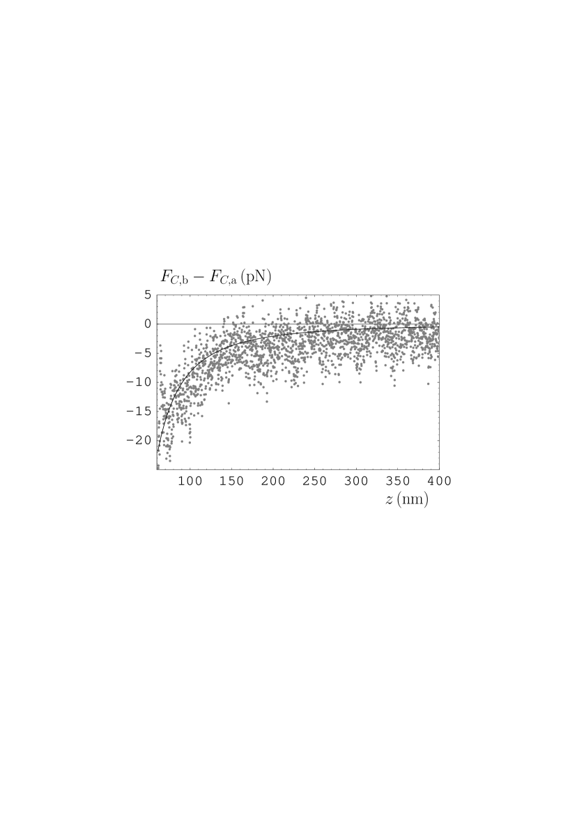
To illustrate the effect of modification of the Casimir force through the change of carrier density, in Fig. 4 we plot as dots the difference of the measured Casimir forces for the plates of lower and higher resistivities, , versus separation. In the same figure, the difference in the respective theoretically computed Casimir forces, is shown as the solid line. As is seen in Fig. 4, the experimental and theoretical difference Casimir forces as functions of are in good agreement. It can be easily shown that the magnitude of the mean difference of the measured Casimir forces exceeds the experimental error of force difference within the separations from 70 to 100 nm.
To conclude, we have measured the Casimir force between a gold coated sphere and two Si plates of higher and lower resistivity differing by several orders of magnitude. Each measurement was compared with theoretical results using the Lifshitz theory with different dielectric permittivities and found to be consistent with it. The difference of the measured forces for the two resistivities is in good agreement with the corresponding difference of the theoretical results. It takes a magnitude of about 17 pN at nm and decreases with increase of separation. The performed experiment demonstrates the possibility to modify the Casimir force by changing the carrier density of semiconductor materials which may find applications in the design, fabrication and function of MEMS and NEMS.
This work was supported by the NSF Grant PHY0355092 and DOE grant DE-FG02-04ER46131.
References
- (1) H. B. G. Casimir, Proc. K. Ned. Akad. Wet. 51, 793 (1948).
- (2) S. K. Lamoreaux, Phys. Rev. Lett. 78, 5 (1997).
- (3) U. Mohideen and A. Roy, Phys. Rev. Lett. 81, 4549 (1998); G. L. Klimchitskaya et al., Phys. Rev. A 60, 3487 (1999).
- (4) B. W. Harris, F. Chen, and U. Mohideen, Phys. Rev. A 62, 052109 (2000); F. Chen et al., Phys. Rev. A 69, 022117 (2004).
- (5) F. Chen et al., Phys. Rev. Lett. 88, 101801 (2002); Phys. Rev. A 66, 032113 (2002).
- (6) G. Bressi et al., Phys. Rev. Lett. 88, 041804 (2002).
- (7) R. S. Decca et al., Phys. Rev. D 68, 116003 (2003).
- (8) R. S. Decca et al., Ann. Phys. (N.Y.) 318, 37 (2005).
- (9) M. Bordag, U. Mohideen, and V. M. Mostepanenko, Phys. Rep. 353, 1 (2001).
- (10) I. Carusotto et al., Phys. Rev. Lett. 95, 093202 (2005).
- (11) E. V. Blagov, G. L. Klimchitskaya, and V. M. Mostepanenko, Phys. Rev. B 71, 235401 (2005).
- (12) F. M. Serry, D. Walliser, and G. J. Maclay, J. Appl. Phys. 84, 2501 (1998).
- (13) E. Buks and M. L. Roukes, Phys. Rev. B 63, 033402 (2001).
- (14) H. B. Chan et al., Science 291, 1941 (2001).
- (15) D. Iannuzzi, M. Lisanti, and F. Capasso, Proc. Nat. Acad. Sci. 101, 4019 (2004).
- (16) F. Chen et al., Phys. Rev. A 72, 020101(R) (2005); 74, 022103 (2006).
- (17) S. T. Teh and D. G. S. Chuan, Solar Energy Materials 19, 237 (1989).
- (18) L. Bingqian, Z. Changchun, and L. Junhua, J. Micromech. Microeng. 9, 319 (1999).
- (19) S. G. Rabinovich, Measurement Errors and Uncertainties (Springer-Verlag, New York, 2000).
- (20) S. K. Lamoreaux, Rep. Progr. Phys. 68, 201 (2005).
- (21) Handbook of Optical Constants of Solids, ed. E. D. Palik (Academic, New York, 1985).
- (22) A. O. Caride et al., Phys. Rev. A 71 042901 (2005).