Integration of fiber coupled high- SiNx microdisks with atom chips
Abstract
Micron scale silicon nitride (SiNx) microdisk optical resonators are demonstrated with and an effective mode volume of at near visible wavelengths. A hydrofluoric acid wet etch provides sensitive tuning of the microdisk resonances, and robust mounting of a fiber taper provides efficient fiber optic coupling to the microdisks while allowing unfettered optical access for laser cooling and trapping of atoms. Measurements indicate that cesium adsorption on the SiNx surfaces significantly red-detunes the microdisk resonances. A technique for parallel integration of multiple (10) microdisks with a single fiber taper is also demonstrated.
Atom chip technologyReichel (2002); Folman et al. (2002) has rapidly evolved over the last decade as a valuable tool in experiments involving the cooling, trapping, and transport of ultra-cold neutral atom clouds. During the same period there has been significant advancement in microphotonic systemsVahala (2003) for the guiding and trapping of light in small volumes, with demonstrations of photonic crystal nanocavities capable of efficiently trapping light within a cubic wavelengthSong et al. (2005) and chip-based silica microtoroid resonatorsArmani et al. (2003) with photon lifetimes well over optical cycles. Poised to significantly benefit from these developments is the field of cavity quantum electrodynamics (cavity QED)Kimble (1988), in which strong interactions of atoms with light inside a resonant cavity can be used to aid in quantum information processing and in the communication and distribution of quantum information within a quantum networkDuan and Kimble (2004). Integration of atomic and microphotonic chipsRosenblit et al. (2004); Lev et al. (2004); Haase et al. (2006) offers several advancements to the current state-of-the-art Fabry-Perot cavity QED systemsMcKeever et al. (2004), most notably a scalable platform for locally controlling multiple quantum bits and an increased bandwidth of operation. In this Letter we demonstrate the suitability of silicon nitride (SiNx) for high-, small mode volume microcavities resonant at near-visible wavelengths necessary for cavity QED with alkali atoms, and describe a robust mounting technique which enables the integration of a permanently fiber-coupled microdisk resonator with a magnetostatic atom chip.
In addition to the obvious benefits of the fabrication maturity of the silicon(Si)-silicon oxide(SiOx) materials system, recent work has shown that high quality atom chips can be created from thermally evaporated gold metal wires on thin oxide coated Si wafersGroth et al. (2004). Integration with a SiNx optical layer provides a path towards a monolithic atom-cavity chip with integrated atomic and photonic functionality. Indeed, owing to its moderately high index of refraction (-) and large transparency window ( m nm)Parsons et al. (1991); Inukai and Ono (1994), SiNx is an excellent material for the on-chip guiding and localization of light. The high refractive index of SiNx makes possible the creation of a variety of wavelength scale microcavity geometries such as whispering-gallery Little et al. (2004); Barwicz et al. (2004) or planar photonic crystal structuresNetti et al. (2000), with a small intrinsic radiation loss. Combined with a lower index SiOx cladding, waveguiding in a SiNx layer can be used to distribute light within a planar microphotonic circuit suitable for high-density integration. The low absorption loss across the visible and near-IR wavelengths, on the other hand, allows SiNx to be used with a diverse set of atomic and atomic-like (colloidal quantum dots, color centers, etc.) species. Beyond the particular focus of this work on cavity QED experiments with cold alkali atoms, high- SiNx microcavities are also well suited to experiments involving moderate refractive index environments, such as sensitive detection of analytes contained in a fluid solutionVollmer et al. (2002) or absorbed into a low index polymer claddingKsendzov et al. (2004).
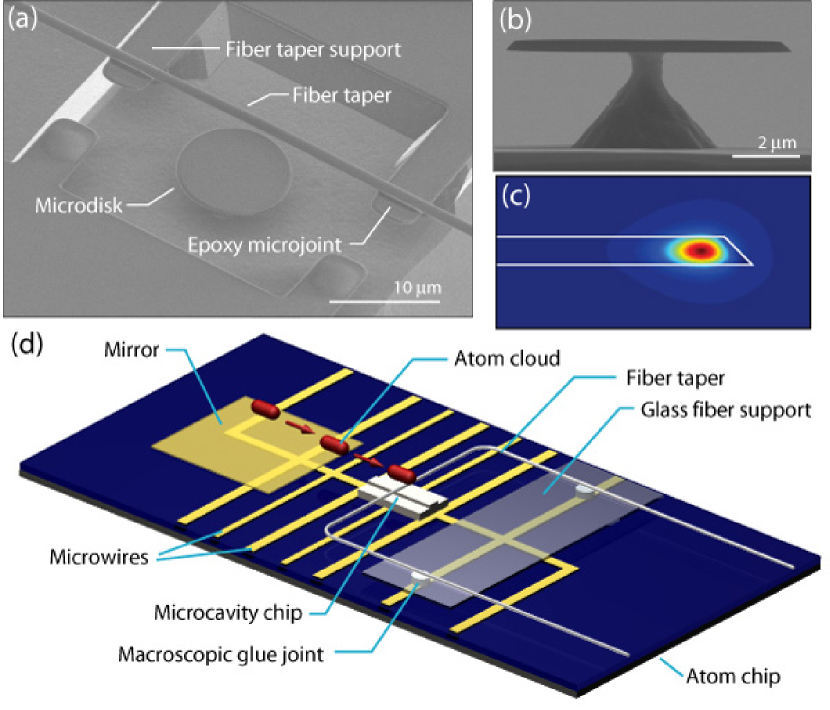
The SiNx microdisk resonators in this work were fabricated from a commercially available Si wafer with a nm thick stoichiometric SiNx () layer grown on the surface by low pressure chemical vapor deposition (LPCVD). Fabrication of the microdisk resonators involved several steps, beginning with the creation of a highly circular electron beam resist etch mask through electron beam lithography and a resist reflowBorselli et al. (2005). A C4F8/SF6 plasma dry etch was optimized to transfer the resist etch mask into the SiNx layer as smoothly as possible. This was followed by a potassium hydroxide wet etch to selectively remove the underlying Si substrate until the SiNx microdisks were supported by a small micron diameter silicon pillar. A final cleaning step to remove organic materials from the disk surface was performed using a H2SO4:H2O2 wet etch. A SEM image of a fully processed microdisk is shown in Fig 1(a,b).
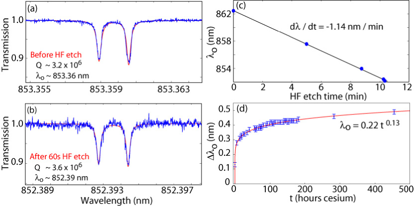
The optical modes of the fabricated microdisks were efficiently excited via an optical fiber taper waveguideKnight et al. (1997); Spillane et al. (2003). A swept wavelength source covering the - nm wavelength band was coupled into the fiber taper waveguide and used to measure the fine transmission spectra of the microdisk resonators at wavelengths close to the D2 transition of cesium (Cs). Details of the fiber taper measurement set-up can be found in Ref. Borselli et al., 2005. Figure 2(a) shows a typical measured wavelength scan of the lowest radial order () TE-like mode of a m diameter SiNx microdisk. The resonance has an intrinsic linewidth of pm, corresponding to a quality factor . The doublet structure in the transmission spectra is due to mode-coupling between the clockwise and counter-clockwise modes of the disk due to surface roughness induced backscatteringKippenberg et al. (2002). In addition to this high- mode, the m microdisks also support a lower higher-order radial mode in the nm wavelength band. The free spectral range between modes of the same radial order but different azimuthal number () was measured to be THz (13 nm), resulting in a finesse of for the , TE-like modes. Tests of less surface sensitive larger diameter microdisks showed reduced doublet splitting but no reduction in linewidth, indicating that is most likely limited by material absorption and not surface roughnessBorselli et al. (2005). This bodes well for utilizing these SiNx microdisks at even shorter wavelengths, such as the nm D2 transition of rubidium.
Finite-element method (FEM) simulationsBorselli et al. (2005) (Fig. 1(c)) show that the effective optical mode volume, defined by , is as small as for the m diameter mirodisks. The corresponding parameters of cavity QED, the Cs-photon coherent coupling rate (), photon field decay rate (), and Cs transverse decay rate () are GHz for an atom at the mircodisk surface, indicating that these cavities are capable of operating well within the regime of strong couplingKimble (1988). For an atom displaced 100 nm from the surface, drops to GHz. FEM simulations show that for microdisks of diameter below m the intrinsic radiation drops rapidly below the level.
Using the above fabrication procedure the resonance wavelength () of the microdisk modes could be positioned with an accuracy of nm. In order to finely tune into alignment with the D2 atomic Cs transition a series of timed etches in 20:1 diluted 49% HF solution was employed. By slowly etching the LPCVD SiNx the resonance wavelength of the high- disk modes was shown to blue shift at a rate of nmmin (Fig. 2(c)). With this technique the cavity resonance could be positioned with an accuracy of nm without degrading the factor (Fig. 2(b)). Further fine tuning can be accomplished by heating and cooling of the sample; a temperature dependence of was measured for the , TE-like microdisk modes.
After initial device characterization and tuning of , the fiber taper and microdisk chip were integrated with an atom chip consisting of a sapphire substrate with electroplated gold microwires underneath a top evaporated gold mirror layerLev (2003); Lev et al. (2004). A brief outline of the integration procedure follows. The 3x3x0.3 mm Si microcavity chip is aligned and bonded to the desired location on the top surface of the atom chip using polymethyl methacrylate. The fiber taper is supported in a self-tensioning “U” configuration by a glass coverslip ( m thick) as illustrated in Fig. 1(d). The taper is aligned with the microdisk using DC motor stages with 50 nm encoder resolution. Adjustment in the lateral gap between the taper and the microdisk is used to tune the level of cavity loading; owing to the excellent phase matching of the fiber taper guided mode to the whispering-gallery modes of the microdiskSpillane et al. (2003) critical coupling was possible with a loaded . The fiber taper and microdisk are then permanently attached using UV curable epoxy in two regions: (i) microscopic glue joints between the fiber taper and lithographically defined SiNx supports (see Fig. 1(a)) fix the position of the taper relative to the disk, and (ii) macroscopic glue joints between the taper support slide and the atom chip (see Fig. 1(d)) fix the position of the taper support relative to the chip and serve as stress relief points for the fiber pigtails. To avoid blocking trapping laser beams or obscuring imaging, the entire fiber taper mount must lie below the plane of the optically and magnetically trapped atoms ( m above the atom chip surface). A sufficiently low-profile is achieved by aligning and bonding the taper support glass coverslip parallel to and below the plane of the microdisk chip top surface. During the taper mounting procedure the taper-microdisk coupling is monitored by measuring and the transmission contrast (), with no noticable change being observed during the curing of the epoxy joints. The micro glue joints incur a taper diameter dependent amount of broadband insertion loss; for the taper diameters used here ( m) an approximate - optical loss per joint is typical. Post-cure, the fiber-cavity alignment is extremely robust, withstanding all of the vacuum installation procedures described below.
The integrated atom-cavity chip was installed in an ultra-high vacuum (UHV) chamber designed for performing atom chip waveguiding experiments. Vacuum-safe fiber feedthroughsAbraham and Cornell (1998) were used to pass the fiber-pigtails out of the chamber. The chamber was evacuated using turbo and ion pumps and baked at 130 C for hours so that a background pressure of Torr was reached. Initial experiments with the integrated system involved the trapping of Cs atoms in a mirror-MOTReichel (2002) above the atom chip gold mirror and transfer of atoms to a micro-U-MOT Reichel (2002) for subsequent magnetic trapping and guiding on the atom chip (see Fig. 1(d)). The extremely low-profile of the fiber taper mounting was shown to provide excellent optical access for atom trapping, cooling, and imaging. The microdisk resonance was continuously monitored during these procedures. was found to remain constant during the chamber pump-down, bake-out, and atom trapping, demonstrating the robustness of the fiber-cavity mounting. However, after the chamber bake, was red shifted nm from the pre-bake value and was found to increase logarithmically with exposure time to the Cs vapor as shown in Fig. 2(d). During subsequent chamber bakes and intermittent closures of the Cs source (for periods as long as 2 weeks) was found to remain constant.
The logarithmic time dependence of with Cs exposure suggests that the Cs coverage of the microdisk surface is saturating in a “glassy” manner Palmer et al. (1984); interactions between deposited atoms quench the rate of adsorption. A shift of the disk resonances can be related to a surface film thickness by , where represents the fraction of modal energy in the film and is the refractive index of the film. From finite element simulations of the microdisk, nm-1 for the TE-like mode. Assuming a film index of refraction equal to that of SiNx, the measured wavelength shift at the longest measured time ( h) corresponds to roughly a half-monolayer coverage of Cs on the disk surface (monolayer thickness Brause et al. (1997)).
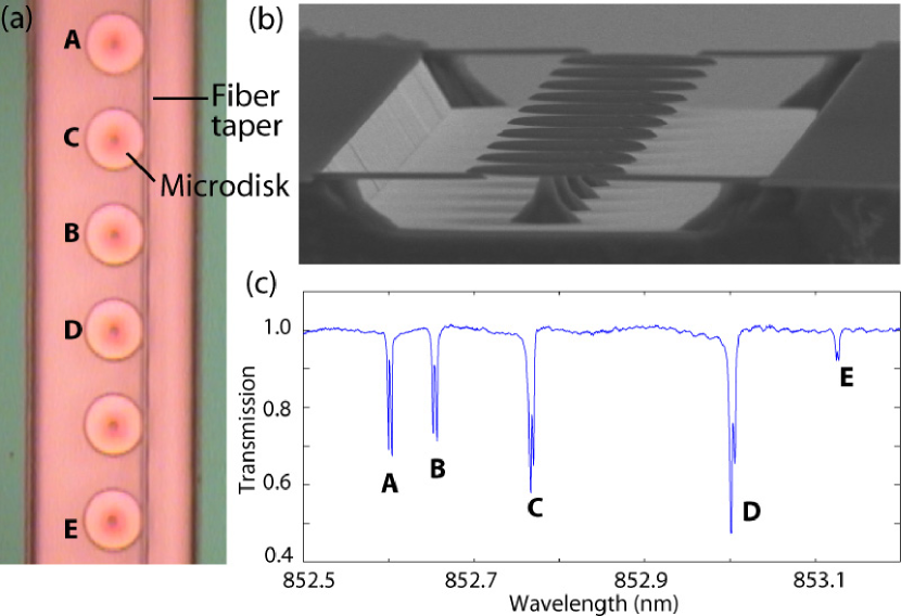
As a future method of compensating for resonant detuning of the microdisk mode due to variation in fabrication or the time-dependent Cs surface coverage, and as an initial demonstration of the scalability of the fiber-coupled microdisk chip concept, we show in Figure 3(a) a single fiber taper coupled in parallel to an array of 10 nominally identical microdisks (Fig. 3(b)). Over a nm wavelength range the fiber taper couples to 5 of the , TE-like modes as shown in Fig. 3(c), the remaining 5 modes lying within a nm range. A modest 10 C of temperature tuning may be used to tune between the 5 closely spaced modes. Each of these resonances is due to coupling to a unique microdisk, as verified by imaging the scattered light from the microdisks as a function of wavelength.
In conclusion, we have shown that wavelength-scale high- microcavities can be realized from SiNx at near-visible wavelengths, and have demonstrated a method for integrating these devices with atom chips. The resulting optical fiber taper interface to the hybrid atom-cavity chip provides sufficient optical access for chip-based atom trapping and cooling while providing highly efficient optical coupling to single, or simultaneously to multiple, microdisk cavities. In the future, the use of SiNx microcavities provides a path to a fully monolithic atom-cavity Si chip.
The authors thank M. Borselli and T. Johnson for assistance in FEM simulations and microdisk process development, and J. Kerckhoff for help with Cs adsorbtion measurements.
References
- Reichel (2002) J. Reichel, Appl. Phys. B 74, 469 (2002).
- Folman et al. (2002) R. Folman, P. Krüger, J. Schmiedmayer, J. Denschlag, and C. Henkel, Ad. Mod. Phys. 48, 263 (2002).
- Vahala (2003) K. J. Vahala, Nature 424, 839 (2003).
- Song et al. (2005) B.-S. Song, S. Noda, T. Asano, and Y. Akahane, Nat. Mat. 4, 207 (2005).
- Armani et al. (2003) D. K. Armani, T. J. Kippenberg, S. M. Spillane, and K. J. Vahala, Nature 421, 925 (2003).
- Kimble (1988) H. J. Kimble, Phys. Scr., T T76, 127 (1988).
- Duan and Kimble (2004) L. M. Duan and H. J. Kimble, Phys. Rev. Lett. 12, 127902 (2004).
- Lev et al. (2004) B. Lev, K. Srinivasan, P. E. Barclay, O. Painter, and H. Mabuchi, Nanotechnology 15, S556 (2004).
- Haase et al. (2006) A. Haase, B. Hessmo, and J. Schmiedmayer, Opt. Lett. 31, 268 (2006).
- Rosenblit et al. (2004) M. Rosenblit, P. Horak, S. Helsby, and R. Folman, Phys. Rev. A 70, 053808 (2004).
- McKeever et al. (2004) J. McKeever, A. Boca, A. D. Boozer, R. Miller, J. R. Buck, A. Kuzmich, and H. J. Kimble, Science 303, 1992 (2004).
- Groth et al. (2004) S. Groth, P. Krüger, S. Wildermuth, R. Folman, T. Fernholz, J. Schmiedmayer, D. Mahalu, and I. Bar-Joseph, Appl. Phys. Lett. 85, 2980 (2004).
- Parsons et al. (1991) G. N. Parsons, J. H. Souk, and J. Batey, J. Appl. Phys. 70, 1553 (1991).
- Inukai and Ono (1994) T. Inukai and K. Ono, Jpn. J. Appl. Phys. 33, 2593 (1994).
- Little et al. (2004) B. E. Little, S. T. Chu, P. P. Absil, J. V. Hryniewicz, F. Seiferth, D. Gill, V. Van, O. King, and M. Traklo, IEEE Photonics Tech. Lett. 16, 2263 (2004).
- Barwicz et al. (2004) T. Barwicz, M. A. Popovic, P. T. Rakich, M. R. Watts, H. A. Haus, E. P. Ippen, and H. I. Smith, Opt. Expr. 12, 1437 (2004).
- Netti et al. (2000) M. C. Netti, M. D. B. Charlton, G. J. Parker, and J. J. Baumberg, Appl. Phys. Lett. 76, 991 (2000).
- Vollmer et al. (2002) F. Vollmer, D. Braun, A. Libchaber, M. Khoshsima, I. Teraoka, and S. Arnold, Appl. Phys. Lett. 80, 4057 (2002).
- Ksendzov et al. (2004) A. Ksendzov, M. L. Homer, and A. M. Manfreda, IEE Elec. Lett. 40, 63 (2004).
- Borselli et al. (2005) M. Borselli, T. J. Johnson, and O. Painter, Opt. Expr. 13, 1515 (2005).
- Knight et al. (1997) J. Knight, G. Cheung, F. Jacques, and T. Birks, Opt. Lett. 22, 1129 (1997).
- Spillane et al. (2003) S. M. Spillane, T. J. Kippenberg, O. J. Painter, and K. J. Vahala, Phys. Rev. Lett. 91, 043902 (2003).
- Kippenberg et al. (2002) T. J. Kippenberg, S. M. Spillane, and K. J. Vahala, Opt. Lett. 27, 1669 (2002).
- Lev (2003) B. Lev, Quantum Information and Computation 3, 450 (2003).
- Abraham and Cornell (1998) R. I. Abraham and E. A. Cornell, Appl. Opt. 37, 1762 (1998).
- Palmer et al. (1984) R. G. Palmer, D. L. Stein, E. Abrahams, and P. W. Anderson, Phys. Rev. Lett. 53, 958 (1984).
- Brause et al. (1997) M. Brause, D. Ochs, J. Günster, T. Mayer, B. Braun, V. Puchin, W. Maus-Friedrichs, and V. Kempter, Surf. Sci. 383, 216 (1997).