Pulse-induced acoustoelectric vibrations in surface-gated GaAs-based quantum devices
Abstract
We present the results of a numerical investigation which show the excitation of acoustoelectric modes of vibration in GaAs-based heterostructures due to sharp nano-second electric-field pulses applied across surface gates. In particular, we show that the pulses applied in quantum information processing applications are capable of exciting acoustoelectric modes of vibration including surface acoustic modes which propagate for distances greater than conventional device dimensions. We show that the pulse-induced acoustoelectric vibrations are capable of inducing significant undesired perturbations to the evolution of quantum systems.
pacs:
85.35.Gv, 73.23.-b, 77.65.DqINTRODUCTION
Quantum computers have the potential to efficiently solve “hard problems”, for which there are no known efficient classical algorithms NielsonBook . The realization of a quantum processor is currently a major challenge at the forefront of experimental physics. Semiconductor quantum dots form the basis of many solid-state devices being developed for the implementation of quantum logic gates. They are believed to be promising candidates for producing scalable systems, as they take advantage of the technology available for the fabrication of semiconductor technology. The essential requirements for the realization of such devices are the coherent manipulation of an electronic degree of freedom in each dot and the control of coupling between adjacent dots. Since the theoretical work of Loss and DiVincenzo Loss:98 , experimental progress has been made in the realization of spin qubits Petta:05 and charge qubits Hayashi:04 based on quantum dots formed by the surface gating of a two-dimensional electron gas (2DEG) where voltage pulses are used to control exchange interaction and tunnelling, respectively, between adjacent dots. However, the scaling of such systems requires the identification and minimization of the decoherence processes, which arise from the coupling of the quantum dot to its environment. This requires a precise understanding of the dynamical evolution of both the relevant electronic degree of freedom and the environment to which it is coupled.
In our recent theoretical work Rahman:05:1 ; Rahman:05:2 , we had implemented mechanical boundary conditions in the form of time-dependent traction forces on the surface of a GaAs-based device, to excite acoustoelectric vibrations. By utilizing the piezoelectric nature of GaAs, time-varying electric fields form the basis of surface acoustic wave generation through interdigitated transducers. The time-varying electric fields such as those used to manipulate spin and charge qubits in quantum information processing applications may also excite acoustoelectric vibrations. These vibrations would be undesirable for the operation of sensitive quantum dot systems.
In this paper, we show through the numerical solution of the equations of motion in GaAs, the excitation of acoustoelectric modes of vibration in GaAs-based heterostructure devices, due to pulsed electric fields. We discuss the results in relation to the construction of scalable quantum dot devices.
THEORY
The equations of motion in a general piezoelectric material are Auld
| (1) |
| (2) |
where is a displacement vector, is the electrostatic potential field, are components of the elastic tensor, are components of the material dielectric (the superscripts E and S indicate measurements under constant strain and electric field respectively), is the mass density, and are components of the piezoelectric tensor.
The mechanical boundary conditions require the prescription of the traction forces at each external surface, where is a unit vector perpendicular to an external surface, and are components of the stress tensor, defined by
| (3) |
where and . The electrostatic boundary conditions require the prescription of the normal component of the electric displacement at the free surface of the medium. The electric displacement vector is defined by
| (4) |
The equations consist of a system of coupled linear partial differential equations second order in space and time. The solution of these equations for non-trivial boundary conditions requires numerical methods. Our numerical solution method, which utilizes a finite element approximation for the spatial part and a second order finite difference discretisation in time, is suitable for the simulation of electromechanical waves Rahman:05:1 . We have used eight-noded brick elements corresponding to linear basis functions , resulting in an overall spatial and temporal convergence rate of 2 for the error. An operator splitting strategy is employed to split the coupled - problem DpBook2 . The numerical formulation and verification is described in more detail in Ref. Rahman:05:1, .
For GaAs, the non-zero components of the piezoelectric tensor have the value Cm-2. The non-vanishing components of the permittivity tensor are ( Fm-1), and the non-vanishing components of the elastic tensor are = = = = Nm-2, = = = = Nm-2, and = = = = Nm-2. All other non-zero components of the elasticity tensor can be determined by applying its symmetry properties . The mass density of GaAs has the value of Kgm-3 Adachi .
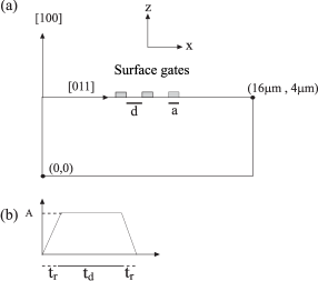
Figure 1(a) shows a schematic representation of the system we have modelled in our simulations. The coordinate and -axes are aligned with the crystal [011] and [100] directions, respectively, as is frequently the case in the realization of GaAs-based quantum dot systems. For this orientation, the properties of acoustoelectric vibrations are well documented Simon ; Rahman:05:2 and hence it is also convenient for the interpretation of our results.
The anisotropic nature of GaAs will result in some dependence of the acoustic properties on the crystal orientation. However, this is expected to be small as the components of the piezoelectric tensor are equal and the components of the elasticity tensor are the same order of magnitude. In general, quantum dot applications will include electric fields across components in the orientation investigated in this paper. The presence of a thin layer of AlGaAs is neglected for simplicity, and has been shown to have little effect on the acoustic properties Rahman:05:2 . As in our previous work we avoid a Hartree-Fock type self-consistent calculation as the benefits of this are likely to be small compared to drawbacks associated with vast computational resources.
In our simulations, we implement a trapezoidal form for the applied voltage pulse as shown in Fig. 1(b). Trapezoidal pulses are implemented in experiments where coherent manipulation or measurement of single electron charge and spin -systems have been achieved Hayashi:04 ; Elzerman:04 ; Petta:05 . Figure 1(b) shows the geometrical features of the pulse. In experimental demonstrations, the parameters of the pulse are such that , . We apply the voltage bias to the central gate relative to the outer gates. The gate width and separation are chosen to be those frequently used in experiments to define quantum dots; nm nm. The mechanical gates are excluded from our simulations as they are capable of perturbing the induced vibrations Rahman:05:2 . The presence of mechanical gates has been shown to reduce the amplitude of surface acoustic modes but also affect its vibrational frequency. To model the applied voltage bias, we apply Dirichlet boundary conditions on the regions of the surface which the gates would occupy and a Neumann-type condition elsewhere through setting ft0 . For the mechanical boundary conditions, we apply traction-free boundary conditions i.e. on the external surfaces.
The precise characterization of the dependence of the effects of a pulse on all the parameters of this system is beyond the scope or intention of this paper. Our aim is to show the effects on the underlying lattice of electric-field pulses frequently used in quantum dot experiments. We first demonstrate the effects of a “typical” pulse used in experiments, and then consider the dependence of these effects on the parameters of the applied pulse, and .
RESULTS AND DISCUSSIONS
Figure 2(a) shows the oscillations of the electric potential , along the axis and nm below the surface (as this is the standard depth of a 2DEG), resulting from a pulse with V, ns and ns. From time ns, the waves propagate outward from the center at velocities ranging from ms-1 to ms-1, with the lower velocities likely to correspond to surface acoustic waves Simon and the higher velocities to other modes which include bulk waves.
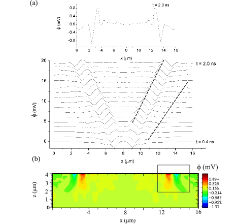
As the inset of Fig. 2(a) shows, the maximum amplitude of the waves at the time ns is mV. The linearity of the underlying equations of motion would require a linear relationship between the amplitude of the applied pulse, and that of the pulse induced oscillations. The pulse induced vibrations are small compared to the direct electrostatic coupling as well as relevant electrical characteristics of conventional quantum dot devices including the charging energy and energy-level spacings. In particular, the pulse-induced vibrations would be screened in the conductive regions. However, in the unscreened or depleted regions, the pulse induced vibrations will be visible. Of particular relevance, is in applications where electrical pulses are implemented to align electronic energy levels between a lead and a single quantum dot or between adjacent quantum dots. In such systems, the pulse-induced vibrations could momentarily perturb the alignment and lead to uncertainty in the evolution in the electronic system.
Moreover, surface acoustic waves with amplitudes less than mV have proved to provide an efficient means of implementing quantized charge pumping Ebbecke:03 .
The acoustic vibrations could be described as phonons which have been shown in experiment Fujisawa:00 and theory Brandes:99 to couple strongly to electrons. When the energy level separations in a quantum dot are equal to the energies of the excited phonons, the phonons could be absorbed by electrons in the dot. In a double quantum dot system, this could lead to inelastic tunnelling between the adjacent dots Naber:06 .
Figure 2(a) also shows the ability of the surface acoustic wave modes to propagate for at least four microns along the surface with no decay in amplitude. The mentioned four microns is only a limit of the computational domain and we would expect the induced surface acoustic wave to propagate over much longer distances. Figure 2(b) shows grayscale plots of the induced electrical potential at time ns. The stronger potential fields at (m) and (m) are clearly localized at the surface (i.e. m) with the amplitude at two wavelengths into the depth (V) substantially reduced compared to that at the surface ( mV), as is characteristic of surface acoustic waves in GaAs.
In the experimental realization of quantum information processing devices Hayashi:04 ; Petta:05 the applied voltage pulses are of the order of mV. Our simulations predict the excitation of surface acoustic waves with amplitudes of V, which is comparable to the inelastic tunnelling energies and the energy level bias applied to a double dot system Hayashi:04 ; ft1 . To demonstrate an effect of this pulsed-induced surface acoustic wave on a adjacent double quantum dot system, we solve numerically the relevant time-dependent Schrödinger equation;
| (5) |
where is the energy difference between the uncoupled localized states, is the energy difference between the stationary states when the local charge states are degenerate, and are the Pauli matrices. In our calculation, is computed by assuming that the quantum dot centers of the adjacent system are separated by a distance of nm Hayashi:04 , and have a zero energy-level bias in the absence of acoustoelectric vibrations. This double-dot is located m laterally away from the source of surface acoustic waves. We compare the state of the neighboring double-dot system with and without the electric potential wave, to determine the influence of the acoustic vibrations. Figure 3 shows the infidelity between the states, as a function of chosen to correspond to that in experiments (and is assumed constant for simplicity) Hayashi:04 .

The oscillations of Fig. 3 approximately commensurate with the frequency of the acoustic vibrations ( GHz). The infidelity oscillates between and which corresponds to a substantial perturbation to the evolution of the quantum state. This result is simply representative of what may happen, showing that significant errors can occur for typical parameters and that a judicious choice of parameters can mitigate the error.
In a system consisting of an array of quantum dots on the surface, each of which implements electric-field pulses to control an electronic degree of freedom, we would expect the excitation of surface acoustic waves, which would be capable of traversing through multiple quantum dots. The necessity to incorporate the information regarding the electric-field pulses applied to every quantum dot, into the description of the dynamics of each quantum dot, potentially poses a significant challenge for the scalability of these systems for quantum information processing applications.
In addition, the readout of the final state of a quantum system requires the preparation, manipulation and measurement of an ensemble of identically prepared systems and hence, the repeated application of an electrical pulse. As a result, we could expect a substantial accumulation of acoustoelectric vibrations within the underlying lattice.
The dependence of the pulse-induced acoustoelectric vibrations, on the duration of the pulse is investigated by varying from ns to ns, with ns and mV. The measurements correspond to ns after the end of the pulse train. Figure 4(a) shows the computed root mean square () and maximum of the modulus () of the induced oscillations computed at nm below the surface for data between nm and m, for each value of . Both measures are included as the takes into account all wave modes (surface and bulk) whereas from the we see the maximum amplitude i.e. only the surface mode. One can see a rapid increase of these measures up to ns, after which the becomes flat at mV, while the measure stabilizes at mV. The dramatic change in behavior at ns, can be understood by examining the deformation of the underlying lattice. Figure 4(b) shows the component of the lattice displacement as the voltage pulse is applied. The component exhibits similar behavior is not therefore shown. As an external electric-field pulse is applied, the lattice slowly deforms. After a certain amount of time (with the voltage bias on), the lattice deformation reaches its equilibrium value (for the given electric potential), and then oscillates about this position before stabilizing. The time is ns for the device modelled in this work. We would expect the time to depend on the material, the device geometry, crystal orientation with respect to the coordinate axes and the model for the applied electric field (which in our case avoids a full self-consistent calculation).
In our simulations, the response time of the lattice to the applied electric fields is much greater than the frequently applied rise times of the applied pulse which in the ideal case is zero. Hence, for the regime of interest in semiconductor quantum dot applications, variation of the rise time of the pulse would have little effect on the pulsed-induced vibrations.
We may also conclude from our investigations of varying the rise time and duration of the pulse, that the pulses implemented in quantum information processing applications excite acoustoelectric vibrations of the maximum amplitude (for a given amplitude for the applied pulse).
Future work may involve the investigation of novel schemes which may reduce the effect of the acoustoelectric vibrations. For the present time, we point out that surface acoustic waves may be utilized for quantum information processing applications Barnes:00 . Moreover, materials which have a spatial inversion center such as Si are immune to the excitation of acoustoelectric vibrations through electric field pulses and thus have a significant advantage for quantum control and quantum computation. Devices based on such materials are currently being developed for quantum computation Gorman:05 ; Rahman:05:3 ; Kane:98 .
Many spin-readout proposals rely on mapping a spin state to a charge state, since the detectors that are likely to be used are Quantum Point Contacts (QPC’s). Therefore, the results are also relevant to spin qubit systems Barrett:06 ; Stace:04 .

CONCLUSION
In conclusion, we have demonstrated the excitation of acoustoelectric modes of vibration in a GaAs lattice as a result of sharp nano-second electric-field pulses applied to surface gates. The excited wave modes include surface acoustic modes which have been shown to travel at least four microns along the free surface of a material. We have demonstrated the substantial perturbation these waves may have on the evolution of quantum systems. Whilst the effect we have considered does not decohere the system in the normal sense of becoming correlated with the environment, the fact the acoustoelectric waves induced by gates at one place can significantly affect the state of a remote double-dot system, means that the results are very significant for quantum information processing applications.
ACKNOWLEDGEMENTS
We thank T. Fujisawa, T. Hayashi, C. M. Marcus, C. J. B. Ford, J. Jefferson, R. Young and S. Pfaendler for comments, useful discussions and assistance. SR acknowledges the Cambridge-MIT Institute for financial support.
References
- (1) M. A. Nielsen and I. L. Chuang, Quantum Computation and Quantum Information, Cambridge University Press, (2003).
- (2) D. Loss and D. P. DiVincenzo, Phys. Rev. A 57, 120 (1998).
- (3) J. R. Petta, A. C. Johnson, J. M. Taylor, E. A. Laird, A. Yacoby, M. D. Lukin, C. M. Marcus, M. P. Hanson and A. C. Gossard, Science 309, 2180, (2005).
- (4) T. Hayashi, T. Fujisawa, H. D. Cheong, Y. H. Jeong and Y. Hirayama, IEEE Trans. Nanotech. 3, 300, (2004); Phys. Rev. Lett. 91, 226804, (2003).
- (5) S. Rahman, H. P. Langtangen, and C. H. W. Barnes, Commun. Comput. Phys. 2, 271 (2006).
- (6) S. Rahman, M. Kataoka, C. H. W. Barnes and H. P. Langtangen, Phys. Rev. B 74, 035308, (2006).
- (7) J. M. Elzerman, R. Hanson, L. H. Willems van Beveren, B. Witkamp, L. M. K. Vandersypen and L. P. Kouwenhoven, Nature 430, 431, (2004).
- (8) B. A. Auld, Acoustic Waves and Fields in Solids, vol. 1, Wiley (1973).
- (9) H. P. Langtangen, Computational Partial Differential Equations – Numerical Methods and Diffpack Programming, Springer, 2nd edition (2003).
- (10) S. Adachi, Properties of Aluminium Gallium Arsenide, Institution of Electrical Engineers (1993).
- (11) S. H. Simon, Phys. Rev. B 54, 13878 (1996).
- (12) When air is considered above the substrate, the boundary condition consists of the continuity of . The present boundary condition is useful when air is neglected for computational speed.
- (13) J. Ebbecke, N. E. Fletcher, T. J. B. M. Janssen, F. J. Ahlers, M. Pepper, H. E. Beere and D. A. Ritchie, Appl. Phys. Lett. 84, 4319 (2004).
- (14) T. Fujisawa, W. G. van der Wiel and L. P. Kouwenhoven, Physica E 7, 413, (2000).
- (15) T. Brandes and B. Kramer, Phys. Rev. Lett. 83, 3021 (1999).
- (16) W. J. M. Naber, T. Fujisawa, H. W. Liu and W. G. van der Wiel, Phys. Rev. Lett. 96, 136807, (2006).
- (17) We have performed simulations which suggest that variation of the gate width within the quantum dot regime, does not have a significant effect on the amplitude of the induced vibrations.
- (18) C. H. W. Barnes, J. M. Shilton, and A. M. Robinson, Phys. Rev. B 62, 8410, (2000).
- (19) J. Gorman, D. G. Hasko and D. A. Williams, Phys. Rev. Lett. 95, 090502 (2005).
- (20) S. Rahman, J. Gorman, C. H. W. Barnes, D. A. Williams and H. P. Langtangen, Phys. Rev. B 73, 233307, (2006).
- (21) B. E. Kane, Nature 393, 133 (1998).
- (22) S. D. Barrett and T. M. Stace, Phys. Rev. B 73, 075324 (2006).
- (23) T. M. Stace, S. D. Barrett, H-S. Goan, and G. J. Milburn, Phys. Rev. B 70, 205342, (2004).