Spin Decoherence in Superconducting Atom Chips
Abstract
Using a consistent quantum-mechanical treatment for the electromagnetic radiation, we theoretically investigate the magnetic spin-flip scatterings of a neutral two-level atom trapped in the vicinity of a superconducting body. We derive a simple scaling law for the corresponding spin-flip lifetime for such an atom trapped near a superconducting thick slab. For temperatures below the superconducting transition temperature , the lifetime is found to be enhanced by several orders of magnitude in comparison to the case of a normal conducting slab. At zero temperature the spin-flip lifetime is given by the unbounded free-space value.
pacs:
34.50.Dy, 03.75.Be, 42.50.CtCoherent manipulation of matter waves is one of the ultimate goals of atom optics. Trapping and manipulating cold neutral atoms in microtraps near surfaces of atomic chips is a promising approach towards full control of matter waves on small scales folman_02 . The subject of atom optics is making rapid progress, driven both by the fundamental interest in quantum systems and by the prospect of new devices based on quantum manipulations of neutral atoms.
With lithographic or other surface-patterning processes complex atom chips can be built which combine many traps, waveguides, and other elements, in order to realize controllable composite quantum systems zoller_00 as needed, e.g., for the implementation of quantum information devices divin_00 . Such microstructured surfaces have been highly successful and form the basis of a growing number of experiments hommelhoff_05 . However, due to the proximity of the cold atom cloud to the macroscopic substrate additional decoherence channels are introduced which limit the performance of such atom chips. Most importantly, Johnson noise currents in the material cause electromagnetic field fluctuations and hence threaten to decohere the quantum state of the atoms. This effect arises because the finite temperature and resistivity of the surface material are always accompanied by field fluctuations, as a consequence of the fluctuation-dissipation theorem. Several experimental hinds_03 ; vuletic_04 ; harber_03 as well as theoretical henkel_99 ; dung_00 ; rekdal_04 ; scheel_05 studies have recently shown that rf spin-flip transitions are the main source of decoherence for atoms situated close to metallic or dielectric bodies. Upon making spin-flip transitions, the atoms become more weakly trapped or even lost from the microtrap.
In Ref. rekdal_04 it was shown that to reduce the spin decoherence of atoms outside a metal in the normal state, one should avoid materials whose skin depth at the spin-flip transition frequency is comparable with the atom-surface distance. For typical values of these parameters used in experiments, however, this worst-case scenario occurs hinds_03 ; vuletic_04 ; harber_03 . To overcome this deficiency, it was envisioned scheel_05 that superconductors might be beneficial in this respect because of their efficient screening properties, although this conclusion was not backed by a proper theoretical analysis. It is the purpose of this letter to present a consistent theoretical description of atomic spin-flip transitions in the vicinity of superconducting bodies, using a proper quantum-mechanical treatment for the electromagnetic radiation, and to reexamine Johnson-noise induced decoherence for superconductors. We find that below the superconducting transition temperature the spin-flip lifetime becomes boosted by several orders of magnitude, a remarkable finding which is attributed to: (1) the opening of the superconducting gap and the resulting inability to deposit energy into the superconductor, (2) the highly efficient screening properties of superconductors, and (3) the small active volume within which current fluctuations can contribute to field fluctuations. Our results thus suggest that current-noise induced decoherence in atomic chips can be completely diminished by using superconductors instead of normal metals.
We begin by considering an atom in an initial state and trapped at position in vacuum, near a dielectric body. The rate of spontaneous and thermally stimulated magnetic spin-flip transition into a final state has been derived in Ref. rekdal_04 ,
| (1) | |||||
Here is the Bohr magneton, is the electron spin factor, is the matrix element of the electron spin operator corresponding to the transition , and is the dyadic Green tensor of Maxwell’s theory. Eq. (1) follows from a consistent quantum-mechanical treatment of electromagnetic radiation in the presence of absorbing bodies dung_00 ; henry_96 . Thermal excitations of the electromagnetic field modes are accounted for by the factor , where is the mean number of thermal photons per mode at frequency of the spin-flip transition. The dyadic Green tensor is the unique solution to the Helmholtz equation
with appropriate boundary conditions. Here is the wavenumber in vacuum, is the speed of light and the unit dyad. This quantity contains all relevant information about the geometry of the material and, through the electric permittivity , about its dielectric properties.
The current density in superconducting media is commonly described by the Mattis Bardeen theory mattis_58 . To simplify the physical picture, let us limit the discussion to low but non-zero frequencies , where is the angular frequency and is the energy gap of the superconductor at zero temperature. In this limit, the current density is well described by means of a two-fluid model gorter_34 ; london_34_40 . At finite temperature , the current density consists of two types of electrons, superconducting electrons and normal conducting electrons. The total current density is equal to the sum of a superconducting current density and a normal conducting current density, i.e. . Let us furthermore assume that the superconducting as well as the normal conducting part of the current density responds linearly and locally to the electric field remark_local , in which case the current densities are given by the London equation and Ohm’s law, respectively,
| (3) |
The London penetration length and the normal conductivity are given by,
| (4) |
Here is the electrical conductivity of the metal in the normal state, is the electron mass, is the electron charge, and and are the electron densities in the superconducting and normal state, respectively, at a given temperature . Following London london_34_40 , we assume that the total density is constant and given by , where for and for . For a London superconductor with the assumptions as mentioned above, the dielectric function in the low-frequency regime reads
| (5) |
where is the skin depth associated with the normal conducting electrons. The optical conductivity corresponding to Eq. (5) is .
In the following we apply our model to the geometry shown in Fig. 1, where an atom is located in vacuum at a distance away from a superconducting slab. We consider, in correspondence to recent experiments vuletic_04 ; harber_03 ; hinds_03 , 87Rb atoms that are initially pumped into the state. Fluctuations of the magnetic field may then cause the atoms to evolve into hyperfine sublevels with lower . Upon making a spin-flip transition to the state, the atoms are more weakly trapped and are largely lost from the region of observation, causing the measured atom number to decay with rate associated with the rate-limiting transition . The transition rate can be decomposed into a free part and a part purely due to the presence of the slab. The free-space spin-flip rate at zero temperature is rekdal_04 . The slab-contribution can be obtained by matching the electromagnetic fields at the vacuum-superconductor interface. With the same spin-orientation as in Ref.scheel_05 , i.e. and , the spin-flip rate is , with the atom-spin orientation dependent integrals
| (6) | |||||
| (7) |
and the electromagnetic field polarization dependent Fresnel coefficients
| (8) |
Here we have and . In particular, above the transition temperature the dielectric function in Eq. (5) reduces to the well known Drude form. Due to the efficient screening properties of superconductors, in most cases of interest the inequality holds. Assuming furthermore the near-field case , where is the wavelength associated to the spin-flip transition, which holds true in practically all cases of interest, we can compute the integrals in Eqs. (6–8) analytically to finally obtain
| (9) |
For a superconductor at , in which case there are no normal conducting electrons, it is seen from Eq. (9) that the lifetime is given by the unbounded free-space lifetime .
Eq. (9) is the central result of our paper. To inquire into its details, we compute the spin-flip rate for the superconductor niobium (Nb) and for a typical atomic transition frequency kHz hinds_03 . We keep the atom-surface distance fixed at m, and use the Gorter-Casimir gorter_34 temperature dependence
| (10) |
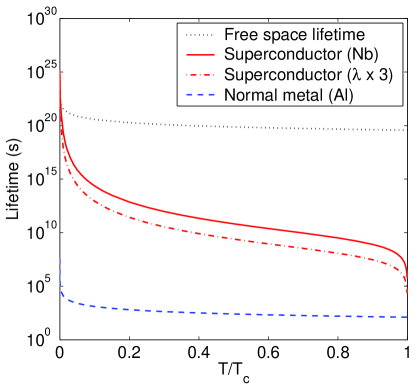
for the superconducting electron density. Figure 2 shows the spin-flip lifetime of the atom as a function of temperature: over a wide temperature range remains as large as seconds. In comparison to the normal-metal lifetime , which is obtained for aluminum with its quite small skin depth m and using the results of Refs. rekdal_04 ; scheel_05 , we observe that the lifetime becomes boosted by almost ten orders of magnitude in the superconducting state. In particular, for the ratio between and is even . From the scaling behavior (9) we thus observe that decoherence induced by current-fluctuations in the superconducting state remains completely negligible even for small atom-surface distances around 1 m, in strong contrast to the normal state where such decoherence would limit the performance of atomic chips.
The scaling behavior of the spin-flip rate (9) can be understood qualitatively on the basis of Eq. (1). The fluctuation-dissipation theorem dung_00 ; henry_96 relates the imaginary part of the Green tensor and by , assuming a suitable real-space convolution, and allows to bring the scattering rate Eq. (1) to a form reminiscent of Fermi’s golden rule. The magnetic dipole of the atom at couples to a current fluctuation at point in the superconductor through . The propagation of the current fluctuation is described by the dielectric function , and finally a back-action on the atomic dipole occurs via . For the near-field coupling under consideration, , the dominant contribution of the Green tensor is , thus resulting in the overall dependence of the spin-flip rate (9). The imaginary part of the dielectric function (5) accounts for the loss of electromagnetic energy to the superconductor, and is only governed by electrons in the normal state, whereas electrons in the superconducting state cannot absorb energy because of the superconducting gap. Finally, the term is due to the dielectric screening of the charge fluctuation seen by the atom, and an additional contribution associated to the active volume of current fluctuations which contribute to the magnetic field fluctuations at the position of the atom. Fluctuations deeper inside the superconductor are completely screened out. In comparison to the corresponding scaling for a normal metal scheel_05 , which can be qualitatively understood by a similar reasoning, the drastic lifetime enhancement in the superconducting state is thus due to the combined effects of the opening of the superconducting gap, the highly efficient screening, and the small active volume.
Let us finally briefly comment on the validity of our simplified approach, and how our results would be modified if using a more refined theory for the description of the superconductor. Our theoretical approach is valid in the same parameter regime as London’s theory, that is . It is well known that nonlocal effects modify the London length in Nb from nm to nm miller_59 , and the coherence length , according to Pippard’s theory pippard_53 , from the BCS value to , where is of the order one and is the mean free path. For Nb, nm and nm pronin_98 , and the London condition is thus satisfied. Furthermore, at the atomic transition frequency the conductivity is casalbuoni_05 and the corresponding skin depth is , such that Ohm’s law is also valid since reuter_48 . It is important to realize that other possible modifications of the parameters used in our calculations will by no means change our findings, which only rely on the generic superconductor properties of the efficient screening and the opening of the energy gap, and that our conclusions will also prevail for other superconductor materials.
We also mention that for both a superconductor at and a perfect normal conductor, i.e. , the lifetime is given by the unbounded free-space lifetime . In passing, we notice that for an electric dipole transition and for a perfect normal conductor, as e.g discussed in Refs.knight_73 , the correction to the vacuum rate is in general opposite in sign as compared to that of a magnetic dipole transition. Elsewhere decay processes in the vicinity of a thin superconducting film will discussed in detail rekdal_07 .
To summarize, we have used a consistent quantum theoretical description of the magnetic spin-flip scatterings of a neutral two-level atom trapped in the vicinity of a superconducting body. We have derived a simple scaling law for the corresponding spin-flip lifetime for a superconducting thick slab. For temperatures below the superconducting transition temperature , the lifetime has been found to be enhanced by several orders of magnitude in comparison to the case of a normal conducting slab. We believe that this result represents an important step towards the design of atomic chips for high-quality quantum information processing.
We are grateful to Heinz Krenn for helpful discussions. Work supported in part by the Austrian Science Fund (FWF).
References
- (1) R. Folman, P. Krueger, J. Schmiedmayer, J. Denschlag, and C. Henkel, At. Mol. Opt. Phys. 48, 236 (2002).
- (2) P. Zoller, Nature 404, 236 (2002).
- (3) D. P. DiVincenzo, Fortschr. Phys. 48, 771 (2000).
- (4) P. Hommelhoff, W. Häsel, T. W. Hänsch, and J. Reichel New Journ. Phys. 7, 3 (2005).
- (5) M.P.A. Jones, C.J. Vale, D. Sahagun, B.V. Hall, and E.A. Hinds, Phys. Rev. Lett. 91, 080401 (2003).
- (6) Y.J. Lin, I. Teper, C. Chin, and V. Vuletic, Phys. Rev. Lett. 92, 050404 (2004);
- (7) D.M. Harber, J.M. McGuirk, J.M. Obrecht, and E.A. Cornell, J. Low. Temp. Phys. 133, 229 (2003).
- (8) C. Henkel, S. Pötting and M. Wilkens, Appl. Phys. B 69, 379 (1999); C. Henkel and M. Wilkens, Europhys. Lett. 47, 414 (1999).
- (9) S. Scheel, P.K. Rekdal, P.L. Knight, and E.A. Hinds, Phys. Rev. A 72, 042901 (2005).
- (10) P.K. Rekdal, S. Scheel, P.L. Knight, and E.A. Hinds, Phys. Rev. A 70, 013811 (2004).
- (11) L. Knöll, S. Scheel, and D.-G. Welsch, in Coherence and Statistics of Photons and Atoms, Ed. J. Peřina (Wiley, New York, 2001); T.D. Ho, L. Knöll and D.-G. Welsch, Phys. Rev. A 62, 053804 (2000); S. Scheel, L. Knöll and D.-G. Welsch, Phys. Rev. A 60, 4094 (1999); S. Scheel, L. Knöll and D.-G. Welsch, Phys. Rev. A 60, 1590 (1999).
- (12) C. Henry and R. Kazarinov, Rev. Mod. Phys. 68, 801 (1996).
- (13) D.C. Mattis and J. Bardeen, Phys. Rev. 111 412 (1958).
- (14) H. London, Nature (London) 133, 497 (1934); H. London, Proc. R. Soc. London, Ser. A. 176, 522 (1940).
- (15) C.S. Gorter and H. Casimir, Z. Phys. 35, 963 (1934); Z. Tech. Phys. 15, 539 (1934); C.J. Gorter, in Progress in low Temperature Physics, (North-Holland, Amsterdam, 1955).
- (16) Strictly speaking, a local dielectric response is only valid if, for a given temperature , the skin depth associated with the normal conducting part of the current density is sufficiently large in comparison to the mean free path of the electrons and the penetration depth of the field large in comparison to the superconductor coherence length . Superconductors satisfying the latter condition are known as London superconductors.
- (17) P.B. Miller, Phys. Rev. 113, 1209 (1959).
- (18) A.B. Pippard, Proc. R. Soc. London, Ser. A. 216, 547 (1953).
- (19) A.V. Pronin, M. Dressel, A. Primenov, and A. Loidl, Phys. Rev. B 57, 14416 (1998).
- (20) S. Casalbuoni, E.A. Knabbe, J. Kötzler, L. Lilje, L. von Sawilski, P. Schmüser, and B. Steffen, Nucl. Instrum. Methods Phys. Res. A 538, 45 (2005).
- (21) G.E.H. Reuter, and E.H. Sondheimer, Proc. R. Soc. London, Ser. A. 195, 336 (1948).
- (22) J.G. Daunt, A.R. Miller, A.B. Pippard, and D. Shoenberg, Phys. Rev. 74, 842 (1948).
- (23) J.P. Turneaure, J. Halbitter, and H.A. Schwettman, J. Superc. 4, 341 (1991).
- (24) P.W. Milonni, and P.L. Knight, Opt. Commun. 9, 119 (1973); G.S. Agarwal, Phys. Rev. A 11, 230 (1975); M. Babiker, J. Phys. A: Math. Gen. 9, 799 (1976).
- (25) P.K. Rekdal, and B.-S. Skagerstam, in preparation.