Strong coupling of single emitters to surface plasmons
Abstract
We propose a method that enables strong, coherent coupling between individual optical emitters and electromagnetic excitations in conducting nano-structures. The excitations are optical plasmons that can be localized to sub-wavelength dimensions. Under realistic conditions, the tight confinement causes optical emission to be almost entirely directed into the propagating plasmon modes via a mechanism analogous to cavity quantum electrodynamics. We first illustrate this result for the case of a nanowire, before considering the optimized geometry of a nanotip. We describe an application of this technique involving efficient single-photon generation on demand, in which the plasmons are efficiently out-coupled to a dielectric waveguide. Finally we analyze the effects of increased scattering due to surface roughness on these nano-structures.
I Introduction
In recent years there has been substantial interest in nanoscale optical devices based on local electric field enhancements and electromagnetic surface modes (surface plasmons) associated with sub-wavelength metallic systems. Surface plasmons smolyaninov03 are electromagnetic excitations associated with charge density waves on the surface of a conducting object. The unique properties of plasmons on nanoscale metallic systems have produced a number of dramatic observed effects, such as single molecule detection with surface-enhanced Raman scattering (SERS) kneipp97 ; nie97 , enhanced transmission through sub-wavelength apertures ebbesen98 ; thio01 , and enhanced photoluminescence from quantum wells hecker99 . There is also considerable interest in these systems in applications such as biosensing oldenburg02 , sub-wavelength imaging smolyaninov05 ; zayats05 , and waveguiding and switching devices below the diffraction limit takahara97 ; quinten98 ; brongersma00 . Such sub-wavelength waveguiding of plasmons in metallic nanowires has been observed in a number of recent experiments dickson00 ; krenn02a ; ditlbacher05 .
At the same time, spurred in part by rapid developments in the fields of quantum computation and quantum information science, there has been strong interest in exploring new physical mechanisms that enable coherent coupling between individual quantum systems and photon fields. Such a mechanism would enable quantum information to be passed over long distances and long-range interactions between systems. These features are not only essential for quantum communication ekert91 ; briegel98 but would also facilitate the scalability of quantum computers svore04 . The required coupling between emitters and photons is difficult but has been achieved in a number of systems that reach the so-called “strong-coupling” regime of cavity quantum electrodynamics (QED) thompson92 ; brune96 ; wallraff04 . Recently several approaches to reach this regime on a chip at microwave frequencies have been suggested childress04 ; sorensen04 ; blais04 and experimentally observed wallraff04 , which utilize coupling between emitters and modes of superconducting transmission lines. A key feature of these transmission lines is the reduction of the effective mode volume for the photons, which in turn results in a substantial increase of the emitter-field coupling constant . Realization of analogous techniques with optical photons would open the door to many potential applications in quantum information science, and in addition lead to smaller mode volumes and faster interaction times.
In this paper we describe a method that enables strong, coherent coupling between individual emitters and electromagnetic excitations in conducting nano-structures on a chip at optical frequencies, via excitation of guided optical plasmons localized to nanoscale dimensions. The strong coupling occurs due to the sub-wavelength confinement and small mode volumes associated with the surface plasmon modes. We show that under realistic conditions optical emission can be almost entirely directed into these modes due to their large Purcell factors, in a manner analogous to cavity QED. We first examine the case of a cylindrical nanowire, a simple geometry where the relevant physics can be understood analytically, before considering the more optimized geometry of a conducting nanotip. We show that effective Purcell factors exceeding are possible in these systems, limited only by metal losses at optical frequencies. Because of these losses the plasmon modes themselves are not suitable as carriers of information over long distances. However, we show that the plasmon excitation can be efficiently out-coupled to a propagating photon by evanescently coupling to a nearby co-propagating dielectric waveguide, as illustrated schematically in Fig. 1. This can be used, e.g., to create an efficient single photon source, or as part of an architecture to perform controlled interactions between distant qubits. The achievable coupling between the plasmon and waveguide systems can be much stronger than the plasmon dissipation rates, and we find that single-photon generation efficiencies exceeding 95% are possible for the simple geometries considered here.
This paper is organized as follows. In Sec. II we calculate the mode structure of a conducting nanowire surrounded by some positive dielectric medium. We show that the nanowire supports one fundamental plasmon mode with significantly reduced phase velocity, which is tightly localized on a scale around the wire surface. We also calculate the dissipation rate of the fundamental mode as it propagates along the nanowire, due to metallic losses. In Sec. III we calculate the emission properties of a dipole emitter near the nanowire as a function of emitter position and wire radius. We show that under certain circumstances, emission into the guided plasmon modes is greatly enhanced over decay into radiative and non-radiative channels. In fact, when optimized, the probability of emission into the plasmon mode approaches almost unity for small and is limited only by dissipative loss of the metal. Because of its simple geometry, the nanowire is a system where the relevant physics can be understood and derived analytically, and from which we can proceed to design and understand better-optimized systems. In Sec. IV, we consider one such system, a conducting nanotip. It will be seen that the enhancement of emission into plasmon modes found earlier is not exclusive to nanowires but arises quite generally as a feature of conducting nano-structures. However, we will show that the nanotip is an optimized geometry that can significantly reduce the effects of propagative losses even while preserving this enhancement. In Sec. V we consider the problem of out-coupling the plasmon modes, and study in detail the interaction between the plasmon modes of our nano-structures and the guided modes of a nearby dielectric waveguide. We show that the plasmon modes can be efficiently out-coupled to the waveguide, and we propose an architecture for efficient single-photon generation on demand based on a tiered emitter/nano-structure/waveguide system. We calculate the expected efficiencies for single photon generation, taking fully into account the propagative losses of the plasmons, the finite Purcell factors governing the interactions with the dipole emitter, and the non-unity coupling efficiency between the plasmon and waveguide modes. In Sec. VI, we consider the effects of possible imperfections to the system, in particular, the adverse effect of surface roughness on our nano-structures. In general, surface roughness can lead to radiative scattering of plasmons as well as increased non-radiative dissipation, which results in larger losses as the plasmons propagate along the structure. We calculate the effects of these two processes and find only moderate increases in the total loss under reasonable parameters. Finally, in Sec. VII we summarize our results, while outlining possible physical realizations and discussing possible future directions of research in this area.
II Plasmon modes on a nanowire
The method for calculating the electromagnetic modes of a nanowire is briefly outlined here, with details of the calculation given in Appendix A. We consider a cylinder of radius of dimensionless electric permittivity , which is centered along the -axis and surrounded by a second dielectric medium . While we are particularly interested in the case of a conducting nanowire surrounded by some lossless positive dielectric (), we note that at this point the discussion is quite general. Like any other simple geometry with a high degree of symmetry, one can use separation of variables and find field solutions to Maxwell’s Equations in each dielectric region jackson99 ; stratton41 . In cylindrical coordinates, the electric field is given by , where denotes the regions outside and inside the cylinder, respectively. Here is the longitudinal component of the wavevector, which is related the vacuum wavevector , electric permittivity , and transverse wavevector by , and is an integer characterizing the winding of the mode. A similar expression holds for the magnetic field . For future reference, we also define the vacuum wavelength , and as the wavevector in medium . The coefficients and multiplying the fields are not arbitrary but instead must satisfy a set of equations that enforces the necessary boundary conditions at the dielectric interface . The existence of a non-trivial solution requires that the matrix corresponding to this linear system have zero determinant ), which upon simplifying yields the mode equation stratton41 ; jackson99 ,
| (1) |
One can use the above equation, for example, to determine the allowed values of as functions of , and .
We now focus on the case of a sub-wavelength, conducting metal wire surrounded by a normal, positive dielectric. In Fig. 2 we plot the allowed wavevectors , as determined through Eq. (1), for such a system as a function of for a few lowest-order modes in . For concreteness, all numerical results presented in this paper are for a silver nanowire (or later, nanotip) at room temperature, , and with a surrounding dielectric , although the physical processes described are not specific to silver or to some narrow frequency range. The electric permittivity of silver at this frequency is , as given in johnson72 . In plotting Fig. 2 we have temporarily ignored the dissipative imaginary part of , although we will address its effect later. Ignoring results in purely real values of .
We first qualitatively discuss the important features of the plasmon modes illustrated in Fig. 2, before deriving them more carefully. It is clear from the figure that the longitudinal component of the wavevector exceeds the wavevector in uniform dielectric, , which in turn causes the perpendicular component to be purely imaginary. Physically these relationships imply that the plasmon modes are non-radiative and are confined near the metal/dielectric interface, with the length scale of confinement determined by . Furthermore, these plasmon modes cannot couple directly to radiative fields, which have wavevectors . Of particular interest is the behavior of the plasmon modes in the nanowire limit . In this limit, all higher-order modes () exhibit a cutoff as , as derived in Appendix B, while the fundamental plasmon mode exhibits a unique behavior. Physically, in this limit, the mode can be interpreted approximately as a quasi-static configuration of field and associated charge density wave on the wire. As such, becomes the only relevant length scale, as the length scales associated with electrodynamic behavior become unimportant. From the scaling of it follows that , which states that the field outside the wire is tightly localized on a scale around the metal surface. The corresponding small effective transverse mode area is responsible for the strong interaction strength of the fundamental mode with nearby emitters, as will be discussed in following sections. We note that this behavior contrasts sharply with that of, e.g., a sub-wavelength normal dielectric waveguide or optical fiber, which runs into a “confinement problem” where the evanescent tails outside the device become exponentially large as tong04 .
In practice is not purely real but has a small imaginary part corresponding to metal losses (heating) at optical frequencies. Its effect is to add a small imaginary component to corresponding to dissipation as the plasmon propagates along the wire. In the inset of Fig. 2 we plot for the fundamental mode as a function of . This quantity is proportional to the decay length in units of the plasmon wavelength . As decreases, it can be seen that this ratio decreases monotonically but approaches a nonzero constant, as will be shown below. For silver at and room temperature and this constant is approximately . The fact that this ratio does not approach zero even as is important for potential applications involving plasmons on nanowires, as it implies that the plasmons can still travel multiple for devices of any size. We also note that while all numbers and figures presented here are for room temperature, operating at lower temperatures might somewhat reduce the value of due to decreased losses from phonon-assisted absorption mckay76 .
We now analyze the fundamental mode more carefully. For , one sees in Eq. (1) that one of the two terms on the right-hand side must equal zero. It can be shown that setting the first term to zero corresponds to a mode, while the other case corresponds to a mode (see Appendix A). The mode equation does not have any solutions, and thus the fundamental mode is a mode that satisfies the simplified equation takahara97 ; cao05
| (2) |
The fields themselves are given by (see Appendix A)
| (3) |
while the boundary conditions between the two dielectrics require that
| (4) |
The dependence of in the nanowire limit can be confirmed mathematically by considering Eq. (1) in the non-retarded limit (). In this case, and the mode equation (2) reduces to
| (5) |
where are modified Bessel functions. The solution to Eq. (5) requires to be constant and proves the aforementioned scaling law for . It is also straightforward to see that when acquires a small imaginary component, the constant becomes complex as well, and that takes on some fixed, non-zero value. No closed-form solution exists for the equation above, although when (corresponding to large ) the equation asymptotically approaches
| (6) |
where is Euler’s constant.
Finally, it should be noted that the components of in Eq. (3) are proportional to or , while is proportional to . Thus, in the nanowire limit when , the magnetic fields are a factor of smaller than the electric fields, which is consistent with this mode being roughly a quasi-static configuration.
III Spontaneous emission near a metal nanowire
The small mode volume associated with the fundamental plasmon mode of a nanowire offers a possible mechanism to achieve strong coupling with nearby optical emitters, in analogy to the methods of childress04 ; sorensen04 ; blais04 ; wallraff04 . In this section we derive more rigorously the interaction between an emitter and nanowire, and show that under certain circumstances the small mode volume indeed leads to strongly preferential spontaneous emission into the guided plasmon modes via a mechanism equivalent to the Purcell effect purcell46 in cavity QED.
The spontaneous emission rate of a dipole emitter in general becomes altered from its free-space value in the presence of some dielectric body. In our system of interest, the dipole can possibly lose power radiatively to propagating photon modes, through excitation of the guided plasmon modes, or through non-radiative loss (heating) in the wire. The dipole in consideration can physically be formed by a single atom, a defect in a solid-state system, or any other system with a dipole-allowed transition. In Sec. III.1 we calculate the radiative and non-radiative rates using a quasi-static approach, while waiting until Sec. III.2 to treat the plasmon decay rate more thoroughly. In Sec. III.3, we show how the efficiency of emission into the plasmon modes can be optimized to yield Purcell factors in excess of , and discuss the physical origins of this limit.
III.1 Radiative and non-radiative decay rates
In this subsection we derive formulas for the decay rates of a dipole near a metal nanowire into radiative and non-radiative channels. This calculation closely follows that of klimov04 , but is briefly presented here for completeness.
It is well-known that spontaneous emission rates can be obtained via classical calculations of the fields due to an oscillating dipole near the dielectric body wylie84 , and this method will be employed here. Specifically, we consider a (classical) oscillating dipole oriented along and positioned a distance from the center of the wire, and wish to calculate the total fields of the system. For nano-structures one can make a considerable simplification and consider the fields in the quasi-static limit () klimov04 , which satisfy
| (7) | |||||
| (8) |
Here is the external charge density. In the system of interest the external source is a dipole located at position outside the wire (with radial coordinate ), which has a corresponding charge configuration
| (9) |
For simplicity we omit the harmonic time dependence from our expressions for the source and all fields. Note that the term above corresponds to a (unitless) point charge source, while the operator generally converts the point charge solution to that of a dipole. It is therefore convenient to write in similar form,
| (10) |
where are “pseudopotentials” that satisfy and . Here the indices again denote the regions outside and inside the cylinder, respectively. Clearly, physically corresponds to the potential due to a point charge at , while the dipole potential follows from .
To solve for the fields, it is convenient to further separate into “free” and “reflected” components and , respectively, where represents a source-free contribution that ensures that boundary conditions are satisfied and is the solution for a point charge in a medium of uniform electric permittivity . We will expand the known source term in a basis appropriate for the cylindrical geometry, and expand the source-free terms in a similar basis that satisfies Laplace’s Equation (). The unknown coefficients multiplying the basis functions of will then be determined by enforcing the proper boundary conditions at the dielectric interface. Mathematically, the proper expansions are given by
| (11) | |||||
| (12) | |||||
| (13) |
where thus far are unknown amplitude coefficients. We obtain a set of two coupled equations for by requiring continuity of and at the boundary, . Because of the translational symmetry of the system, these equations are uncoupled in and can easily be solved (this is in contrast to the case where translational symmetry is broken due to surface roughness, as discussed in Sec. VI). The solutions are given by klimov04
| (14) |
where we have defined . Note that Eq. (14) along with Eqs. (11)-(13) give the total electric field of the dipole and wire system.
To calculate the radiative emission into free space, we consider the far-field properties of the system. Physically, the presence of the emitter induces some dipole moment in the nanowire, which results in a total radiated power proportional to the square of the total dipole moment of the system, . We can determine by finding the dipole-like contribution to the “reflected” potential far away from the source, which on physical grounds must behave like for large . It is straightforward to show that the term in Eq. (12) is responsible for this contribution, with all other terms yielding faster decays in . Because of the asymptotic behavior of when , it can be seen that for large the integrand appearing in (12) is significant only over a small region . As a result, we can safely replace and by their expansions around . After this simplification the integral can in fact be evaluated exactly and yields
| (15) | |||||
with a corresponding reflected potential
| (16) | |||||
In evaluating the above expression we have chosen and as the dipole coordinates, and as the dipole orientation. Comparing Eq. (16) to the potential due to a dipole in uniform dielectric , , we can readily identify
| (17) |
as the induced dipole moment in the wire, from which it follows that the radiative spontaneous emission rate is given by klimov04
| (18) |
Here is defined to be the spontaneous emission rate in uniform dielectric note2 . Away from the plasmon resonance (), the radiative decay rate changes slightly from and reflects some moderate change in the radiative density of states in the vicinity of the nanowire. We note that this decay rate is well-behaved in either limit .
To calculate the other decay rates, one utilizes the fact that the total power loss of an oscillating dipole is proportional to the electric field in quadrature at the dipole’s location, specifically, . Having divided up into free and reflected components, we note that the contribution to from the free field simply is associated with the decay rate in uniform dielectric , and thus we concentrate on the contribution from . First we note that the coefficient derived in Eq. (14) contains a pole at the point where the denominator vanishes. This pole corresponds to an excitation of a natural mode (the fundamental plasmon mode) of the system. This can immediately be seen by comparing the denominator of to Eq. (5), which gives the plasmon mode in the nanowire limit. The pole lies at and agrees with the plasmon wavevector derived in Sec. II, as expected. Evaluating the contribution of this pole to gives the decay rate into the fundamental plasmon mode, and is discussed more carefully in the next subsection. At the same time, in the limit one expects some type of divergence to occur in the non-radiative decay rate. Physically, such a divergence results from the large currents in the wire generated by the near-field of the dipole and their resulting dissipation. We can find the leading-order term to this divergent decay rate by carefully evaluating the leading-order divergence in the reflected field.
In particular, while the pole associated with the term in yields the spontaneous emission rate into the plasmon modes, we will show that the mathematical origin of the divergence is the significant contribution to the field of an infinite number of terms with as . Specifically, in this limit, for a dipole oriented along ,
| (19) | |||||
The divergent nature of the above expression can be shown by examining the asymptotic behavior of the functions ,
| (22) |
From the above expressions, we see that as a function of has a characteristic width of about , yet at the same time the quantity reaches a maximum around as . This confirms the non-vanishing contribution of an infinite number of terms with to the decay rate. The exact behavior of the functions at small , including the peak around , and the tails at large is well-modelled by a Lorentzian approximation,
| (23) |
which allows the integration and sum in Eq. (19) to be performed exactly. The resulting decay rate is given by
| (24) |
Note that for and small , , which makes it clear that the non-radiative spontaneous emission rate is proportional to the dissipative part of the electric permittivity.
III.2 Decay rate into plasmon modes
In this subsection we quantify the spontaneous emission rate of a dipole into the surface plasmon modes on a nanowire. As shown in the previous subsection, the coefficient characterizing the reflected field contains a pole at that corresponds to excitation of the natural surface plasmon mode of the system. The contribution of this pole to the quantity yields the spontaneous emission rate into the plasmon modes and can readily be evaluated. Before proceeding further, we first note that in the presence of metal losses, the distinction between and is not perfectly well-defined, since the plasmons eventually dissipate due to heating as well. Thus, for concreteness, we will define to be the decay rate resulting from the pole in the limit that , and take the plasmon wavevector and to be purely real in this subsection. In particular, for a dipole oriented along ,
| (25) | |||||
where we have explicitly indicated that we are interested in the pole contribution to the expressions above. It is convenient to explicitly separate out the pole of , and approximately describe the behavior around the pole’s vicinity by
| (26) |
where
| (27) |
This separation allows us to easily evaluate Eq. (25) and yields the decay rate
| (28) | |||||
where we have identified in the nanowire limit. The coefficient is given by
| (29) |
and most importantly depends only on .
While the derivation above is straightforward, one can gain some physical understanding of the result and its relation to the Purcell effect by using Fermi’s Golden Rule. This rule states that, once the plasmon modes are quantized, the decay rate is given by
| (30) |
where is the position-dependent coupling strength between the quantized field and emitter, and is the plasmon density of states on the nanowire.
Canonical quantization of a dispersive medium is a difficult and subtle problem kennedy88 ; blow90 ; milonni95 ; dung98 ; garrison04 , and thus here we present a simple ad hoc quantization scheme that captures the relevant physics. To quantize the plasmon modes, we take the field solution in Eq. (3) and normalize the energy (again, ignoring ) to
| (31) |
The electric field term in Eq. (31) gives the correct expression for the classical energy density in a dispersive medium jackson99 , and the coupling parameter at position then simply follows through the relation . To evaluate the dispersive term, we assume that the conductor forming the wire exhibits Drude-like behavior with plasma frequency , and that we operate well below the plasma frequency so that the permittivity is given by . For such a metal this dispersive term is positive and given by . Furthermore, we recall from Sec. II that in the nanowire limit the magnetic fields are smaller than the electric fields by a factor . Combining these results, we find that the field energy is primarily electric, and
| (32) |
Evaluating this equation readily leads to a normalization coefficient , where is a dimensionless parameter that depends only on the permittivities ,
| (33) |
For a dipole oriented in the radial direction at position , the position-dependent coupling strength immediately follows,
| (34) | |||||
The effective mode volume defined above is given by and is proportional to the cross-sectional area of the wire and the quantization length . This result reflects the transverse confinement of the plasmon on a scale comparable to . Note that the presence of the term in is responsible for the strong coupling between plasmon modes and emitter as .
Assuming a Drude model, a scaling law for the density of states can also be derived (the factor of accounts for forward- and backward-propagating plasmons):
| (35) | |||||
The important feature of Eq. (35) is the dependence due to the reduced group velocity of plasmons on the nanowire.
Combining the results of Eqs. (34) and (35) into Eq. (30), one finds that the decay rate into plasmons in the nanowire limit behaves like
| (36) |
which agrees with the results derived previously. Again, the proportionality constant depends only on . Physically, the spontaneous emission rate into the plasmon modes increases like as due to the simultaneous reduction in group velocity of these modes and an increase in coupling strength () due to the localization of the field energy to a region whose size is proportional to the cross-sectional area of the wire.
III.3 Purcell factor of a nanowire
Comparing the spontaneous emission rates given by Eqs. (18), (24), and (28), we now qualitatively discuss the behavior one should expect as the position of the emitter is varied. In the limit that clearly the spontaneous emission rate is dominated by radiative decay and is equal to the spontaneous emission rate in a uniform dielectric. As one brings the emitter closer to the wire surface, the change in the electromagnetic mode structure near the wire results in some modified radiative decay rate which never exceeds approximately for large . When the emitter position approaches , the emitter starts to be able to decay into the localized plasmon fields, with the rate scaling with wire size like . The spontaneous emission rate into plasmons continues to grow as the emitter is brought even closer to the wire edge, . However, the efficiency or probability of plasmon excitation eventually decreases due to the large non-radiative decay rate experienced by the dipole very near the wire, which diverges like . We thus expect some optimal efficiency of spontaneous emission into the plasmon modes to occur when the emitter is positioned at a distance away from the wire edge, and for this optimal efficiency to improve as .
This result is illustrated in Fig. 3a, where we have numerically evaluated the spontaneous emission rates derived previously. Specifically, we plot as a function of the “error” probability that a single, excited quantum emitter fails to decay into the plasmon mode. Here, denotes the total emission rate into channels other than the fundamental plasmon mode, and the error probability has been optimized over the emitter position . It can be seen that as , the probability of emission into the plasmons approaches almost unity. Examining this limit more carefully, the error in fact approaches a small factor , explicitly indicating that the efficiency is limited by dissipative losses, as will be more carefully shown below. For the chosen parameters the probability of emission into the plasmons is well over as , with a corresponding effective Purcell factor . Again, we emphasize that these properties are specifically a result of the conducting properties of the nanowire. This can be contrasted with emission into the guided modes of a sub-wavelength optical fiber, which drops exponentially as due to the weak confinement of these guided modes klimov04 . In Fig. 3b, we plot as functions of and . It can be seen that achieving a large Purcell factor does not depend too sensitively on the emitter position .
We now prove that the maximum efficiency as is indeed limited by a small factor related to the dissipative losses of the metal. We consider the quantity
| (37) |
where is a small parameter explicitly characterizing the losses in the metal. Defining , and using along with the asymptotic expression for large , we can re-write as
| (38) |
Note that the first term in the brackets corresponds to radiative decay and vanishes in the limit that , and thus the ultimate limit to the efficiency of plasmon generation is due to a balance between the plasmon and non-radiative decay rates. In this limit, a straightforward calculation yields a minimum in the expression above at , which confirms that the optimum position of the emitter is on the order of a few radii away from the wire edge, while the corresponding value of the minimum is proportional to .
IV Spontaneous emission near a nanotip
In Sections II and III we derived and discussed the physics of plasmon modes on a nanowire and spontaneous emission of a nearby dipole emitter. For this simple geometry it was possible to find analytical solutions and understand the relevant physics of emitter/plasmon coupling in conducting nano-structures. In particular, it was seen that for such structures, the tight transverse confinement of the plasmon modes leads to a large effective Purcell factor for an optimally positioned dipole emitter as the relevant size scale decreases, with the maximum enhancement limited by non-radiative decay. At the same time, however, it is evident that the limit is accompanied by enhanced losses as the plasmon propagates, due to the tighter confinement of fields in the metal, and a reduction in the plasmon wavelength that could make out-coupling more difficult. Such factors could clearly impose limits for applications such as quantum information, but can be circumvented with simple design improvements. In this section, we investigate one specific design, a metallic nanotip. As in the nanowire case, one expects a sub-wavelength plasmon mode volume, determined here by the tip curvature, and an associated enhancement of emission into the plasmon modes. At the same time, though, the tip can rapidly expand to larger sizes where the propagative losses of the plasmons are less severe, and where is not as small. In the nanotip case we are not able to obtain full electrodynamic solutions for the plasmon modes. However, in a manner similar to that described in Sec. III, we will calculate all of the relevant decay rates in the quasistatic limit and describe an approximative method to calculate the effects of propagative losses along the nanotip. We will also compare these results to those obtained via fully electrodynamic numerical simulations, and we find that these two approaches agree closely.
In the following we will consider a nanotip whose surface can be parameterized as a paraboloid of revolution with symmetry along the -axis. Specifically, we suppose that the surface of the nanotip is described by
| (39) |
a paraboloid of revolution with apex at (the reason for the offset of the apex will become apparent below). We now introduce a change of coordinates,
| (40) | |||||
| (41) | |||||
| (42) |
While these coordinates may seem awkward (note, for example, that have units of ), they are convenient for deriving expressions for the fields and spontaneous emission rates, which we will then express in more “natural” coordinates at the end of the calculation. In these parabolic coordinates, the nanotip profile of Eq. (39) is defined by a surface of constant . More generally, any constant defines some paraboloid of revolution in this system, while the unit vectors and run normally and tangentially to these surfaces, respectively.
Now, as in the nanowire case, we are interested in seeking the quasistatic field solution for a point charge source in the vicinity of the nanotip, from which we can obtain the field due to a dipole . In particular, we seek solutions of the total field of the form (10) with appropriate boundary conditions. Like before, we separate the pseudopotential outside the nanotip into its free and reflected components , and use an integral representation of the free pseudopotential suitable for parabolic coordinates,
| (43) |
Because fully accounts for the point source, then satisfy Laplace’s Equation. Using separation of variables, it is straightforward to show that the solutions to Laplace’s Equation are given in parabolic coordinates by , where and are non-divergent functions in their regions of applicability. We then define the following expansions,
| (44) | |||||
| (45) |
where the coefficients will be determined by imposing boundary conditions at the nanotip surface . It can be easily shown that the continuity of and imply that
| (46) | |||||
| (47) |
Note that the coefficients , along with Eq. (44), completely determine the reflected field.
The calculation of the radiative and non-radiative spontaneous emission rates proceeds in the same manner as the nanowire case. To calculate , we again look for a dipole term in the far-field (large ) that corresponds to an induced dipole moment in the nanotip, and then use the relationship . At the same time, we look for a divergent contribution to the reflected field at the dipole location as its position approaches , which yields the leading term of the non-radiative decay rate through . This divergence is physically due to the dissipation of divergent currents induced in the metal by the dipole. For a dipole positioned along the -axis (),
| (48) |
as shown more carefully in Appendix C. Mathematically, the divergence as occurs due to the presence of a long tail in the integrand for large . Because of the similarity of the decay rate calculations with those in Sec. III, we simply state the results here, while providing more details in Appendix C. For a dipole positioned along the -axis at , the radiative and non-radiative spontaneous emission rates are given by
| (49) |
and
| (50) |
Finally we consider the decay rate into the fundamental plasmon mode of the nanotip, which is associated with the contribution of the poles in the integrand of Eq. (48) to . The presence of a pole indicates the excitation of a natural mode of the system. Examining the solutions to given in Eq. (46), one finds that has no pole in the range . Physically, the absence of a pole means that a dipole simultaneously oriented perpendicular to and located along the -axis does not excite the fundamental plasmon mode of the nanotip. This is easily understood since a dipole oriented this way is anti-symmetric with respect to rotations about , while the plasmon mode is symmetric. On the other hand, does have a pole corresponding to plasmon excitation. This pole is located at , where is the solution to Eq. (5). Evaluating the contribution of this pole to the field is straightforward and yields a plasmon decay rate
| (51) |
where is defined in Eq. (27). As in the nanowire case, the decay rate into the plasmon mode given by Eqs. (51) and (27) is evaluated in the limit that , such that and are purely real.
Having derived the decay rates in parabolic coordinates, we now define a more natural set of parameters to describe the system. Let us introduce a length scale that characterizes the nanotip via , where is the radius of the nanotip at position (note also the corresponding shift in the apex of the tip from to ). Furthermore, let be the position of the emitter ( is the distance between the emitter and end of the nanotip). In terms of these parameters, the spontaneous emission rates derived above can be re-written as
| (52) | |||||
| (53) | |||||
| (54) |
where only depends on and is given by
| (55) |
Having obtained the spontaneous emission rates near a nanotip into the different possible channels, it is once again possible to optimize the efficiency of emission into the plasmon modes for given by varying the emitter position . The corresponding optimized error probability, , is plotted as a function of in Fig. 3a. In analogy to the nanowire system, a large effective Purcell enhancement of arises as , due to a balance between the small mode volumes associated with the plasmons and the non-radiative decay rate. In Fig. 3c, we plot as functions of and . Once again, it can be seen that the error is not too sensitive to the emitter position.
Because the plasmon modes here were obtained through a quasistatic approximation, this calculation yields no information about dissipative losses as the plasmon propagates along the nanotip. For example, in this limit so one cannot obtain the Poynting vector for the system. To estimate the effect of propagative losses, however, we can make an eikonal approximation stockman04 , assuming that the plasmons are emitted completely into the end of the tip (), and that the propagative losses thereafter at any position are described locally by the nanowire solution at radius . This motivates us to define an effective decay rate
| (56) |
which equals the rate of decay into the plasmons multiplied by the probability that an emitted plasmon will propagate without dissipation to some final nanotip radius . Here is the decay rate for the nanotip obtained earlier, while is the plasmon wavevector for a nanowire of radius . One can also define a corresponding effective error probability for the nanotip. Physically, is the probability that the plasmon mode is either not excited by the emitter, or is excited but fails to successfully propagate to final radius . In Fig. 3a we plot this quantity as a function of , when optimized over possible tip parameters and . It can be seen that the effective error probability for a nanotip compares favorably to that of a nanowire when . In other words, the nanotip configuration is able to simultaneously exhibit a strong Purcell effect and reduce propagative losses. We note that the nanotip system also has the added benefit of generating guided plasmons along a single direction of propagation.
Finally we discuss the limits of validity of the equations derived above for the nanotip. The quasistatic decay rates are valid in the regime , which implies that propagative phases associated with the electrodynamic solution can be ignored over the length scales of interest. At the same time, Eq. (56) assumes that the plasmon mode at some tip radius adiabatically follows the nanowire solution of corresponding radius. One can define an adiabatic parameter associated with the propagation, which must be small for such an assumption to be valid. Physically, a small corresponds to a small correction to the propagative phase due to the variation of , compared to the phase acquired over a distance of the plasmon wavelength. Assuming, for example, that we are considering sufficiently small length scales that , the condition that implies that the eikonal approximation is valid only in regions where . It can be seen that represents some cross-over value, below which Eq. (56) clearly is invalid. On the other hand, sets the relevant length scale for the plasmons on the nanotip, and one expects dissipation to occur on length scales much longer than this. Thus, as long as the losses predicted by Eq. (56) for remain small, one can effectively use this equation for all even if it is not strictly valid for . A straightforward calculation confirms that the predicted loss, , is indeed negligible, where . Finally, in practice, for the applications of interest we will be primarily interested in nanotip devices whose radii do not grow indefinitely, but rather expand until they reach some final, constant radius . Such devices, for example, are more likely to be easily out-coupled, as discussed further in the next section. For Eq. (56) to remain valid for such a system, the spontaneous emission rate into plasmons for this device must be close to the rate calculated for an infinite, perfectly paraboloidal tip. This imposes the additional requirement that the final radius be much larger than .
To check the analytical results derived above for the nanotip, we have also performed detailed numerical simulations using boundary element method (BEM) abajo02 . Details of our implementation are given in Appendix D. BEM simulations are fully electrodynamic solvers of Maxwell’s Equations, and they were used to obtain the classical electromagnetic field solutions of an oscillating dipole emitter near a nanotip. The results of a few sample simulations are shown in Fig. 4, for a tip curvature parameter , final radius , and varying emitter positions . In Fig. 4a, we plot the quantity , which is proportional to the Poynting vector and corresponds to the total energy flux of the system. The nanotip is assumed to be composed of silver in a surrounding dielectric , and its boundary is given by the dotted line, while the emitter positions are denoted by the circles. The total spontaneous emission rate is given via and is determined numerically for each configuration by finding the total field at the dipole location. On the other hand, the effective emission rate into the plasmons is determined by a best fit of the fields in the region of constant to the known plasmon solution on a nanowire given in Eq. (3), and then calculating the total power transport of this best-fit mode through the integrated Poynting vector. This total power is directly proportional to . The figure confirms the qualitative behavior that we expect and have described previously. In particular, the generated plasmon field and total spontaneous emission rate are largest for very small separations and decrease as the emitter is placed further away from the end of the nanotip. In Fig. 4b, we plot , which is proportional to the energy flux normalized by the total power output of the emitter. This quantity yields information about the efficiency of decay into the various channels. For small separations (), the plot is mostly dark, which indicates that the decay of the dipole is predominantly non-radiative. For , the maximum (corresponding to bright spots in the plot) is located along the entire surface of the nanotip, which indicates highly efficient plasmon excitation. Here, although the total emission rate into plasmons decreases from the case (as seen in Fig. 4a), the efficiency increases dramatically due to less competition from non-radiative decay. Finally, for , the maximum appears as the typical lobe pattern associated with radiative decay.
In Fig. 3a, we have plotted the numerically optimized values of for a few values of . It can be seen that the values of obtained through analytical approximations and numerical BEM closely agree. Unlike the theoretical predictions, however, the numerically calculated error probability does not increase monotonically with . We believe that the origin of this is that for the numerically optimized parameters, the condition under which the theoretical predictions hold is only weakly satisfied, and the excitation region for the plasmons cannot strictly be thought of as a single point at the end of the tip ().
V Single photon generation via coupling to dielectric waveguide
We have shown in previous sections that a single emitter can spontaneously emit into the guided plasmon modes of a nearby nano-structure with high probability. This prospect of efficient conversion between excitation of the emitter and a single photon has a number of applications in the fields of quantum computing and quantum information. In this section, we consider one particular application, involving the use of such a system as an efficient single-photon source. The concepts behind single-photon generation on demand with an individual emitter in a cavity have been discussed elsewhere michler00 ; pelton02 ; mckeever04 and will not be presented in detail here. We note also that the ideas behind single-photon sources can be extended to create long-distance entanglement between emitters, as detailed, e.g., in vanenk97 .
Because of dissipative losses in metals, the plasmon modes are not directly suitable as carriers of information over long distances. We show, however, that plasmonic devices can serve as an effective intermediate step, and in particular can be efficiently out-coupled to the modes of a co-propagating dielectric waveguide. The single photon device is illustrated schematically in Fig. 1. In Fig. 1a, an optically addressable emitter with multiple internal levels sits in the vicinity of a conducting nanowire. The emitter is strongly coupled to the nanowire, such that single photons on demand can be generated with high efficiency in the plasmon modes by external manipulation of the emitter. The addressability of the emitter along with the internal levels allows for shaping of this single-photon pulse cirac97 , as illustrated in Fig. 1b. Here, a three-level emitter is shown with two ground or metastable states , which both have dipole-allowed transitions to the excited state . We assume that the system is prepared initially in the state , and that the transition is coupled via the plasmon modes of the nanowire, i.e., the state can decay at a rate into by emitting a photon into the plasmon modes. In addition, there is a small rate at which the excited state can decay without emitting a plasmon. A single photon in the plasmon modes of the nanowire is generated with high probability by exciting the transition with some external pulse and the subsequent decay into , with the shape of the single photon wavepacket controlled by the shape of . We further assume that the plasmon is then evanescently coupled to a nearby dielectric waveguide, as shown in Fig. 1a, which co-propagates with the nanowire over some distance over which this coupling is non-negligible. The coupling is a reversible process, and the distance is optimized to maximize efficiency of ending up with a single photon in the waveguide (i.e., to prevent further Rabi oscillations back into the nanowire). A similar setup with a nanotip is illustrated in Fig. 1c. Here the nanotip radius expands to some final radius at which point coupling with the waveguide starts to occur. Initiating the coupling once the nanotip has reached a constant radius allows the two systems to be easily coupled, as discussed below. When optimized, we estimate that single-photon generation efficiencies exceeding are possible in this tiered configuration.
To treat the problem analytically, we consider the simple situation of our nano-structure coupled to a cylindrical dielectric waveguide (e.g., an optical fiber) of radius , such that the modes can be calculated analytically using the methods described in Appendix A. It can be shown that the fundamental modes of the waveguide are degenerate modes that are not cut off as . The dependence of their wavevector on is shown in Fig. 5, for a core permittivity and surrounding permittivity . These parameters correspond closely to that of a Si/Si guide at m. To simplify the calculation, we also assume that coupling between the wire and higher-order waveguide modes is negligible. This can be achieved, for example, by operating below the cutoff radius of higher-order modes or by operating with sufficiently large wavevector mismatch between the plasmon and higher-order guide modes.
We make the ansatz that the total field of the system is given by a superposition of the unperturbed modes of the nano-structure and waveguide. While this cannot strictly be correct, as such a solution violates boundary conditions at each interface, we rely on such an assumption to give us the correct qualitative behavior without resorting to more complex numerical calculations. Specifically, we assume that the total electric field for the system takes the form
| (57) |
where indexes the nano-structure () and waveguide () systems, and runs over the modes of system . In the following we will explicitly treat the nanotip case, where the plasmons propagate in a single direction, although this argument can easily be extended to the nanowire. We emphasize that we are considering coupling of the plasmon mode to the waveguide once the nanotip has already expanded to its final radius , at which point the plasmon mode solution becomes identical to that of a nanowire. In our case, as we only consider the fundamental plasmon mode of the nanotip, while as we take into account the two degenerate, co-propagating fundamental modes of the waveguide. here represents the unperturbed solution of mode in system (without the presence of the other system). A similar expression holds for the total magnetic field.
With the ansatz of Eq. (57) for the total field of the combined waveguide and nanotip system, one can derive exact equations of evolution barclay03 based on Lorentz reciprocity for the coefficients . Explicitly separating out the plane-wave dependence of the unperturbed fields, , the coupled-mode equations take the form
| (58) |
as derived in detail in Appendix E. The coefficients to the system of equations above are given by
| (59) | |||||
| (60) |
where is the electric permittivity of the combined system. Clearly, the presence of the phase factors in the equations above indicate that, at least under weak coupling, significant power transfer between the two systems will not take place unless the two systems are approximately mode-matched with respect to . In practice, this implies that for a final tip radius , there is some ideal waveguide size that allows for maximum transfer efficiency between the two systems. A similar optimization of the waveguide parameters exists in the case of arbitrary coupling strength between the two systems, although this problem is more complex because one must account for factors such as the phase shift of one system due to the other. We emphasize that the coupled-mode equations above are exact within the ansatz of Eq. (57). For example, for two lossless systems these equations conserve power, and for a lossy system (such as a nanotip) the effects of losses are treated exactly. By convention, the integrals appearing in the diagonal matrix elements are typically set to .
For the waveguide and nanotip systems coupled over a length , the exact single-photon generation efficiency will depend on the details of how the two systems are brought together and separated apart. In practice, for example, the two systems should be brought together slowly enough that the introduction of the waveguide does not cause significant back-scattering of the plasmon, yet quickly enough that this introduction length is small compared to the plasmon decay length. Furthermore, in reality the coupling region will not be a step of length but will be characterized by some smooth transition. To avoid the many details associated with this introduction and separation and to approximately calculate the efficiency, we will consider an idealized system and make three assumptions:
-
(i)
The decay rates of the emitter are not affected by the presence of the nearby dielectric waveguide. In particular, the Purcell factors and error probabilities calculated earlier for the nanotip are unchanged.
-
(ii)
The radius of the nanotip is given by for and becomes constant, , for . For the plasmon mode solution becomes identical to the nanowire solution, and in particular has well-defined which allows it to be easily mode-matched with the waveguide. It is assumed that coupling between the nanotip and waveguide begins at , with the initial field amplitudes of the coupled system given by
(61) (62) where the effective plasmon excitation probability is already optimized for a given over the nanotip curvature and emitter position.
-
(iii)
Eq. (58) exactly describes the coupling between the two systems in the region . To estimate the probability of transfer from nanowire to waveguide after distance when the two systems are once again separated, we project the total field of Eq. (57) at into the waveguide mode. Specifically, the projected field amplitude in the waveguide in either of the degenerate modes is given by
(63) where the factor of arises due to the normalization convention adopted here for the unperturbed modes, .
Because of the symmetry, the projected field strengths calculated above are equal for the two degenerate waveguide modes, and the quantity then corresponds to the efficiency of single photon generation. Here the additional factor of accounts for the mode degeneracy. This quantity takes completely into account the propagative losses of the plasmons, imperfect coupling between the nanotip and waveguide, and the Purcell factor of the nanotip.
In Fig. 6a we plot the efficiency of single photon generation as a function of , for both the nanowire and nanotip systems. For each the plotted efficiencies have been optimized over all other possible parameters of the system. For the nanowire configuration, we have assumed that the resulting forward- and backward-propagating waves in the waveguide can be perfectly combined. In the figure we have also included points obtained by our BEM simulations of a nanotip. Here, we have taken the numerically optimized values of and plugged them in as initial values for the coupled-mode theory above. It can be seen that the numerical simulations agree well with our theoretical predictions. We find that photon efficiencies of approximately are possible for the nanowire, while efficiencies exceeding are possible for the nanotip. In Fig. 6b we plot the optimal coupling length , in units of , as a function of for the nanotip ( for the nanowire should be twice that of the nanotip, to account for the transfer of the forward- and backward-propagating components of the emitted plasmon). It can be seen that the out-coupling to the waveguide can in principle occur quite rapidly, over length scales of a few .
The existence of an optimum for photon generation can be intuitively understood. For smaller the coupling between the emitter and plasmon modes can be quite large. However, these tightly-confined plasmon modes are accompanied by higher propagative losses and cannot be as efficiently coupled to the waveguide system. The coupling efficiency between plasmons and waveguide modes improves for larger . For the nanowire, however, the larger radius results in weaker coupling between the plamson and emitter, while for the nanotip the accumulated propagative loss increases as the final radius grows.
VI Effects of surface roughness
In previous sections we have treated the problem of plasmon propagation on smooth nanowires and nanotips, taking into account inherent dissipative losses characterized by . In practice, however, these structures are not perfectly smooth, and the surface roughness can give rise to new scattering mechanisms for the plasmons. While the general solution for the fields in the presence of arbitrary roughness is a complicated problem, we calculate the effects in two limits. In Sec. VI.1 we calculate the losses on a nanowire due to radiative scattering in the limit of small roughness and zero heating (). Here the plasmons experience no inherent loss due to the metal but can receive momentum kicks from the roughness that cause them to scatter radiatively. In Sec. VI.2 we calculate the effects of small roughness for a nanowire in the non-retarded limit, where radiative effects are ignored but the effects of increased dissipative losses are treated. While we explicitly treat only the nanowire case here, we note that the results obtained can also be incorporated into our model for nanotip losses via Eq. (56).
VI.1 Radiative losses
For simplicity we consider a wire with axial symmetry, but with a surface profile given by , where is the average radius of the wire, is some random function describing the roughness, and is an expansion parameter that will be taken to equal at the end. We will calculate in perturbation theory the radiated field scattered from the roughness, from an initial field corresponding to the fundamental plasmon mode for a perfectly smooth wire. Because of the symmetry, the only non-zero components of the fields remain , , and , which will also have axial symmetry. As will be seen later, it suffices for now to consider only , as the other components depend on in a simple way through Maxwell’s Equations. We proceed by breaking up the total field along in region into incident and scattered fields
| (64) |
where is the -component of the fundamental plasmon mode given by Eqs. (3) and (4), and further assume that the scattered field can be expanded in a power series
| (65) |
In the following we will calculate the first-order scattered field . We make the ansatz that can be expanded in the form agassi86
| (66) |
where each Fourier component is an outgoing solution of the wave equation with appropriate boundary conditions at and , as derived in Eq. (112). From Eq. (112) one also sees that are determined completely once is known. Using these relations, the total (incident plus scattered) fields and are straightforward but lengthy to write down, and are given to order in Eq. (158) in Appendix F.
The coefficients are determined by enforcing continuity of the tangential fields at the boundary . Specifically, we require that
| (67) |
where is the unit tangent vector to the interface. These equations can be solved perturbatively by expanding them in and solving at each order. It should be noted that the expansion should be done carefully, as dependence in is contained not only in the fields given in Eq. (158) but also in the surface profile and tangent vector . The equation is trivially satisfied by the fundamental plasmon mode for a smooth nanowire. To solve to , it is useful to first introduce the Fourier transform of the surface roughness,
| (68) |
Using the Fourier transform , the equations become algebraic in Fourier space and have solutions (see Appendix F)
| (69) |
where denotes the unperturbed plasmon wavevector (in this section we take so that and are purely real) . The scattering coefficients are complicated functions of and and are given in Appendix F. Physically, the equations above state that, to first order, the surface roughness contributes single momentum kicks to the unperturbed plasmon fields with a strength determined by the Fourier components of the roughness. From this point forward we set .
We now consider some random surface profile such that
| (70) |
with corresponding correlations
| (71) |
for the Fourier components. Physically and correspond respectively to the typical amplitude and length of a rough patch on the surface of the wire. It is also useful to define as a typical “slope” to the roughness. To calculate the power radiated due to the surface roughness we will find the ensemble-averaged Poynting vector far from the wire. It is sufficient to consider just the component of oriented along , given outside the wire by
| (72) |
where the fields are given to first order by Eq. (158). The calculation of simplifies further because the incident plasmon field decays exponentially away from the wire, and thus to lowest order only the first-order scattered fields will contribute to the Poynting vector at large , which physically corresponds to the power radiated away to infinity. Specifically, the radiated power per unit area is given by
| (73) | |||||
| (74) |
Substituting the solution for derived in Eq. (69) and using the correlations in Eq. (71), it is straightforward to evaluate the integral over and arrive at
| (75) |
In the expression above we have truncated the bounds of the integral to because we are interested in the Poynting vector far away from the wire, where only radiative fields should contribute. With knowledge of the Poynting vector it is then possible to find the dissipation rate of the plasmons due to radiative scattering, given by
| (76) |
The denominator on the right-hand side of the equation above can be identified with the plasmon energy per unit length.
We first qualitatively discuss the behavior of before deriving various limits more quantitatively. From Eq. (75) it is clear that scales explicitly like or . Physically, this occurs because the lowest-order contribution to the Poynting vector far away from the wire is due to the combination of a first-order scattered electric field and first-order scattered magnetic field. In Fig. 7 the quantity is evaluated numerically as a function of wire radius and correlation length , for a silver nanowire at m and . We are particularly interested in the nanowire limit, when the plasmon wavevector . We see that for fixed , the scattering reaches a peak for some particular value of . More careful inspection reveals that the maximum occurs when . This result makes intuitive sense, since the characteristic momentum kick that the plasmon wavevector receives due to roughness must be on the order of in order for the resulting wavevector to lie in the radiative range between and . In the limit , one observes an exponential suppression of scattering, due to the fact that the roughness has a very narrow momentum distribution and cannot possibly contribute a large kick to . In fact, in this regime one physically expects for the plasmon wavevector to adiabatically vary with the changing wire radius. In the other limit , the scattering also decreases, but with a polynomial dependence on , as will be proven below. Here, the momentum distribution of the roughness becomes very wide, and thus the probability of receiving a kick that results in a final momentum between becomes quite small. Finally, for fixed slope , it can be seen that the scattering decreases as at any correlation length . This result is also easily understood, as the plasmon wavevector becomes increasingly far-removed from the range of radiative wavevectors. In Table 1, we calculate the scattering rates for wire sizes (or nm), for a few chosen roughness parameters. The scattering rates are given as a percentage increase in over the values for a smooth nanowire. It can be seen that strong suppression of radiative scattering occurs both for smaller and when is either much larger or much smaller than , which confirms our earlier observations. Furthermore, it is evident that under reasonable parameters, the losses in the system are increased only slightly due to radiative scattering, around an amount of or less.
We now analyze more carefully the behavior of the radiative scattering in the nanowire regime. For concreteness, we will consider a field normalized by Eq. (31), in which case the denominator of Eq. (76) becomes . To simplify the expression further, we first note that since we are interested in the far field (), we can take the asymptotic limits of the Hankel functions in Eq. (75), . One can also derive an asymptotic relationship of as (see Appendix F), which upon substitution yields
| (77) | |||||
| (78) |
From the equation above, it is clear that there are three distinct regimes of interest defined by the quantity , which characterizes the typical extent of a rough patch compared to the plasmon wavelength. In the limit , one can approximate the exponential in the integrand of Eq. (77) as a constant, which leads to straightforward evaluation of the integral,
| (79) |
Here, the noise spectrum of Eq. (71) becomes very wide and leads to an scaling of the dissipation rate. In the opposite limit , the value of the exponential term becomes exponentially small, with a corresponding exponential suppression of the scattering rate. A more careful evaluation of the integrand yields
| (80) |
Finally, one can show that for fixed, sub-wavelength the radiative scattering is most significant when . In this case, the exponential appearing in Eq. (77) is neither exponentially small nor constant. However, one can make the rough approximation to get an idea of the scaling in this regime. It is straightforward to show that the scattering rate has a maximum with respect to at , with a corresponding maximum decay rate
| (81) |
Again, the radiative scattering is most significant when the length scale of the roughness is on the order of the plasmon wavelength, and the maximum scattering (for fixed ) decreases as due to the increasing mismatch between and radiative wavevectors.
We now consider the limits of validity of the derivations above, specifically considering the expansions made in Eq. (159) that are necessary for the perturbative method used here. The first of these expansions requires that , which can be re-written as a condition on the slope, . Physically this requirement states that the typical length of a rough patch be much larger than its typical height. The second line of Eq. (159) requires that . In the nanowire regime this requirement is equivalent to , which states that the height of a rough patch must be much smaller than the plasmon wavelength. Finally, the third line of Eq. (159) requires , within the range of that are appreciably scattered into. From Eqs. (69) and (71), we see that the relevant range for the parallel component of the wavevector is given by , and thus the largest relevant transverse wavevector is . In the nanowire regime, , there are two limiting cases. The first is when the correlation length is much larger than , , in which case and reduces to . In the other limiting case, , one finds that and the corresponding requirement is given by .
We finally note that while the radiative scattering goes like or , the relevant quantity for dissipative (heating) losses due to roughness becomes inside the wire. For this quantity the lowest-order correction to the smooth wire solution will come from a combination of a first-order and zeroth-order field. Thus one expects roughness-induced dissipative losses to contribute a decay term proportional to or , which for small roughness will dominate over radiative scattering. This correction will be treated in the next subsection.
VI.2 Non-radiative losses
To study the effects of surface roughness on non-radiative losses, we will make one simplifying assumption and calculate these losses in the quasi-static limit. To do this we will proceed in a manner similar to that in Sec. III.1, where we found the quasi-static fields associated with a smooth nanowire. Here the calculations for the fields yielded the presence of poles whose positions and widths give the real and imaginary parts of the wavevector . The case of a smooth nanowire was particularly easy to treat because of the translational symmetry of the system. A system containing surface roughness lacks such translational symmetry and therefore must be considered more carefully, but the calculation proceeds in much the same way. In particular, we will find expressions for the pseudopotentials and that satisfy the necessary boundary conditions in the presence of surface roughness. We can once again find the positions and widths of the poles associated with the system, which are now altered by the roughness.
We first write down appropriate expansions for . The expansion for the incident component , given originally in Eq. (11), is slightly re-written here,
| (82) | |||||
The functions are defined by
| (83) |
We also break up into Fourier components that satisfy Laplace’s equation, and assume that these expressions hold up to the interface:
| (84) | |||||
| (85) |
To describe the surface roughness, we assume an interface with axial symmetry as before, , where the roughness profile satisfies the correlations given in Eqs. (70) and (71). The coefficients , are determined by the boundary conditions, namely that and must be continuous at the interface:
| (86) |
Plugging in the expressions for given by Eqs. (82), (84), and (85), one can expand both boundary condition equations to . Then, replacing in these equations with its Fourier transform given in Eq. (68), one obtains a set of coupled equations for completely in Fourier space, which, unlike the case of a smooth nanowire, is not de-coupled in . It is tedious but straightforward to show that, to , this set of equations is given by the matrix integral equation
| (91) | |||
| (94) | |||
| (95) |
The matrices and vectors are complicated expressions and are given in Appendix G. We note, however, that in the case of no surface roughness (), the solution to the resulting equation reduces to that of a smooth nanowire.
We now discuss how to solve Eq. (95) in the presence of surface roughness, using the methods detailed in rahman80 . One might first consider expanding in a power series of , in a manner similar to the field expansion in Eq. (65) for the case of radiative scattering, and then solving the equations based on the solutions. However, one expects that such a perturbative solution would simply yield poles for each higher-order correction with the same location as that of the unperturbed solutions . Mathematically, this occurs because each calculation of the next correction involves an inversion . On the other hand, physically we expect for the surface roughness to result in some shift of the pole that is not predicted by such a perturbative method rahman80 . We thus consider an alternate approach, in which we symbolically sum the perturbation series in Eq. (95) to all orders and then only keep the lowest order result in . Let us symbolically write Eq. (95) in the form
| (96) |
where and are non-random matrices and vectors, respectively, is a random matrix integral operator, is a random vector, and is a column vector with components . We now define the averaging operator
| (97) |
and the operator . We can apply to Eq. (96) to get
| (98) | |||||
| (99) |
which after some manipulation results in the set of equations
| (100) | |||
| (101) |
One can then substitute Eq. (101) into Eq. (100) and solve for , in which case one obtains
| (102) |
We note that, unlike a perturbative expansion and solution for , the equation above is thus far exact. Now, we assume that and can be expanded in powers of in the form
| (103) |
Comparing Eqs. (95) and (103), we see that since . With this result, and utilizing the definition , one can proceed to expand Eq. (102) up to , which yields (after setting )
| (104) |
Substituting the corresponding terms of Eq. (95) into the equation above and using the second-order correlations given by Eq. (71), we find after simplifying that
| (107) | |||
| (108) |
where .
We now discuss the solution to , which contains a pole corresponding to the fundamental plasmon mode . When is a negative real number, has a pole on the real -axis whose position gives the new, shifted plasmon wavevector . When has a non-zero imaginary component, will have a resonance feature along this axis whose peak corresponds and whose width corresponds to . A quick inspection of the equation above reveals that is a constant that depends only on the quantities ,, and . Unfortunately, because of the complexity of Eq. (108) it is difficult to derive other scaling results for even in limiting cases. However, Eq. (108) can be solved numerically. In practice, for known parameters, the matrices and vectors can be readily evaluated over some range of , from which the solutions to the system in that range immediately follow. The resulting resonance in as a function of is then fitted to a Lorentzian, with its peak giving the shifted wavevector and its half-width giving . In Table 2, we give the resulting losses and wavevector shifts for a few roughness parameters, as calculated through Eq. (108). Again the numbers that we have used are for a silver nanowire at m and . The shifts in (or equivalently, ) and increases in the loss parameter (or ) are given in terms of the percentage increase over their values for a smooth nanowire. Again it can be seen that for reasonable parameters, surface roughness adds only a moderate amount of loss to the system.
VII Conclusions and outlook
We have demonstrated that the subwavelength confinement of guided plasmon modes on conducting nano-structures leads to strong coupling between these modes and nearby emitters in the optical domain. This strong coupling leads to large effective Purcell factors for emission into the plasmon modes, which are limited only by heating losses in the conductor. While losses prevent the plasmon modes from being useful photonic carriers of information, we have shown that they can be efficiently out-coupled, e.g., to a dielectric waveguide. We estimate that single photon generation efficiencies exceeding are possible in such a tiered system. Finally we have analyzed the effects of plasmon scattering due to moderate surface roughness on these nano-structures.
Rapid advances in recent years in fabrication techniques for nanowires xia02 ; schultz02 , nanotips libioulle95 , and sub-wavelength dielectric waveguides tong03 ; vlasov04 puts such a system in experimental reach. Quantum dots or single color centers might serve as physical realizations of solid-state emitters, which could be used to achieve strong-coupling cavity QED and quantum information devices on a chip at optical frequencies. It is also interesting to consider real, individual atoms interacting with nanowires and the challenges associated with constructing nanoscale traps. These traps might in part be formed by the plasmon fields themselves.
We emphasize that the physical mechanisms that lead to strong coupling are not restricted to the nano-structures considered here but can be quite a general feature of the plasmon modes associated with sub-wavelength conducting devices. It is thus likely that the efficiencies calculated here are not fundamentally limited but can be further improved by proper design. Photonic crystal-like structures for plasmons maier04 , for example, may be a promising approach to achieve tight confinement while simultaneously reducing losses. Similar schemes may also help to improve coupling between the plasmons and dielectric waveguide modes. Such approaches are likely to improve the performance of plasmon cavity QED even further.
The authors thank Atac Imamoglu for useful discussions. This work was supported by the ARO-MURI, ARDA, NSF, the Sloan and Packard Foundations, and by the Danish Natural Science Research Council.
Appendix A General theory of electromagnetic modes of a cylinder
The solution to the electromagnetic modes of a cylinder has been known for quite some time stratton41 ; jackson99 and is briefly derived here.
We consider a cylinder of radius of dimensionless electric permittivity , centered along the -axis and surrounded by a second dielectric medium . For non-magnetic media the electric and magnetic fields in frequency space satisfy the wave equation
| (109) |
The solutions to Eq. (109) are perhaps most easily derived by first finding scalar solutions of the equation and then constructing vector solutions. Working in cylindrical coordinates, scalar solutions of Eq. (109) satisfying the necessary boundary conditions take the form and outside and inside the cylinder, respectively. Here and are Bessel functions and Hankel functions of the first kind, respectively, while and . is well-behaved at , while for large satisfies outgoing-wave conditions. It is easy to verify that two independent vector solutions to Eq. (109) are given by and . The curl relations of Maxwell’s Equations then imply that and must take the form
| (110) | |||||
| (111) |
where are constant coefficients. Expanding out these expressions in detail,
| (112) | |||||
where and .
Up to this point are arbitrary coefficients, whose relationship becomes fixed by imposing boundary conditions between the cylinder and surrounding dielectric. Requiring that the tangential components of the fields be continuous at the boundary results in a linear system of four equations, which we write in abbreviated matrix form as note1 . A non-trivial solution for the fields requires that , which after some work simplifies to the mode equation given in Eq. (1).
One special case of interest is that of a mode with no winding (). The component of along by definition vanishes, which implies that the coefficients in Eq. (112) vanish. The condition is then significantly easier to evaluate in this situation. In particular, implies that the field components and vanish, and continuity of the remaining tangential field components and at the boundary requires that
| (113) |
Setting the determinant of the above matrix equal to zero immediately yields the mode equation of Eq. (2), and it is also immediately seen that the ratio of the coefficients must be given by Eq. (4).
Appendix B Derivation of cutoff for higher-order modes
In this section we show that to a very good approximation, a nanowire essentially supports a single, fundamental plasmon mode. In particular, for all higher-order plasmon modes a cutoff wire size exists below which such modes cannot exist, while the plasmon modes exhibit an exponential growth in their mode volumes as . For simplicity, we will assume in this section that we are dealing with a lossless system .
B.1 Behavior of modes
We are interested here in the behavior of the modes near cutoff, which is characterized by a small deviation of the plasmon wavevector from (see Fig. 2). To simplify algebra in the derivation of , from this point forward we make the mode equation (1) dimensionless by setting , and we will assume that is positive (the case where is negative follows this derivation with a few minor modifications). Furthermore, it is useful to define a small quantity , where we specifically consider the positive solution. On physical grounds, any mode with positive must satisfy , because if the fields outside of the wire would be radiative in nature and implies that the system is continually radiating energy out to infinity without a source. It follows that any value of where becomes a solution to Eq. (1) for some then corresponds to a critical point in behavior, and specifically is a cutoff beyond which modes cease to exist for that given . To find this , it is useful to expand the two sides of Eq. (1) in . We will find that both sides have contributions to these expansions that are divergent at (terms that behave like , where ), and we will show that, for , there exists one value of that equates these two divergent contributions; i.e., satisfies the mode equation at this particular value .
It is straightforward to show that the divergent contribution to the expansion of the left-hand side of Eq. (1) is given by
| (114) |
To expand the right-hand side, we first note that the quantity is well-behaved near . Here we have defined . Then, using the identity
| (115) |
where is a modified Bessel function of the second kind, and the expansions
| (116) | |||||
| (117) | |||||
| (118) |
it is tedious but straightforward to expand the expression as well. Performing these expansions and simplifying, one finds that
| (119) |
Comparing Eqs. (114) and (119), we see that is a solution provided that these terms are equal to , i.e.,
| (120) |
The solution to Eq. (120) gives the cutoff wire size below which the mode cannot exist. In the regime of interest (,,), the first and second terms are positive while the third term is a negative function (for ) that behaves like for small and approaches a constant for large . It can be seen then that a solution exists for any , which establishes that these modes are indeed cut off in the nanowire limit.
B.2 Behavior of mode
For simplicity we will assume that , as the case of follows this derivation closely. The case of must be studied separately because the expansion of given in Eq. (116) only holds for . The different asymptotic scaling of leads to unique behavior of the mode in the nanowire limit. In particular we will show that this mode does not strictly have a cutoff size, but that exponentially in the limit . In turn, the magnitude of becomes exponentially small, which corresponds to an exponential growth in the spatial extent or mode volume.
Again defining , we are interested in finding an approximate solution to Eq. (1) in the limit of small . We proceed by expanding both sides of the equation as a series in the small parameter. The expression for the left-hand side given by Eq. (114) remains valid for . For the right-hand side, we anticipate that both the quantities and will be small as (these assumptions can be checked for consistency at the end of the calculation), and we thus expand around the term
| (121) | |||||
| (122) |
where is Euler’s constant. Here we have used Eq. (115) to convert to and the expansion
| (123) |
We now assume that is small enough that , such that
| (124) |
Furthermore, having assumed that (and by extension, ) is a small quantity, we can now expand the expression above in terms of using Eqs. (117) and (118). Making this substitution, and after a bit of algebra, one finds that the expansion of the right-hand side of Eq. (1) is given by
| (125) |
Finally, equating the left- and right-hand sides to gives the solution
| (126) |
It follows that in the nanowire limit,
| (127) | |||||
| (128) | |||||
| (129) |
Eqs. (126) and (129) indicate that the plasmon mode does not have a cutoff in the nanowire limit, but instead that its longitudinal wavevector approaches exponentially, with a corresponding exponential increase in its transverse extent () and mode volume. It is therefore well-justified to say that this mode is effectively cut off, as the coupling strength to this mode becomes strongly suppressed as .
Appendix C Radiative and non-radiative decay rates near a nanotip
Here we derive more carefully the expressions given in Eqs. (49) and (50) for the radiative and non-radiative spontaneous emission rates near a nanotip.
To calculate the radiative rate, we should consider our expression for in Eq. (44) in the far-field (large ) limit, where the terms in decay exponentially with . Because of this exponential dependence at large , to good approximation it suffices to expand the terms around . The only non-trivial expansions occur for the terms and are given by
| (130) | |||||
| (131) |
These expansions allow for exact evaluations of the integral. It can be verified that the dipole contributions to originate from the terms in the sum, which are readily found to be
| (132) | |||||
| (133) |
Here is a complicated function, but most importantly contains no dependence on . Recalling that the pseudopotentials derived above correspond to a point charge source, we can immediately obtain the potentials due to a dipole at by applying the operator to these expressions. In parabolic coordinates the gradient operator is given by
| (134) |
and for a dipole located on the -axis (), we find that
| (135) | |||||
| (136) |
From these expressions one can immediately identify the induced dipole moments in the nanotip,
| (137) | |||||
| (138) |
and arrive at the radiative decay rates given in Eq. (49).
The leading term for the non-radiative decay rate is found by calculating the divergence in the reflected field as . The reflected field is in general difficult to evaluate, but simplifies considerably for a dipole located on-axis () due to the presence of the term in , given in Eq. (44). The operation causes terms like and to appear in , which are non-zero only when and , respectively. This immediately leads to the expressions
| (139) |
which were given in Eq. (48). Examining further the solutions to , it can easily be shown that their asymptotic expansions in the limit take the form
| (140) |
At the same time, in the limit the behavior of is given by , and thus as the integrands of Eq. (139) exhibit very long tails due to the presence of terms at large . The tail is the origin of the divergence that we expected on physical grounds. Using these expansions as well as the fact that the decay rate is proportional to , the integrals can be evaluated exactly and yield the non-radiative decay rates given in Eq. (50).
Appendix D Boundary element method
Our numerical implementation of the boundary element method (BEM) closely follows the method derived in abajo02 . Here we briefly outline the main ideas of BEM while referring the reader to abajo02 for more details, and we discuss the key elements of our implementation.
We assume that our system contains a set of known, time-harmonic source charges and currents , in the presence of some scattering dielectric body whose surface is denoted (although we discuss one body here, BEM is easily generalizable to treat multiple scatterers). In the case of interest, represents the surface of a metallic nanotip, while the external source corresponds to an oscillating point dipole at some location . For simplicity we also assume that we are working with non-magnetic media, and we denote by () the dimensionless electric permittivities outside and inside , respectively. The underlying principle behind BEM is that the scalar and vector potentials and in each region can be written (in the Lorenz gauge) in the form
| (141) | |||||
| (142) | |||||
| (143) |
where is the Green’s function in a medium of uniform , and . Physically, the equations above state that the fields in region can be described as a result of the combination of the external sources and some effective surface charge and current distributions on . In general, these effective distributions do not have physical significance; for example, they do not correspond to actual charges and currents, and the distributions in region and region are not necessarily equal (e.g., ). The values of are not known initially, but a set of linear integral equations for these distributions results from enforcing various boundary conditions for the scalar and vector potentials at . In particular, , , , and must be continuous at the boundary. To calculate the distributions numerically, if the boundary is finite, one can mesh up the surface into a finite number of grid points. Assuming that are constant over each grid point, the linear integral equations become a set of linear equations in the values of that can be solved straightforwardly. Once these distributions are known, the potentials and then the fields can be calculated.
In our problem of interest, we assume that the dipole is located on the -axis and oriented along , while the nanotip is described by a paraboloid of revolution around the -axis. Due to the axial symmetry of the system, BEM simulations are advantageous because one only needs to calculate the unknown distributions along one dimension instead of over the entire two-dimensional surface . At the same time, the source is a dipole oscillating at constant frequency, and thus the external charges and currents are calculated quite easily. In BEM (at least in the current formulation), it is necessary that the nanotip surface be finite, and we implement this numerically by tapering and rounding off the nanotip far from the region of interest. In general, any termination can result in some back-reflection of the guided plasmon, and this results in some small oscillations of the fields due to interference with the forward-propagating plasmon, as barely seen, e.g., in Fig. 4. In our simulations, the reflected amplitude is kept to within a few percent. Very fine meshes were used to ensure accuracy; in most of our simulations, for example, the spacing between points in the regions of constant was approximately .
Appendix E Derivation of coupled-mode equations
In this section we derive the equations of evolution for two electromagnetically coupled systems based on Lorentz reciprocity.
First we derive the Lorentz reciprocity equation generally. Assuming non-magnetic media, suppose that and separately satisfy Maxwell’s Equations. At this point the systems and their field solutions are not necessarily related to each other at all. In the following we assume that all fields , have harmonic time dependence. Using the vector identity
| (144) |
and the curl relations of Maxwell’s Equations we can write
| (145) | |||||
and similarly
| (146) | |||||
Adding up Eqs. (145) and (146) yields the equation for Lorentz reciprocity,
| (147) |
We now derive coupled-mode equations for two waveguides based on the Lorentz reciprocity equation above. This derivation closely follows that of barclay03 . We emphasize that the nature of the waveguides can be quite general, e.g., they can be any type of normal dielectric or plasmon waveguide. We let the indices refer to the system consisting of waveguide without the presence of system , and the system consisting of waveguide without the presence of . We also assume that the surrounding dielectrics for systems are the same, i.e., , and that the waveguides are co-propagating along the -direction. It is assumed that the total electric field for the system consisting of waveguides and together can be written as
| (148) |
with a similar expression for . That is, we assume that the total field can be written as a linear superposition of the unperturbed modes of systems . For the case where systems each have one allowed mode, the index refers to these unperturbed modes. In general, when have allowed unperturbed modes, is understood to be an index that covers all of these modes. We can derive exact equations of motion for by using Eq. (147). Specifically, we will let the index in Eq. (147) refer to the total fields and the dielectric profile of the combined system , while we will let the index refer to any one of the allowed, unperturbed modes of systems . Substituting this into Eq. (147) yields
| (149) |
or
| (150) |
Applying Stokes’ Theorem to this result gives
| (151) |
The left-hand side can be further simplified,
| (152) | |||||
| (153) | |||||
| (154) |
where we have applied Stokes’ Theorem on Eq. (147) to get the last line.
Appendix F Radiative scattering
Suppose that in the presence of roughness, the first-order scattered field is given by Eq. (66). Using the expressions derived in Eq. (3) for the unperturbed, incident plasmon field, and letting denote the unperturbed plasmon wavevector, the total (incident plus scattered) fields to first order in are given by
| (158) |
The boundary condition equations in Eq. (67) can be solved by plugging in the fields above, carefully expanding the equations as a power series in , and then solving for each order of , utilizing the expansions
| (159) |
where and . The resulting equations are trivially satisfied by the plasmon fields of a smooth nanowire, while the equations are found to be
| (160) |
Here we assume that the metal inherently has no losses, i.e., , such that is purely real. Then, by plugging in the Fourier transform of given in Eq. (68), the equations above become purely algebraic. It is tedious but straightforward to show that the solutions are given by Eq. (69), with the coefficients and defined via
| (161) |
To evaluate the expression for in Eq. (76), it is convenient to normalize the plasmon fields using Eq. (31), in which case the denominator of (76) becomes and the normalization coefficient for the field outside the wire is given by , as derived in Sec. III.2. Then, using the relationships one can calculate the leading terms of as ,
| (162) |
where we have defined . In the equation above we have explicitly given the leading terms of the numerator and denominator of . The ratio is given in Eq. (4), which in the nanowire limit results in the simplification of given in Eq. (78).
Appendix G Non-radiative scattering
The elements of the matrices and vectors appearing in the matrix integral equation (95) in the presence of surface roughness are given by
| (165) | |||||
| (168) | |||||
| (171) | |||||
| (172) | |||||
| (173) | |||||
| (176) | |||||
| (179) | |||||
| (182) |
References
- (1) For a review, see, e.g., A.V. Zayats and I.I. Smolyaninov, J. Opt. A 5, S16 (2003).
- (2) K. Kneipp et al., Phys. Rev. Lett. 78, 1667 (1997).
- (3) S. Nie and S.R. Emory, Science 275, 1102 (1997).
- (4) T.W. Ebbesen et al., Nature 391, 667 (1998).
- (5) T. Thio et al., Opt. Lett. 26, 1972 (2001).
- (6) N.E. Hecker et al., Appl. Phys. Lett. 75, 1577 (1999).
- (7) S.J. Oldenburg et al., Anal. Biochem 309, 109 (2002).
- (8) I.I. Smolyaninov et al., Phys. Rev. Lett. 94, 057401 (2005).
- (9) A.V. Zayats et al., Appl. Phys. Lett. 86, 151114 (2005).
- (10) J. Takahara et al., Opt. Lett. 22, 475 (1997).
- (11) M. Quinten et al., Opt. Lett. 23, 1331 (1998).
- (12) M.L. Brongersma, J.W. Hartman, and H.A. Atwater, Phys. Rev. B 62, R16356 (2000).
- (13) R.M. Dickson and L.A. Lyon, J. Phys. Chem B 104, 6095 (2000).
- (14) J.R. Krenn et al., Europhys. Lett. 60, 663 (2002).
- (15) H. Ditlbacher et al., Phys. Rev. Lett. 95, 257403 (2005).
- (16) A.K. Ekert, Phys. Rev. Lett. 67, 661 (1991).
- (17) H.-J. Briegel et al., Phys. Rev. Lett. 81, 5932 (1998).
- (18) K.M. Svore, B.M. Terhal, and D.P. DiVincenzo, e-print quant-ph/0410047 (2004).
- (19) R.J. Thompson, G. Rempe, and H.J. Kimble, Phys. Rev. Lett. 68, 1132 (1992).
- (20) M. Brune et al., Phys. Rev. Lett. 76, 1800 (1996).
- (21) A. Wallraff et al., Nature 431, 162 (2004).
- (22) L. Childress, A.S. Sørensen, and M.D. Lukin, Phys. Rev. A 69, 042302 (2004).
- (23) A.S. Sørensen et al., Phys. Rev. Lett. 92, 063601 (2004).
- (24) A. Blais et al., Phys. Rev. A 69, 062320 (2004).
- (25) J.A. Stratton, Electromagnetic theory, 1st ed. (McGraw-Hill, New York, 1941), Chapter 9.
- (26) J.D. Jackson, Classical Electrodynamics, 3rd ed. (John Wiley & Sons, New York, 1999).
- (27) P.B. Johnson and R.W. Christy, Phys. Rev. B 6, 4370 (1972).
- (28) L. Tong, J. Lou, and E. Mazur, Opt. Express 12, 1025 (2004).
- (29) J.A. McKay and J.A. Rayne, Phys. Rev. B 13, 673 (1976).
- (30) The use of these modes in the terahertz domain has also been explored recently in, e.g., Q. Cao and J. Jahns, Opt. Express 13, 522 (2005).
- (31) E.M. Purcell, Phys. Rev. 69, 681 (1946).
- (32) V.V. Klimov and M. Ducloy, Phys. Rev. A 69, 013812 (2004).
- (33) See, e.g., J.M. Wylie and J.E. Sipe, Phys. Rev. A 30, 1185 (1984).
- (34) Here we take the spontaneous emission rate in uniform dielectric to be , where is the vacuum spontaneous emission rate, ignoring possible local-field corrections. See, e.g., S. Scheel et al., Phys. Rev. A 60, 1590 (1999).
- (35) T.A.B. Kennedy and E.M. Wright, Phys. Rev. A 38, 212 (1988).
- (36) K.J. Blow, R. Loudon, S.J.D. Phoenix, and T.J. Shepherd, Phys. Rev. A 42, 4102 (1990).
- (37) P.W. Milonni, J. Mod. Opt. 42, 1991 (1995).
- (38) H.T. Dung, L. Knöll, and D.-G. Welsch, Phys. Rev. A 57, 3931 (1998).
- (39) J.C. Garrison and R.Y. Chiao, Phys. Rev. A 70, 053826 (2004).
- (40) Such an approach was used to study nanofocusing of energy in metallic tips, in M.I. Stockman, Phys. Rev. Lett. 93, 137404 (2004).
- (41) F.J. Garcia de Abajo and A. Howie, Phys. Rev. B 65, 115418 (2002).
- (42) P. Michler et al., Science 290, 2282 (2000).
- (43) M. Pelton et al., Phys. Rev. Lett. 89, 233602 (2002).
- (44) J. McKeever et al., Science 303, 1992 (2004).
- (45) S.J. van Enk, J.I. Cirac, and P. Zoller, Phys. Rev. Lett 78, 4293 (1997).
- (46) J.I. Cirac et al., Phys. Rev. Lett. 78, 3221 (1997).
- (47) P.E. Barclay, K. Srinivasan, and O. Painter, J. Opt. Soc. Am. B 20, 2274 (2003).
- (48) The assumption that the field expansion in Eq. (66) can be continued all the way to the surface even in the presence of roughness is known as the Rayleigh hypothesis. See, e.g., D. Agassi and T.F. George, Phys. Rev. B 33, 2393 (1986).
- (49) T.S. Rahman and A.A. Maradudin, Phys. Rev. B 21, 504 (1980).
- (50) Y. Sun et al., Nano Lett. 2, 165 (2002).
- (51) M. Barbic et al., J. Appl. Phys. 91, 9341 (2002).
- (52) L. Libioulle, Y. Houbion, and J.-M. Gilles, J. Vac. Sci. Technol. B 13, 1325 (1995).
- (53) L. Tong et al., Nature 426, 816 (2003).
- (54) Y.A. Vlasov and S.J. McNab, Opt. Express 12, 1622 (2004).
- (55) S.A. Maier et al., Appl. Phys. Lett. 84, 3990 (2004).
- (56) It can be verified that the boundary condition equations for the perpendicular field components are redundant with those for the parallel field components.
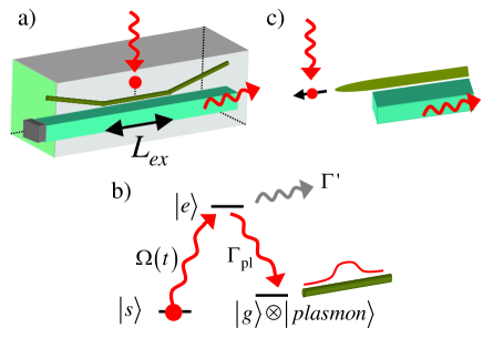
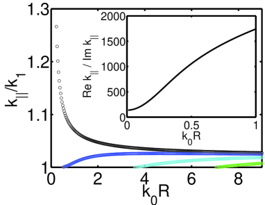
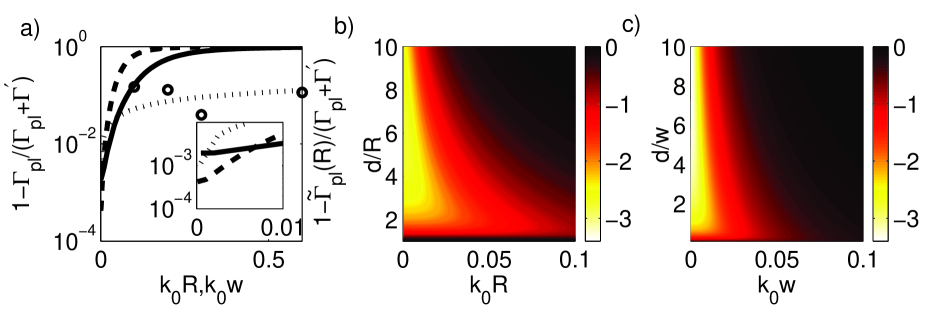
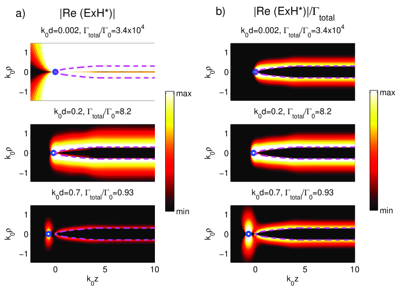
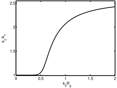
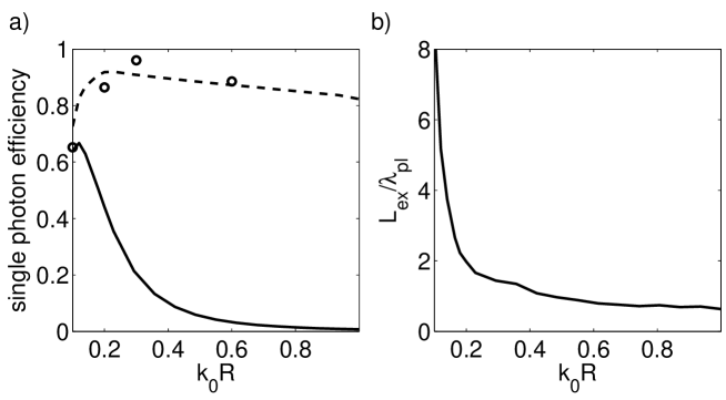
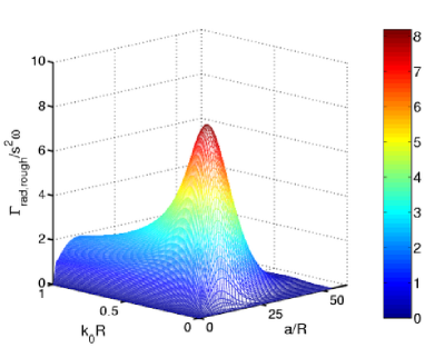
| Roughness parameters | ( nm) | ( nm) | ( nm) |
| , () | |||
| , () | 0.4% | 1.9% | 5.6% |
| , () | 0.9% | 4.5% | 12% |
| , () | 2.8% | 8.0% | 10% |
| , () | |||
| , () | 0.9% | 2.9% | 3.8% |
| , () | 0.3% | 1.3% | 1.8% |
| Roughness parameters | ||
|---|---|---|
| , () | 0.2% | 0.2% |
| , () | 7.5% | 6.8% |
| , () | 0.03% | 1.0% |
| , () | 0.9% | 26% |
| , () | 3.5% | 110% |
| , () | 2.7% | |
| , () | 0.2% | 67% |
| , () | 0.8% | 270% |