Electron impact ionization loading of a surface electrode ion trap
Abstract
We demonstrate a method for loading surface electrode ion traps by electron impact ionization. The method relies on the property of surface electrode geometries that the trap depth can be increased at the cost of more micromotion. By introducing a buffer gas, we can counteract the rf heating assocated with the micromotion and benefit from the larger trap depth. After an initial loading of the trap, standard compensation techniques can be used to cancel the stray fields resulting from charged dielectric and allow for the loading of the trap at ultra-high vacuum.
Surface electrode ion traps Chiaverini et al. (2005); Pearson et al. (2006); Seidelin et al. (2006); Britton et al. (2006) offer significant potential for realizing complicated geometries needed for large-scale quantum computation Kielpinski et al. (2002). Their advantages include greater ease of fabrication than three dimensional (3D) layered planar traps Barrett et al. (2004); Madsen et al. (2004); Stick et al. (2006) and the ability to integrate control electronics below the electrode surface Kim et al. (2005). However, the 2D geometery results in a shallow trap depth, which is of comparably sized 3D traps Chiaverini et al. (2005). In the presence of stray electric fields, the depth can become even shallower.
Stray electric fields can also displace ions from the zero point of the trap radiofrequency (rf) field. This causes undesired heating of ions, resulting from coupling of the rf-driven “micromotion” of one ion with the secular motion of neighboring ions. A well-developed technique to mitigate this effect is to apply dc compensation voltages, usually to special electrodes placed around the ion Berkeland et al. (1998); Raab et al. (2000); Lisowski et al. (2005).
To find the experimental dc compensation values, one typically starts with the compensation values for an ideal trap. For a symmetric 3D linear trap, the expected compensation values are zero. The asymmetry of the 2D linear trap requires numerically solving Maxwell’s equations to find compensated dc electrode values Seidelin et al. (2006) since the dc voltages used to confine the ions axially also shift the ion positions vertically, and since dielectric insulators needed between electrodes are neglected in analytical solutions. If an ion signal is easily observed, the experimental compensated values can be quickly found. However, large stray fields or trap imperfections often impede observation of ion signal and a random walk of the compensation voltages must be undertaken.
Electron impact ionization, the standard method for loading ion traps, charges dielectrics in the vacuum chamber, leading to large stray fields. Photoionization can be used to avoid creating stray charge at the cost of additional lasers and has been used to load shallow 2D and 3D traps Seidelin et al. (2006); Stick et al. (2006). Here we demonstrate a method for loading 2D traps with electron impact ionization that relies on the asymmetry of the trap and a buffer gas to obtain the initial signal.
An uncompensated trap leads to an increase in micromotion and is never advantageous for a 3D geometry. However, for a 2D geometry an applied field perpendicular to the surface can result in a significantly deeper trap in exchange for more micromotion Pearson et al. (2006). In this setting, the number of ions loaded increases but laser cooling is not efficient enough to counter the rf heating, causing the ions to escape.
The increase in rf heating can be counteracted by introducing a non-reactive buffer gas Dehmelt (1969); Moriwaki (1992) that reduces ion temperature through collisional damping of hot ion motion. The buffer gas allows us to initially load the trap and determine the value of stray fields. After the stray fields have been compensated, the trap can be loaded at ultra-high vacuum (UHV).
We demonstrate this loading method using strontium ions in a mm-scale surface electrode trap. Following the design of a traditional four-rod linear Paul trap system Berkeland (2002), the trap is mounted in a standard UHV chamber pumped down to torr, loaded with by electron impact ionization of neutral atoms from a resistive oven source, and driven by an externally mounted helical resonator. An optional, controlled buffer gas environment of up to torr of ultra-pure helium is provided though a sensitive leak valve, monitored with a Bayard-Alpert ion gauge.
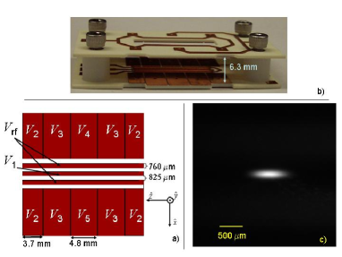
Our surface electrode ion trap has five electrodes Chiaverini et al. (2005); Pearson et al. (2006): one center electrode at ground, two at rf potential, and two segmented dc electrodes (Fig. 1). The electrodes are copper, deposited on a low rf loss substrate (Rogers 4350B), and fabricated by Hughes Circuits following standard methods for microwave circuits. In the loading region, slots are milled between the rf and dc electrodes to prevent shorting due to strontium buildup. The inner surfaces are plated with copper to minimize trap potential distortion due to accumulation of stray surface charges. The trap surface is polished to a m finish to reduce laser scatter into the detector.
Ions are detected by laser induced fluorescence of the main nm transition of strontium Berkeland (2002), using either an electron-multiplying CCD camera (Princeton Instruments PhotonMax) or a photomultiplier tube (Hamamatsu H6780-04). A laser tuned to nm addresses the transition to prevent shelving from the state to the metastable state. The two external cavity laser diode sources are optically locked to low finesse cavities Hayasaka (2002). Typical laser powers at the trap center are mW at nm and - W at nm.
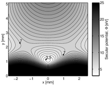
The first step for loading a surface electrode trap is determination of the ideal compensation voltages needed to offset the inherent asymmetry. We determine these potentials numerically (using CPO, a boundary element electrostatic solver Brkić et al. (2006)), by computing the rf and dc potentials ( and ), which give the secular potential where is the ion mass and is the ion charge. Typically, is of - V amplitude at MHz, and dc electrode voltages (as defined in Fig. 1) are V, V, and V. Shown in Fig. 2 is a cross-section of the secular potential in the - plane, at , for three different values of . As demonstrated in Fig. 3, with these voltages and V applied to the top electrode, the trap should be compensated with a trap depth of eV. The trap depth can be increased to eV by setting V, at the cost of increased micromotion.
a) b)
![[Uncaptioned image]](/html/quant-ph/0603142/assets/x2.png)
c)
![[Uncaptioned image]](/html/quant-ph/0603142/assets/x4.png)

These ideal compensation voltages often differ substantially from actual ones, due to the presence of unknown stray charges in the trap. A variety of techniques have been developed to experimentally determine the appropriate voltages, including examination of the single ion spectrum Raab et al. (2000); Lisowski et al. (2005), the correlation between ion fluorescence and the rf drive phase Berkeland et al. (1998), and the change in ion position with pseudopotential depth Berkeland et al. (1998). The first two methods require cold and small ion clouds necessitating good initial compensation. We use the last method, which is also applicable to large hot ion clouds.
We employ buffer gas cooling to load and maintain the large ion clouds needed for experimental determination of appropriate compensation voltages. Initially, when the cloud center is 0.2 mm from the rf node, the size and lifetime of the loaded cloud depends strongly on the buffer gas pressure (Fig. 4). Notably, lifetimes at UHV were too short to be measured in the uncompensated trap. Based on the data in Fig. 4, we perform our compensation experiments at torr. This pressure yields an excellent signal to noise ratio ( for a ms integration time with the photomultiplier tube) and long ion lifetime ( s) without overburdening the ion pump.
An accurate value of the stray dc field can be calculated from the cloud motion using the following model. The electric field along a coordinate , at the rf node, is well approximated by . For an rf pseudopotential with secular frequency , the ion motion follows , which results in a new secular frequency , and a new cloud center position . By measuring both the secular frequency and the ion center, one can determine .
We experimentally determine by measuring the cloud center position as a function of applied voltages. The nm laser is configured to illuminate the entire trapping region, while the nm laser is focused to a m spot; the focal point is translated in the - plane by using a precision motorized stage. Ion cloud fluorescence intensity, measured by the PMT, is recorded as a function of laser position, and fit to a Gaussian centered at the ion cloud position Siemers et al. (1988). This measurement is then repeated at different rf voltages, and a linear fit of the cloud center positions to determines the stray dc field value . is determined by applying an oscillating voltage on of 250 mV and observing dips in the ion fluorescence.

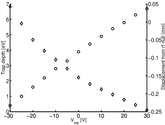
The data obtained, shown in Fig. 5, give an excellent match of the cloud intensity to a Gaussian fit, allowing measurement of the cloud center to within m. Thus, the measurement of stray fields is precise to about V/m at zero stray field. From the stray field measurements, we determine the required compensation voltages to be V and V. The estimated residual displacement of a single ion at these voltages is less than m. The nonlinear dependence of the dc electric field along on the top electrode voltage is due to the strong anharmonicity of the trap in the vertical direction, unaccounted for in the simple linear model employed in the analysis.
The difference between measured and ideal compensation voltages is evidence of anisotropic stray fields, caused by undetermined surface charges. The estimated stray fields along are comparable to those reported for 3D traps Berkeland et al. (1998). However, the stray fields along are times larger. The V difference between the calculated and measured values of at compensation suggests significant electron charging on either the trap surface, the top plate, or the top observation window.
In summary, we have loaded a surface electrode ion trap by electron impact ionization at UHV by using an uncompensated trap to increase trap depth and a large cloud in buffer gas to find the compensation values. The results suggest that the open geometry of the trap makes it more susceptible to stray surface charges. The technique demonstrated will likely be useful for the loading of complex and integrated surface electrode ion traps.
Support for this project was provided in part by the JST/CREST Urabe Project, and MURI project F49620-03-1-0420. We thank Rainer Blatt, Richart Slusher, Vladan Vuletic, and David Wineland for helpful discussions.
References
- Chiaverini et al. (2005) J. Chiaverini, R. B. Blakestad, J. Britton, J. D. Jost, C. Langer, D. Leibfried, R. Ozeri, and D. J. Wineland, Quant. Inf. and Comp. 5, 419 (2005).
- Pearson et al. (2006) C. E. Pearson, D. R. Leibrandt, W. S. Bakr, W. J. Mallard, K. R. Brown, and I. L. Chuang, Phys. Rev. A 73, 032307 (2006).
- Seidelin et al. (2006) S. Seidelin, J. Chiaverini, R. Reichle, J. J. Bollinger, D. Leibfried, J. Britton, J. H. Wesenberg, R. B. Blakestad, R. J. Epstein, D. B. Hume, J. D. Jost, C. Langer, R. Ozeri, and D. J. Wineland, quant-ph/0601173.
- Britton et al. (2006) J. Britton, D. Leibfried, J. Beall, R. B. Blakestad, J. J. Bollinger, J. Chiaverini, J. H. Wesenberg, R. J. Epstein, J. D. Jost, D. Kielpinski, C. Langer, R. Ozeri, S. Seidelin, R. J. Reichle, N. Shiga, J. H. Wesenberg, and D. J. Wineland, quant-ph/0605170.
- Kielpinski et al. (2002) D. Kielpinski, C. Monroe, and D. J. Wineland, Nature 417, 709 (2002).
- Barrett et al. (2004) M. D. Barrett, J. Chiaverini, T. Schaetz, J. Britton, W. M. Itano, J. D. Jost, E. Knill, D. Leibfried, C. Langer, R. Ozeri, and D. J. Wineland, Nature 429, 737 (2004)
- Madsen et al. (2004) M. J. Madsen, W. K. Hensinger, D. Stick, J. A. Rabchuk, and C. Monroe, Appl. Phys. B 78, 639 (2004).
- Stick et al. (2006) D. Stick, W. K. Hensinger, S. Olmschenk, M. J. Madsen, K. Schwab, and C. Monroe, Nature Physics 2, 36 (2006).
- Kim et al. (2005) J. Kim, S. Pau, Z. Ma, H. R. McLellan, J. V. Gates, A. Kornblit, R. E. Slusher, R. M. Jopson, I. Kang, and M. Dinu, Quant. Inf. Comp. 5, 515 (2005).
- Berkeland et al. (1998) D. J. Berkeland, J. D. Miller, J. C. Bergquist, W. M. Itano, and D. J. Wineland, J. Appl. Phys. 83, 5025 (1998).
- Raab et al. (2000) C. Raab, J. Eschner, J. Bolle, H. Oberst, F. Schmidt-Kaler, and R. Blatt, Phys. Rev. Lett. 85, 538 (2000).
- Lisowski et al. (2005) C. Lisowski, M. Knoop, C. Champenois, G. Hagel, M. Vedel, and F. Vedel, Appl. Phys. B 81, 5 (2005).
- Dehmelt (1969) H. G. Dehmelt, Adv. At. Mol. Phys. 5, 109 (1969).
- Moriwaki (1992) Y. Moriwaki, M. Tachikawa, Y. Maeno, and T. Shimizu, Jpn. J. Appl. Phys 31, L1640 (1992).
- Berkeland (2002) D. J. Berkeland, Rev. Sci. Inst 73, 2856 (2002).
- Hayasaka (2002) K. Hayasaka, Opt. Comm. 206, 401 (2002).
- Brkić et al. (2006) B. Brkić, S. Taylor, J. F. Ralph, and N. France, Phys. Rev. A 73, 012326 (2006).
- Siemers et al. (1988) I. Siemers, R. Blatt, T. Sauter, and W. Neuhauser, Phys. Rev. A 38, 5121 (1988).