Experimental test for the conductivity properties from the Casimir force between metal and semiconductor
Abstract
The experimental investigation of the Casimir force between a large metallized sphere and semiconductor plate is performed using an atomic force microscope. Improved calibration and measurement procedures permitted reduction in the role of different uncertainties. Rigorous statistical procedures are applied for the analysis of random, systematic and total experimental errors at 95% confidence. The theoretical Casimir force is computed for semiconductor plates with different conductivity properties taking into account all theoretical uncertainties discussed in literature. The comparison between experiment and theory is done at both 95 and 70% confidence. It is demonstrated that the theoretical results computed for the semiconductor plate used in experiment are consistent with data. At the same time, theory describing a dielectric plate is excluded by experiment at 70% confidence. Thus, the Casimir force is proved to be sensitive to the conductivity properties of semiconductors.
pacs:
12.20.Fv, 12.20.Ds, 68.37.PsI Introduction
The Casimir force 1 is a phenomenon originating from quantum fluctuations. It depends on both the Planck constant and the velocity of light . At the shortest separations of a few nanometers the relativistic effects become negligible and quantum fluctuations give rise to the familiar van der Waals force. The experimental interest in the Casimir effect (see Refs. 2 ; 3 ; 4 ; 5 ; 6 ; 7 ; 8 ; 9 ; 10 ; 11 ; 12 and review 13 ) is motivated by the important role played by fluctuating phenomena in different fields of physics. One of the most important applications of the Casimir force is in nanotechnology. Microdevices and microstructures are fabricated from semiconductors and their characteristic sizes are of micrometers to nanometers, i.e., distance scales where the Casimir and van der Waals forces become dominant 8 ; 13 ; 14 ; 15 . Another notable application of precision experiments is in the search for new fundamental interactions and hypothetical particles where the Casimir force makes the largest contribution to the background 11 ; 12 ; 13 ; 16 ; 17 ; 18 ; 19 .
All experiments in Refs. 2 ; 3 ; 4 ; 5 ; 6 ; 7 ; 8 ; 9 ; 10 ; 11 ; 12 deal with metallic test bodies. However, the most important materials used in nanotechnology are semiconductors with conductivity properties ranging from metallic to dielectric. Measuring the van der Waals and Casimir forces between dielectrics has always been a problem due to the need to eliminate residual charges and contact potential differences 13 . Semiconductors with a relatively high conductivity have an advantage that they avoid accumulation of residual charges but, at the same time, possess a typical dielectric dependence of the dielectric permittivity on frequency within a wide frequency range. This makes it possible to examine the influence of material properties on the Casimir force and opens new opportunities to modulate the magnitude and separation dependence of the force by using semiconductors of different conductivity. We should note that an early attempt to measure the van der Waals force in semiconductor surfaces and modify them by light was reported in Ref. 19a . The force was measured between a glass lens and Si plate and also between the glass lens coated with Si in a small region and the same Si plate. As the glass lens is an insulator, the forces due to work function potential differences could not be controlled. This might explain why no force change occured on illumination for small separations below 350 nm 19a where it should have been most pronounced, given the approximate inverse third power distance dependence of the Casimir force for this geometry.
Recent Ref. 20 presents the first measurement of the Casimir force between a large gold coated sphere and single crystal silicon plate with a resistivity cm. The obtained experimental results were compared with the Lifshitz theory at zero temperature and excellent agreement was obtained. It was shown that the Casimir force between Au-Si bodies decreases with the increase of separation distance more quickly than between Au-Au bodies. In Ref. 20 the conclusion was made that this behavior of a metal-semiconductor system in comparison with the case of two metals can be used to control the Casimir force in micro- and nanoelectromechanical systems. An additional interest in the case of dissimilar materials of the Casimir plates (metal and dielectric) was stimulated by new theoretical results. As was shown in Ref. 21 , the Casimir pressure and the free energy of a fluctuating field between metal and dielectric are nonmonotonous functions of temperature in some temperature intervals. This leads to the possibility of the negative Casimir entropy although it always vanishes when the temperature goes to zero (i.e., the Nernst heat theorem is satisfied).
In this paper we continue the experimental investigation of the Casimir force between an Au sphere and a Si plate using the experimental setup described in Ref. 20 . We apply the improved procedures in sample preparation and in calibration of the setup. This reduces the role of different uncertainties and leads to important new results concerning the influence of semiconductor conductivity on the Casimir force. The analysis of the obtained experimental data is performed at 95% confidence, and random, systematic and total experimental errors are determined using rigorous methods of mathematical statistics. In particular, the experimental data are analyzed for the presence of outlying results. The surface roughness on both the Si plate and the Au coated sphere is investigated using an atomic force microscope. This experiment (performed at K) is shown to be insensitive to the temperature corrections predicted by different approaches to the thermal Casimir force (see, e.g., Refs. 22 ; 23 ). Because of this, the experimental data are compared with the Lifshitz theory at zero temperature using the tabulated optical data for the complex refractive indices of Au and Si 24 . Different kinds of theoretical errors and corrections (in particular, the correction due to surface roughness) are calculated or estimated. The resulting total theoretical error is found at 95% confidence. The comparison between experiment and theory is performed at both 95% and 70% confidence using a rigorous statistical approach. The theoretical results computed for the p-type B doped Si plate of resistivity cm used in the experiment are found to be consistent with the experimental data. At the same time, the theoretical results computed for high resistivity (“dielectric”) Si with cm (as in tables of Ref.24 ) are excluded experimentally at 70% confidence. Hence our experiment demonstrates how the Casimir force between a metal and a semiconductor is influenced by the conductivity properties of the latter. Changing the density of free carriers inside a semiconductor by means of doping or irradiation with light will lead to changes in the Casimir force.
The paper is organized as follows. In Sec. II we briefly describe the experimental setup, and the sample preparation and characterization including the determination of surface roughness profiles. Sec. III describes the measurement of the deflection coefficient, determination of the residual electrostatic force and separation on contact, and calibration. Sec. IV contains the measurement results for the Casimir force and the statistical analysis of the experimental errors. In Sec. V the theoretical results for the Casimir force between a metal and semiconductor in the experimental configuration are presented, and the theoretical errors are estimated. In Sec. VI the comparison between experimental data and theoretical results computed for Si samples of different resistivity is performed. Sec. VII contains our conclusions and discussion.
II Experimental setup, and sample preparation and characterization
To measure the Casimir force between an Au coated sphere and a single crystal Si plate, we have used an improved setup over that in Ref.6 for both test bodies coated by Au. In the present experiment the sphere was coated with an Au layer of 105 nm thickness and had a diameter m. It was attached to the cantilever of an atomic force microscope. In the atomic force microscopy technique the force is measured through a deflection of the cantilever attached to the sphere. The Si plate (doped with B) had an area and thickness of 350 m. The resistivity of the plate cm was measured using the four-probe technique. Note that the resistivities of metals are usually two or three orders of magnitude lower. Because of this, our Si plate has a relatively large absorption typical of semiconductors for all frequencies contributing to the Casimir force at experimental separations.
The main improvements in experimental setup in comparison with Ref.6 are the use of much higher vacuum, and the reduction of the uncertainty in the determination of absolute sepatations . A much higher vacuum (Torr instead of Torr in Ref.6 ) is needed to maintain the chemical purity of the Si surface which otherwise oxidizes rapidly to SiO2. The high-vacuum system is needed to prevent contamination. It consists of oil-free mechanical pumps, turbo pumps, and ion pumps. To maintain the lowest pressure during data acquisition, only the ion pump is used. This helps to reduce the influence of mechanical noise. The absolute error in the determination of absolute separations was reduced to nm in comparison with nm in Ref.6 . This was achieved by using a piezo capable of traveling a distance of 6 m from initial separation to contact of the test bodies (in Ref.6 piezo movement was used only at separations less than 2 m, and the movement to larger separations of the plate from the sphere was done mechanically). Such large piezo extensions were also found necessary to allow time for the decay of noise associated with the separation of the gold sphere and plate after contact of the two surfaces. The complete movement of the piezo, , was calibrated using a fiber optic interferometer 24a . To extend and contract the piezo, continuous triangular voltages at 0.02 Hz are applied to the piezo. Given that the experiment is done at room temperature, applying of static voltages will lead to piezo creep and loss of position sensitivity. The extension and contraction of the piezo were fit to terms up to fourth order in the applied voltage. Because of this, the error in piezo calibration practically does not contribute to .
As opposed to Au, the Si surface is very reactive. Because of this, a special passivation procedure is needed to prepare it to force measurements. For this purpose nanostrip (a combination of H2O2 and H2SO4) is used to clean the surface of organics and other contaminants. This cleaning, however, oxidizes the surface. Then 49% HF solution was used to etch SiO2. This procedure also leads to hydrogen termination of the surface. The hydrogen termination prevents the re-oxidation of Si surface as long as it is kept in a high vacuum environment. The termination is stable for more than two weeks under the vacuum conditions described above 26 ; 27 . We have checked the effectiveness of the passivation technique to prevent the contamination of the Si surface through the measurement of the distance dependence of the electrostatic force resulting from the residual potential difference between the interacting surfaces (see Sec. III).
To characterize the topographies of both samples, the Au coating of the sphere and the surface of Si plate were investigated using an atomic force microscope. Images resulting from the surface scan of Au coating demonstrate that the roughness is mostly represented by the stochastically distributed distortions of about 8–22 nm. In Table I the fractions of the Au coating with heights () are presented in columns 3 and 2, respectively. The surface scan of Si surface shows much smoother distortions with the typical heights from 0.4 to 0.6 nm and with a maximal height equal to only 1 nm. The fractions of the Si surface with heights () are presented in columns 3 and 2 of Table II, respectively. Data in Tables I and II are used in Sec. V to compute the correction to the theoretical Casimir force due to surface roughness.
III Calibration of the setup and determination of the residual electrostatic force and separation on contact
All calibrations and determination of the residual electrostatic force and of the separation on contact are done immediately before the Casimir force measurements in the same high vacuum apparatus. As was already mentioned in Sec. II, the force is determined through a deflection of the cantilever. The calibration of the deflection signal, , which is negative for attractive force and is measured by using two photodiodes either as a current or a voltage, is done by applying dc voltages to the Si plate. Care was taken to make ohmic electrical contacts to the silicon. Direct contact to the Si plate leads to large residual potentials. Because of this, the electrical contact was made from a 100 nm thick gold pad attached to the bottom of the plate. The electrical contact to the gold sphere was accomplished by applying a very thin gold coating to the cantilever. In addition, a small correction has to be applied to the separation distance between the gold sphere and the Si plate due to the movement of the cantilever. The actual separation distance between the bottom of the gold sphere and the Si plate is given by
| (1) |
where is the deflection coefficient in units of nm per unit deflection signal.
The measurement of was performed by applying different dc voltages between to V to the plate. To find the coefficient , the cantilever deflection signal was measured as a function of the distance. The 0.02 Hz triangular wave was applied to the piezo to change the distance between the sphere and the plate. Larger applied voltages lead to more cantilever deflection and therefore earlier contact of the two surfaces. The change in the contact position of the sphere and the plate as a function of the applied voltage can then be used to measure deflection coefficient 6 . In order to determine the contact of the two surfaces precisely, 32768 data points at equal time intervals were acquired for each force measurement. In distinction to Ref. 6 , in cases, where the contact was between two neighboring data points, a linear interpolation was used to identify the exact value. The deflection coefficient was found to be nm per unit deflection signal. This value was used to correct the separation distance in all measurements.
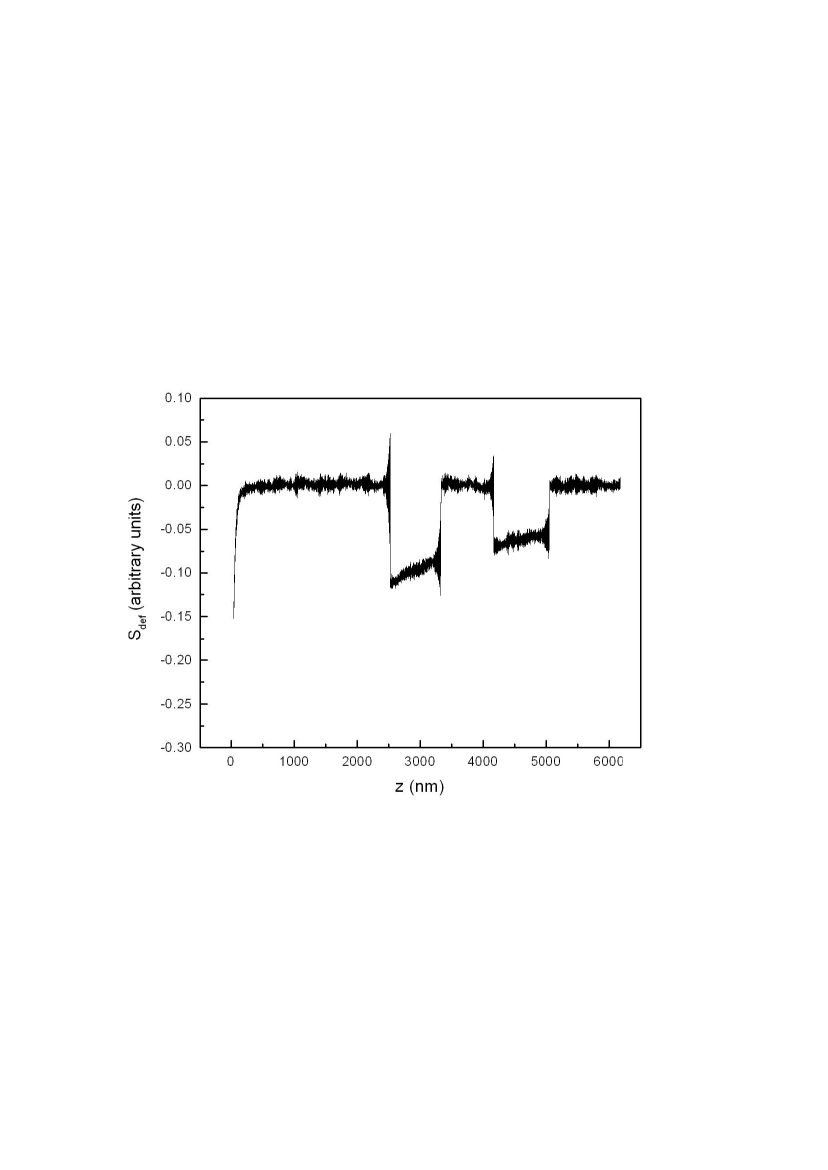
The determination of the residual potential difference between the two surfaces was performed by the fit between electric force measurements far away from contact (where the Casimir force is practically zero) and exact force-distance relation. To measure the force, the calibration of the deflection signal was performed. In this work an improved method, rather than simple application of a dc voltage to the plate, was used. This was done to avoid systematic errors due to scattered laser light. In addition to the application of the dc voltage to the Si plate, square voltage pulses of amplitudes in the range V and time interval corresponding to a separation distance between 1 to 5 m were also applied to the plate. The dc voltage was close to the residual potential difference in order to decrease systematic errors due to large deflections. Fig. 1 shows the deflection signal of the cantilever in response to both the applied dc voltage and the square pulse as a function of the separation distance between the gold sphere and Si plate. By measuring only the difference in signal during the pulse allows one to avoid the need for a background subtraction. Also the large width of the pulse allowed checks for the distance dependence of the residual potential and any position dependence in the calibration.
The average values of the measured electric forces as a function of separation were used to fit the exact force-distance relation 25
| (2) |
where , is the voltage applied to the Si plate, and is a permittivity of a vacuum. Nonzero value of at contact, , is due to surface roughness. This is a distance between the zero roughness levels [see Eq. (26) below]. For application to this experiment, Eq. (2) is conveniently rearranged as follows
| (3) |
where
Within the separation region from 1.8 to 5 m, the relative error introduced by the use of Eq. (3) instead of Eq. (2) does not exceed . Eq. (3) at fixed separation is used to fit the difference signal and the residual potential difference was determined to be V. The calibration of the deflection signal was also performed using the same procedure. The force calibration constant was determined to be nN per unit cantilever deflection signal.
The value of was found to be independent of separation. This confirms the absence of localized charges because they would lead to dipole and other multipolar electrostatic fields, resulting in a residual potential difference varying with distance. As was mentioned above, the relatively high conductivity of the Si plate, used in this experiment, is important in preventing the formation of the localized charges. The independence of on separation confirms also the absence of any contamination of the Si surface.
The separation distance on contact of the two surfaces needs to be independently determined for a comparison of the measured Casimir force to the theory. To achieve this goal, we apply different dc voltages to the Si plate (like it was done in the measurement of ) and measure the electrostatic force as a function of separation. This measurement at each voltage was repeated 5 times and the average signal curve was obtained. A compensation dc voltage equal to was applied to the plate and the resulting deflection signal was subtracted from the signal corresponding to electrostatic force curves at all other dc voltages. This procedure eliminates the need for subtraction of the background and Casimir forces from the electrostatic force curves. In difference from Ref. 6 , in the determination of we attempted to reduce the role of uncertainties in . The procedure used here also gives one more way for the determination of and check of its distance independence. It is as follows: At a fixed separation different voltages are applied to the plate and the electrostatic force is plotted as a function of . The parabolic dependence of this force [see Eq. (3)] is used to determine the values of and Overbeek . This is repeated for many different . The value of was found to be the same as that determined earlier and to be independent on separation distance. Note that this determination is also independent of errors in the cantilever calibration. In order to determine , is then plotted as a function of and fitted to Eq. (3). The value of so determined is 32.1 nm. The uncertainty in the quantity [see Eq. (1)] due to both the uncertainty in and calibration was found to be 0.8 nm. As was mentioned in Sec. II, the error in piezo calibration contributes negligibly to the error in measurement of absolute separations . Because of this, with account of Eq. (1), we arrive at nm. (Note that in Ref. 20 for the sake of brevity the uncertainty in was attributed to .)
IV Measurement results and experimental errors
The Casimir force between the sphere and the plate was measured as a function of distance. In doing so the sphere was kept grounded while a compensating voltage was applied to the plate to cancel the residual electrostatic force. The distance was varied continuously from large to short separations by applying continuous triangular voltages at 0.02 Hz to the piezo. The piezo was extended to its maximum range over 6 m. The force data were collected at 32768 equal time intervals as the distance between the sphere and plate was changed. This measurement was repeated for times. A great advantage of the atomic force microscopy technique in the averaging is that the contact point between the two surfaces provides a starting point for alignment of all the 65 measurements. Nevertheless, thermal noise in the cantilever deflection signal, , leads to noise in the corresponding separations . To account for this in the averaging, the separation distance is divided into a grid of 32768 equidistant points separated by 0.17 nm. For each measured Casimir force-distance curve, the value of the force at the grid point is computed using linear interpolation of the neighboring two data points. Because the separation distance between neighboring points is small as 0.17 nm, higher order interpolation procedures were not required. Also the noise spectrum and amplitude of the interpolated data were confirmed to be the same as the raw data. This allowed the averaging of the 65 Casimir force mesurements even including the effect of the change in the separation distance due to the thermal noise of a cantilever.
Below we present the measurement results within the separation range from 62.33 nm to 349.97 nm. This distance range (containing 1693 points) is chosen for the reason that for larger separations the experimental relative error of force measurements caused by the noise exceeds 100% (see below), i.e., the data are not informative. Data for separations below 62.33 nm up to contact are not presented as nonlinearities associated with the “jump to contact” introduce uncontrollable errors into the force measurement.
For convenience we denote the separations by , where and . In the present experiment the separations with fixed are the same in all measurement sets, i.e., do not depend on . The mean values of the force
| (4) |
are plotted in Fig. 2 as a function of separation within the chosen separation range. As is seen from Fig. 2, at short separations the mean force is uniform, i.e., changes smoothly with the change of . Several values of the mean experimental force are listed in column 2 of Table III.
Before proceeding with the analysis of random errors, we examine the experimental data for the presence of so-called “outlying” results. For this purpose it is necessary to consider the quantity 28 ; 29
| (5) |
where maximum is taken with respect to , and the variance of the force is
| (6) |
According to standard statistical procedure, the measurement set contains the outlying result at a point with a confidence probability if the inequality is satisfied, where are tabulated quantities 28 ; 29 . Usually the set of measurements is rejected if it contains results which are outlying at a confidence probability 90%. Using this statistical criterion we have analyzed all sets of measurements and found that changes from 2.4 to 2.7. For a bilateral check [which is applicable because in our case the deviations of from are both positive and negative] 28 ; 29 . Hence it follows that there are no outlying results among our measurement data and all of them should be used in the determination of the experimental errors.
We start with random errors and find the variance of the mean force
| (7) |
Direct calculation shows that the variance of the mean, , is not uniform, i.e., changes stochastically in going from one to another. The computational results for this variance as a function of separation are shown in Fig. 3. To smooth the variance of the mean, we have used a special procedure developed in mathematical statistics 30 ; 31 . For each separation we consider neighboring points (half of them from the left and half from the right of ; in this experiment). Then the smoothed variance of the mean force at a point is given by 30 ; 31
| (8) |
where are the statistical weights. The two different sets of the statistical weights can be chosen:
| (9) |
where constants are determined from
Here we choose in Eq. (8). This leads to larger values of and, thus, is a more conservative estimate, overestimating the random errors. In our experiment the application of this statistical procedure results in approximately the same variance for all equal to pN.
Now we are in a position to find the absolute random error for the Casimir force measurements in the configuration of Au sphere and Si plate. Using the Student’s -distribution with a number of degrees of freedom and choosing the 95% confidence probability (), we obtain and 32 . Thus, the absolute random error does not depend on separation and is given by
| (10) |
The relative random error is defined as
| (11) |
The values of the relative random error as a function of separation are given in the second column of Table IV. It achieves the smallest value equal to 0.78% at the shortest separation nm and increases with the increase of separation.
There are following four systematic errors in this experiment 20 : pN due to the error in force calibration; pN due to noise when the calibration voltage is applied to the cantilever; pN due to the instrumental sensitivity; and pN due to the restrictions on computer resolution of data. Systematic errors are random quantities characterized by a uniform distribution. The best estimate for their combination, i.e., for a total systematic error at a given confidence probability , is given by 28
| (12) |
where in our experiment , and is a tabulated coefficient. Using the value we obtain from Eq. (12) pN at 95% confidence. In the third column of Table IV the values of the relative systematic error
| (13) |
are listed at different separations. As is seen from this Table, the smallest relative systematic error of 0.31% is achieved at the shortest separation. Comparing second and third columns in Table IV, we conclude that at all separations the magnitude of the systematic error comprises about 0.4 of the random error.
To find the total experimental error in the Casimir force measurements, one should combine the random and systematic errors obtained above. They are described by a normal (or Student) distribution, and by a combination of uniform distributions, respectively. To be very conservative, we assume that the combination of systematic errors is also described by a uniform distribution (other assumptions would lead to a smaller total error). Different methods for combining random and systematic errors are described in literature 28 . Here we use the rule based on the consideration of the ratio
| (14) |
If the inequality is satisfied, the systematic error in most cases can be neglected and the total error at 95% confidence is given by
| (15) |
If , the random error can be neglected and the total error at the same confidence is
| (16) |
In the region where it is recommended 28 to use the expression
| (17) |
with a maximum possible value of the coefficient determined at 95% confidence. In our case the random error exceeds the systematic one, and the value of in Eq. (14) is constant and close to 0.8. Because of this, to be conservative, we choose the largest of the total errors given by Eqs. (15) and (17), i.e., pN.
In the fourth column of Table IV we present the values of the relative total experimental error
| (18) |
at different separations. It is equal to only 0.87% at the shortest separation and achieves 64% at a separation nm. At nm the total experimental error exceeds 100%. Comparing second, third and fourth columns in Table IV, one can conclude that at all separations the major contribution to the total experimental error is given by the random error.
V Theoretical approach to the Casimir force between metal and semiconductor
As was demonstrated in the preceeding section, the lowest total experimental errors ranging from 0.87 to 5.3% are achieved at separations nm. At such short separations the thermal effects are not important (see below for the magnitudes of predicted thermal corrections) and one can use the Lifshitz formula at zero temperature for the Casimir (van der Waals) force acting between a Si plate and an Au sphere
| (19) |
Here the reflection coefficients for two independent polarizations of the electromagnetic field are
| (20) |
where
| (21) |
is the dielectric permittivity of Au () and Si (), and is the magnitude of the wave vector projection on the Si plate. Note that in Eq. (19) we have replaced a 105 nm Au layer for an Au semispace. Using the Lifshitz formula for layered structures [13], it is easy to calculate the force error due to this replacement. At a typical separation of 100 nm it is only 0.0095%, thus justifying the use of the semispace.
The dielectric permittivities of Au and Si along the imaginary frequency axis are computed by means of the dispersion relation
| (22) |
where are calculated using the tabulated optical data for the complex index of refraction 24 . For Au the data for eV are available (rad/s). To obtain by Eq. (22) with sufficient precision one should extrapolate the tabulated data to the region of smaller frequencies. This is usually done (see, e.g., Ref. 33 ) with the help of the imaginary part of the Drude dielectric function
| (23) |
where eV, and eV are the plasma frequency and relaxation parameter of Au, respectively. The most precise computational results for using this procedure are presented in Ref. 33 .
For dielectric Si with a resistivity cm the tabulated data for the complex refractive index are available for eV 24 . Thus, there is no need for any extrapolation of data to smaller frequencies. The computational result for the dielectric permittivity of dielectric Si along the imaginary frequency axis, , was obtained in Ref. 33 . It is shown by the dashed line in Fig. 4. This line can be extended to zero frequency leading to the value of the static dielectric permittivity of Si . The values of can be used in precise computations of the Casimir and van der Waals interactions between the test bodies made of dielectric Si. Note that the use of the analytical approximation for , suggested in Ref. 34 , leads to about 10% error in the magnitudes of the Casimir force, and, thus, is not suitable for the comparison with precise measurements.
In our experiment, however, the Si plate of much lower resistivity cm than in tables is used. This resistivity corresponds to B doped Si. The plasma frequency for such Si is equal to
| (24) |
Here the doping concentration leads to a carrier density . This value of corresponding to the sample of resistivity cm was obtained from Fig. 2.18 in Ref. 34a . The optical effective mass for B doped Si used in this experiment is 34b . The respective relaxation parameter of the Drude model is determined from rad/s. Since the optical properties of Si at the frequencies making a nonnegligible contribution to the Casimir force depend on the concentration of charge carriers, the optical data of dielectric Si should be adapted for our case. This is achieved 24 by adding the imaginary part of the Drude dielectric function to the imaginary part of the dielectric permittivity obtained from tables. For our Si plate of lower resistivity this results in
| (25) |
In Fig. 4 the dependence of on frequency is shown by the solid line. Once the dielectric permittivities of Au and Si along the imaginary frequency axis have been computed, the Casimir force can be found by Eqs. (19)–(21).
For comparison of theory with experiment, the theoretical results obtained using the Lifshitz formula should be corrected for the presence of surface roughness 6 ; 13 . The topography data in Tables I and II of Sec. II allow one to determine the zero roughness levels relative to which the mean values of the functions, describing roughness, are zero:
| (26) |
Calculations using Tables I and II lead to nm, nm. As was mentioned in Sec. III, all absolute separations between the test bodies are measured between the zero roughness levels determined in Eq. (26). This permits one to achieve rather low absolute error in separation measurements (nm in this experiment) in spite of the fact that the roughness heights are much larger (at least on the sphere).
In the framework of the additive approach 13 the Casimir force corrected for the presence of roughness can be calculated as
| (27) |
where is given by the Lifshitz formula (19). In this experiment the influence of surface roughness is very moderate. For example, if separation increases from 62.33 to 100.07 nm, the ratio computed using Eqs. (19) and (27) decreases from 1.015 to 1.006. Thus, the contribution of surface roughness achieves the maximum value of 1.5% at the shortest separation and decreases to only 0.6% at nm. Note that Eq. (27) takes into account the nonmultiplicative effects in corrections due to surface roughness and to realistic conductivity properties. A more simple multiplicative approach describes the surface roughness by the stochastic functions and presents the theoretical force in the form 13
| (28) |
where the variances of the random processes describing the stochastic roughness are given by
| (29) |
Calculations using Eq. (28) show that the ratio changes from 1.019 to 1.007 when separation increases from 62.33 to 100.07 nm. Thus, the maximal error of the multiplication approach in comparison with Eq. (27) is only 0.4%. At nm the error of the multiplication approach decreases to 0.1% of the force.
It is well known that the additive approach is the approximative one, and there are corrections to Eq. (27) due to the diffraction-type and correlation effects 35 ; 36 . For the case of Au-Au test bodies these corrections were estimated in Ref. 6 using the results of Ref. 35 . In our case of Au and Si test bodies the upper limit for the ratio computed within the multiplicative approach with account of the contribution of diffraction and correlation effects is 1.0204 at the shortest separation. This should be compared with 1.019 (where these effects were neglected) leading to only 0.14% difference. It is easily seen that the contribution of diffraction and correlation effects remains negligible over the separation range where the present experiment achieves high precision. At larger separations, however, where the contribution of these effects in the roughness correction increases, the complete roughness correction becomes negligible and the precision of the measurement decreases (see the second paper in Ref. [6] for more details).
Now we discuss the theoretical errors which may occur in the computation of the Casimir force using Eqs. (19) and (27). The first error arises from the variations of the tabulated optical data for the complex index of refraction for both Au and dielectric Si (recall that we have taken these data from tables in Ref. 24 ). As was shown in Ref. 6 , this error is no larger than 0.5%. Being conservative, we set % at all separations. In addition the tabulated optical data of the dielectric Si has to be modified due to the use of B doped Si according to Eq. (25). Note that the calculation results for the Casimir force are rather stable to the change of the Drude model parameters. Thus, a change of even by a factor of 1.5 leads to less than a 1% change in the Casimir force within the separation region from 62 to 150 nm. There may occur rare Au samples of bad quality leading to up to 2% deviations in the Casimir force at short separations in comparison with that computed using the tables. If such sample were used in the experiment, the theoretical Casimir force would deviate from the experimental data. Such deviations of the theory from experiment must be considered not as an error (note that they can only diminish the magnitude of the Casimir force) but as a correction similar to the roughness correction. The verification of the hypothesis of the presence of such types of corrections can be easily performed with the help of standard statistical procedures.
A second theoretical error is caused by the use of the proximity force theorem in Eq. (19). The exact value for the Casimir force in the configuration of a sphere above a plate is still unknown. Its magnitude may be both smaller or larger with equal probability than the estimate given by the proximity force theorem. The upper limit of the error introduced by the use of the proximity force theorem was estimated as 37 ; 38 .
Both errors and are described by a uniform distribution and, thus, are analogous to systematic errors. They can be combined by using Eq. (12) with , which is applicable to both absolute and relative errors. The values of the obtained theoretical error, , are presented in the fifth column of Table IV at different separations. This combined error slowly increases with the increase of separation and takes values between 0.55 and 0.64%.
In addition to the theoretical errors and discussed above, there exist the uncertainties due to patch potentials, nonlocal effects and that due to finite size of the plate which are not taken into account in Eqs. (19) and (27). All these uncertainties are shown to be negligibly small 6 ; 12 , and, thus, are neglected in the calculation of theoretical errors.
There is one more effect which is not taken into account in full in Eq. (19) but merits consideration. The measurements were performed at K. However, Eq. (19) is written in the form of an integral over the imaginary frequency which is related to zero temperature. The problem of the thermal Casimir force between conducting materials has been a matter of debate over the last few years and two different approaches to its resolution were suggested (see, e.g., Refs. 22 ; 23 ). According to Ref. 22 , the thermal corrections at short separations are negligibly small for any conducting materials in qualitative agreement with the case of ideal metals 13 . On the contrary, Ref. 23 predicts thermal correction which can be several hundreds times greater than that for ideal metals at short separations. In our experiment, however, even the large thermal correction predicted in Ref. 23 is negligibly small. For example, for Au sphere and Si plate of resistivity at nm the approach of Ref. 23 leads to the thermal correction equal to 0.015% of the zero-temperature force. This correction increases up to 0.039% at nm and to 0.13% at nm. With increasing separation, however, the precision of the measurements decreases more rapidly, so that the predicted thermal correction remains negligible. For Au sphere above a plate made of dielectric Si, the thermal correction is even smaller. Thus, at nm it is equal to only 0.005% of the zero-temperature force. It should also be noted that the optical properties of the materials are determined not at zero but at room temperature. Because of this, even the Lifshitz formula (19) includes some dependence of temperature as a parameter. Thus the use of the Lifshitz formula at zero temperature for the comparison with experimental data is well justified.
In the foregoing we did not discuss one more error which is in fact not theoretical but plays some role in the comparison of theory with experiment. This arises from the fact that the theoretical force should be calculated in the experimental points which are determined with an error 39 . Bearing in mind that the leading theoretical dependence has the form , this leads to the error ) determined at 95% confidence. The values of at different separations are presented in column 6 of Table IV. It is seen that at shortest separation %, i.e., much larger than the proper theoretical error . At nm %, i.e., also larger than . In a conservative way the errors and can be combined using the analogues of Eqs. (16) and (17) written in terms of relative errors. Thus, we obtain what we call the total theoretical error at 95% confidence presented in column 7 of Table IV as a function of separation. Comparing column 7 with column 5, we conclude that the error in the theoretical forces due to uncertainties in experimental separations is in fact the most important factor in the determination of the total theoretical error at short separations. This concludes the analysis of the theoretical errors.
Using Eqs. (19) and (27), the Casimir forces were computed at all experimental points for the sample of resistivity used in experiment. A few results at different separations are presented in column 3 of Table III. Column 5 of Table III contains typical differences at different . The same computation was repeated for dielectric Si resulting in Casimir forces presented in column 4 of Table III. The typical differences are listed in column 7 of the same table. The comparison of both sets of theoretical computations with experiment using a rigorous statistical approach is performed in the next section.
VI Comparison of experiment and theory as a test for conductivity properties
To compare experiment with theory, we consider the random quantity , where is a stochastic function with a mean . In fact, in Sec. V we have discussed the uncertainties of just this stochastic function and not of the usual function computed by the Lifshitz formula (19) and corrected for the presence of roughness in Eq. (27). Thus, it is implied that . The absolute error of at 95% confidence is denoted by . It can be found using the composition rule (12) with and :
| (30) |
Note that Eq. (30) provides us with the most conservative estimate for this error because it is obtained under a supposition that both and are described by a uniform distribution. For other distribution laws the absolute error would be smaller. The confidence interval for the mean value of the random quantity is . By the construction of this interval, the mean must belong to it at 95% confidence. The typical values of at different separations are listed in column 6 of Table III.
In the comparison of experiment with theory we will also need the confidence interval obtained at 70% confidence. It is well known that for the normal distribution
| (31) |
The distribution law of can be investigated by using the method for testing hypothesis about the form of the distribution function of a random quantity 28 . As a result we find that the hypothesis of a normal distribution is confirmed at all separations at probabilities larger than 70%. Note that for other distributions, distinct from the normal, holds. Thus, by putting below , we are in fact conservative in the error analysis as the confidence interval is wider than required.
Now we are in a position to compare experiment with theory. In Fig. 5a we plot the differences for all experimental points over the separation range from 62.33 to 150 nm where the total experimental error is less than 10%. The theoretical forces are computed as described in Sec. V for the Si sample of conductivity used in experiment. The solid lines indicate the confidence interval . Dashed lines show the confidence interval . As is seen from Fig. 5a, experiment and theory are consistent with the 95% confidence interval. In fact, not only 95% of individual points but all of them belong to the 95% confidence interval. What’s more, not 30% (as is permitted at 70% confidence) but only 10% of all individual points are outside of the 70% confidence interval. This is a clear manifestation of the fact that the theory is in excellent agreement with experiment and that the above error analysis is very conservative overestimating the above discussed errors and uncertainties. The main reason for the overestimation is that we do not know the exact magnitudes of the theoretical errors (such as due to sample-to-sample variation of the optical data for Au and dielectric Si, use of the proximity force theorem or uncertainties in surface separations), and have therefore replaced them with their upper limits in Sec.V.
In Fig. 5b the same information, as in Fig. 5a, is presented but the differences are computed with the theoretical forces for dielectric Si. As is seen from Fig. 5b, many points at all separations are outside the 70% confidence interval and practically all of them at nm. In Fig. 6,a,b we present the differences and , respectively, on an enlarged scale within the separation range from 60 to 100 nm. From Fig. 6a it is seen that the theory for the sample of conductivity , used in experiment, is consistent with experimental data. There are no points outside of 95% confidence interval, and less than 3% of all points are outside of 70% confidence interval (once again, this is the indication that the errors were overestimated). A completely different situation is observed in Fig. 6b. Here almost all points representing the differences computed for dielectric Si (except of two) are outside the 70% confidence interval. What this means is theory for the dielectric Si is rejected by experiment at 70% confidence within the separation range from 60 to 100 nm. The consistency of the experimental data with the theoretical forces and the rejection of the theory for dielectric Si at 70% confidence demonstrates the influence of semiconductor conductivity on the Casimir force between a metal and semiconductor.
This conclusion made using the rigorous statistical approach is illustrated in a more usual way in Fig. 7 where the experimental points are plotted with their error bars () and the theoretical dependences for the conductive and dielectric Si are shown by the solid and dashed lines, respectively. It is not possible to plot all experimental points with error bars within a wide separation range from 60 to 100 nm. Because of this, to demonstrate that the result does not depend on the selection of points, we plot points in Fig. 7a and points in Fig. 7b. As is seen from Fig. 7,a,b, the solid lines are in very good agreement with experiment, whereas the dashed lines deviate significantly from experimental data. There are no noticeable differences between figures obtained from different subsets of data. For a more narrow range of separations from 75 to 90 nm, in Fig. 8 we plot all experimental points with their error bars and also theoretical lines for conductive (solid) and dielectric (dashed) Si. Once again, the solid line is consistent with experiment, whereas the dashed line is inconsistent. It should be emphasized, however, that the results of the rigorous statistical analysis, presented in Figs. 5 and 6, are found at definite confidence probabilities and, thus, are more informative than the qualitative results reflected on more conventional figures 7 and 8.
VII Conclusions and discussion
In this paper we have continued the experimental investigation of the Casimir force between a metal and a semiconductor which had been started in Ref. 20 . The variety of electrical properties inherent to semiconductors makes them attractive candidates for modifying the Casimir force by changing some of these properties, such as the resistivity. In Ref. 20 it was only shown that in the Au-Si system the Casimir force decreases more rapidly with separation than for Au-Au test bodies. Here we demonstrate that the measurement of the Casimir force can be used as an experimental test for semiconductor conductivity properties. The measured force-distance relation for a Si plate of definite resistivity was compared with two theoretical values, first, for the sample, used in experiment, and, second, for a similar sample made of dielectric Si. As was demonstrated in Sec. VI, the first computation is consistent with data, whereas the second is rejected by the experiment at 70% confidence. Thus, the measurement data for the Casimir force between a metal and semiconductor are sensitive to semiconductor conductivity properties.
To achieve these results, the precision measurement of the Casimir force was performed in high vacuum between specially prepared and characterized Si plate and Au coated sphere. The total relative experimental error of this measurement changes from 0.87 to 5.3% in the separation range from 62.33 to 119.96 nm. Within the same separation range the total theoretical error decreases from 3.8% to 2.0%. The measure of agreement between experiment and theory for the conductive semiconductor at 70% confidence is of about 2% within the separation range from 62.33 to 100.07 nm. Our conclusion that the experimental data reject the hypothesis of the dielectric Si was obtained at 70% confidence. This is in fact strong evidence considering the conservative character of the statistical analysis used.
The demonstrated dependence of the Casimir force between a metal and semiconductor on the conductivity properties of the latter can be applied to semiconductor microdevices. The density of charge carriers in semiconductors can be changed either by doping and/or with time due to irradiation of the semiconductor by laser light. The change of conductivity properties results in the modulation of the Casimir force. New experiments on modifying the Casimir force between metal and semiconductor test bodies are planned using semiconductors of different conductivity due to different doping, and irradiation by laser light.
Of special interest is the measurement of the thermal effect in the Casimir force both between metals and semiconductors. The present experiment is aimed at a better understanding of the influence of semiconductor conductivity properties on the Casimir force and does not have enough sensitivity to measure the thermal corrections. The discussion of various proposed experiments on the measurement of the thermal Casimir force at both short and large separations can be found in Refs. 40 ; 41 ; 42 ; 43 ; 44 ; 45 .
Acknowledgment
G.L.K. and V.M.M. are grateful to the Department of Physics of the University of California (Riverside) for kind hospitality. This work was supported by the NSF Grant PHY0355092 and DOE grant DE-FG02-04ER46131. G.L.K. and V.M.M. were also partially supported by Finep (Brazil).
References
- (1) H. B. G. Casimir, Proc. K. Ned. Akad. Wet. 51, 793 (1948).
- (2) S. K. Lamoreaux, Phys. Rev. Lett. 78, 5 (1997).
- (3) U. Mohideen and A. Roy, Phys. Rev. Lett. 81, 4549 (1998); G. L. Klimchitskaya, A. Roy, U. Mohideen, and V. M. Mostepanenko, Phys. Rev. A 60, 3487 (1999).
- (4) A. Roy and U. Mohideen, Phys. Rev. Lett. 82, 4380 (1999).
- (5) A. Roy, C.-Y. Lin, and U. Mohideen, Phys. Rev. D 60, 111101(R) (1999).
- (6) B. W. Harris, F. Chen, and U. Mohideen, Phys. Rev. A 62, 052109 (2000); F. Chen, G. L. Klimchitskaya, U. Mohideen, and V. M. Mostepanenko, Phys. Rev. A 69, 022117 (2004).
- (7) T. Ederth, Phys. Rev. A 62, 062104 (2000).
- (8) H. B. Chan, V. A. Aksyuk, R. N. Kleiman, D. J. Bishop, and F. Capasso, Science, 291, 1941 (2001); Phys. Rev. Lett. 87, 211801 (2001).
- (9) G. Bressi, G. Carugno, R. Onofrio, and G. Ruoso, Phys. Rev. Lett. 88, 041804 (2002).
- (10) F. Chen, U. Mohideen, G. L. Klimchitskaya, and V. M. Mostepanenko, Phys. Rev. Lett. 88, 101801 (2002); Phys. Rev. A 66, 032113 (2002).
- (11) R. S. Decca, E. Fischbach, G. L. Klimchitskaya, D. E. Krause, D. López, and V. M. Mostepanenko, Phys. Rev. D 68, 116003 (2003).
- (12) R. S. Decca, D. López, E. Fischbach, G. L. Klimchitskaya, D. E. Krause, and V. M. Mostepanenko, Ann. Phys. (N.Y.) 318, 37 (2005).
- (13) M. Bordag, U. Mohideen, and V. M. Mostepanenko, Phys. Rep. 353, 1 (2001).
- (14) E. Buks and M. L. Roukes, Phys. Rev. B 63, 033402 (2001).
- (15) E. V. Blagov, G. L. Klimchitskaya, and V. M. Mostepanenko, Phys. Rev. B 71, 235401 (2005).
- (16) M. Bordag, B. Geyer, G. L. Klimchitskaya, and V. M. Mostepanenko, Phys. Rev. D 58, 075003 (1998); 60, 055004 (1999); 62, 011701(R) (2000).
- (17) J. C. Long, H. W. Chan, and J. C. Price, Nucl. Phys. B 539, 23 (1999).
- (18) V. M. Mostepanenko and M. Novello, Phys. Rev. D 63, 115003 (2001).
- (19) E. Fischbach, D. E. Krause, V. M. Mostepanenko, and M. Novello, Phys. Rev. D 64, 075010 (2001).
- (20) W. Arnold, S. Hunklinger, and K. Dransfeld, Phys. Rev. B 19, 6049 (1979).
- (21) F. Chen, U. Mohideen, G. L. Klimchitskaya, and V. M. Mostepanenko, Phys. Rev. A 72, 020101(R) (2005); 73, 019905(E) (2006).
- (22) B. Geyer, G. L. Klimchitskaya, and V. M. Mostepanenko, Phys. Rev. A 72, 022111 (2005).
- (23) B. Geyer, G. L. Klimchitskaya, and V. M. Mostepanenko, Phys. Rev. A 67, 062102 (2003).
- (24) J. S. Høye, I. Brevik, J. B. Aarseth, and K. A. Milton, Phys. Rev. E 67, 056116 (2003).
- (25) Handbook of Optical Constants of Solids, ed. E. D. Palik (Academic, New York, 1985).
- (26) F. Chen and U. Mohideen, Rev. Sci. Instr. 72, 3100 (2001).
- (27) W. R. Smythe, Electrostatics and Electrodynamics (McGraw-Hill, New York, 1950).
- (28) D. Gräf, M. Grundner, R. Schulz, and L. Mühlhoff, J. Appl. Phys. 68, 5155 (1990).
- (29) K. Arima, K. Endo, T. Kataoka, H. Inoue, and Y. Mori, Appl. Phys. Lett. 76, 463 (2000).
- (30) P. H. G. Van Blockland and J. T. G. Overbeek, J. Chem. Soc. Faraday Trans. 74, 2637 (1978).
- (31) S. G. Rabinovich, Measurement Errors and Uncertainties. Theory and Practice (Springer-Verlag, New York, 2000).
- (32) Standard Practice for Dealing with Outlying Observations, American Society for Testing and Materials E 178–80 (Reapproved 1989).
- (33) K. A. Brownlee, Statistical Theory and Methodology in Science and Engineering (Wiley, New York, 1965).
- (34) W. G. Cochran, Biometrics 10, 101 (1954).
- (35) S. Brandt, Statistical and Computational Methods in Data Analysis (North-Holland Publishing Company, Amsterdam, 1976).
- (36) A. O. Caride, G. L. Klimchitskaya, V. M. Mostepanenko, and S. I. Zanette Phys. Rev. A 71 042901 (2005).
- (37) N. Inui, J. Phys. Soc. Jap. 72, 2198 (2003).
- (38) Quick Reference Manual for Silicon Integrated Circuit Technology, eds. W. E. Beadle, J. C. C. Tsai, and R. D. Plummer (Wiley, New York, 1985).
- (39) Semiconductors: Physics of Group IV Elements and III-V Compounds, ed. K.-H. Hellwege (Springer-Verlag, Berlin, 1982).
- (40) T. Emig, A. Hanke, R. Golestanian, and M. Kardar, Phys. Rev. A 67, 022114 (2003).
- (41) P. A. Maia Neto, A. Lambrecht, and S. Reynaud, Phys. Rev. A 72, 012115 (2005).
- (42) M. Schaden and L. Spruch, Phys. Rev. Lett. 84, 459 (2000).
- (43) A. Scardicchio and R. L. Jaffe, Nucl. Phys. B 704, 552 (2005).
- (44) D. Iannuzzi, I. Gelfand, M. Lisanti, and F. Capasso, In: Quantum Field Theory Under the Influence of External Conditions, ed. K. A. Milton (Rinton Press, Princeton, 2004).
- (45) F. Chen, G. L. Klimchitskaya, U. Mohideen, and V. M. Mostepanenko, Phys. Rev. Lett. 90, 160404 (2003).
- (46) F. Chen, U. Mohideen, and P. W. Milonni, In: Quantum Field Theory Under the Influence of External Conditions, ed. K. A. Milton (Rinton Press, Princeton, 2004).
- (47) G. Bimonte, E. Calloni, G. Esposito, and L. Rosa, Nucl. Phys. B 726, 441 (2005).
- (48) S. K. Lamoreaux, Rep. Progr. Phys. 68, 201 (2005).
- (49) S. K. Lamoreaux and W. T. Buttler, Phys. Rev. E 71, 036109 (2005).
- (50) M. Brown-Hayes, D. A. R. Dalvit, F. D. Mazzitelli, W. J. Kim, and R. Onofrio, Phys. Rev. A 72, 052102 (2005).
| (nm) | ||
|---|---|---|
| 1 | 0 | |
| 2 | 1 | |
| 3 | 2 | |
| 4 | 3 | |
| 5 | 4 | |
| 6 | 5 | |
| 7 | 6 | |
| 8 | 7 | |
| 9 | 8 | |
| 10 | 9 | |
| 11 | 10 | |
| 12 | 11 | |
| 13 | 12 | |
| 14 | 13 | |
| 15 | 14 | |
| 16 | 15 | 0.15265 |
| 17 | 16 | 0.1262 |
| 18 | 17 | 0.107 |
| 19 | 18 | |
| 20 | 19 | |
| 21 | 20 | |
| 22 | 21 | |
| 23 | 22 | |
| 24 | 23 | |
| 25 | 24 | |
| 26 | 25 |
| (nm) | ||
|---|---|---|
| 1 | 0 | |
| 2 | 0.1 | |
| 3 | 0.2 | |
| 4 | 0.3 | |
| 5 | 0.4 | 0.10384 |
| 6 | 0.5 | 0.34379 |
| 7 | 0.6 | 0.3683 |
| 8 | 0.7 | |
| 9 | 0.8 | |
| 10 | 0.9 | |
| 11 | 1.0 |
| (nm) | (pN) | (pN) | (pN) | (pN) | (pN) | (pN) | (pN) |
|---|---|---|---|---|---|---|---|
| 62.33 | –380.0 | –380.5 | –374.4 | –0.50 | 15.2 | 5.7 | 7.6 |
| 69.98 | –280.9 | –277.9 | –272.9 | 3.0 | 10.4 | 8.0 | 5.2 |
| 80.01 | –196.4 | –192.8 | –188.9 | 3.6 | 7.1 | 7.5 | 3.55 |
| 90.04 | –140.4 | –139.4 | –136.3 | 1.0 | 5.4 | 4.1 | 2.7 |
| 100.07 | –106.2 | –104.2 | –101.7 | 2.0 | 4.5 | 4.5 | 2.25 |
| 109.93 | –80.30 | –80.35 | –78.23 | –0.05 | 4.1 | 2.1 | 2.05 |
| 119.96 | –62.90 | –63.05 | –61.26 | –0.15 | 3.9 | 1.64 | 1.95 |
| 140.02 | –40.98 | –40.96 | –39.64 | 0.02 | 3.8 | 1.35 | 1.9 |
| 160.08 | –26.93 | –28.14 | –27.11 | –1.2 | 3.7 | –0.19 | 1.8 |
| 180.14 | –19.70 | –20.18 | –19.36 | –0.48 | 3.7 | 0.34 | 1.8 |
| 200.03 | –14.71 | –15.02 | –14.35 | –0.31 | 3.7 | 0.36 | 1.8 |
| 250.18 | –7.132 | –7.968 | –7.539 | –0.84 | 3.7 | –0.41 | 1.8 |
| 299.99 | –5.221 | –4.756 | –4.455 | 0.46 | 3.7 | 0.76 | 1.8 |
| (nm) | ||||||
|---|---|---|---|---|---|---|
| 62.33 | 0.78 | 0.31 | 0.87 | 0.55 | 3.8 | 3.8 |
| 69.98 | 1.1 | 0.42 | 1.2 | 0.56 | 3.4 | 3.4 |
| 80.01 | 1.6 | 0.60 | 1.7 | 0.56 | 2.9 | 2.9 |
| 90.04 | 2.1 | 0.84 | 2.4 | 0.56 | 2.7 | 2.7 |
| 100.07 | 2.9 | 1.1 | 3.1 | 0.56 | 2.4 | 2.4 |
| 109.93 | 3.7 | 1.4 | 4.1 | 0.56 | 2.2 | 2.2 |
| 119.96 | 4.7 | 1.8 | 5.3 | 0.56 | 2.0 | 2.0 |
| 140.02 | 7.3 | 2.8 | 8.1 | 0.57 | 1.8 | 1.9 |
| 160.08 | 10 | 4.1 | 12 | 0.58 | 1.5 | 1.7 |
| 180.14 | 15 | 5.7 | 17 | 0.58 | 1.4 | 1.6 |
| 200.03 | 20 | 7.7 | 22 | 0.59 | 1.2 | 1.4 |
| 250.18 | 42 | 16 | 47 | 0.61 | 1.0 | 1.3 |
| 299.99 | 57 | 22 | 64 | 0.64 | 0.9 | 1.2 |