A Femtosecond Nanometer Free Electron Source
Abstract
We report a source of free electron pulses based on a field emission tip irradiated by a low-power femtosecond laser. The electron pulses are shorter than 70 fs and originate from a tip with an emission area diameter down to 2 nm. Depending on the operating regime we observe either photofield emission or optical field emission with up to 200 electrons per pulse at a repetition rate of 1 GHz. This pulsed electron emitter, triggered by a femtosecond oscillator, could serve as an efficient source for time-resolved electron interferometry, for time-resolved nanometric imaging and for synchrotrons.
pacs:
41.75.-i, 78.47.+p, 79.70.+qContinuous electron sources based on field emission can have emission areas down to the size of a single atom. Such spatially resolved sources have stunning applications in surface microscopy, to the extent that atomic scale images of surfaces are commonplace Wiesendanger1992 ; Tsong1990 . Due to their brightness, field emission electron sources are also enabling for electron interferometry. Recently, for example, such small tips have been used to demonstrate anti-bunching of free electrons in a Hanbury-Brown and Twiss experiment Kiesel2002 .
On the other hand, the recent development of ultrafast pulsed electron sources has enabled time-resolved characterization of processes on atomic time scales. For example, the melting of a metal has been observed with 600-fs electron pulses Siwick2003 . Sub-femtosecond electron pulses have been used to study the ionization dynamics of H2 Niikura2002 . Fast electron pulses are typically generated by focusing an amplified high-power femtosecond laser beam onto a photocathode Ihee2001 or a vapor target. In this case, the electron emission area is given by the laser spot diameter, which is on the order of or larger than m, much larger than the emission area for continuous sources.
Emerging applications, such as ultrafast electron microscopy King2005 , will require complete control over the spatio-temporal characteristics of the emitted electrons. In this work we realize this control through use of a low-power femtosecond laser oscillator to trigger free electron pulses from sharp field emission sources. Sharp tips and femtosecond lasers have previously been combined in the context of time-resolved scanning tunneling microscopy Takeuchi2004 ; Merschdorf2002 ; Grafstroem02 .
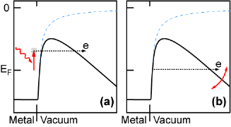
For weak optical fields, photoemission is dominated by the photofield effect Lee1973 , in which an initially bound electron is promoted in energy by through absorption of a single photon of frequency and subsequently tunnels to the continuum [Fig. 1(a)]. Due to the physical characteristics of the tunneling process, electron emission is prompt with respect to the incident electric field. For stronger optical fields, the local electric field associated with the optical field directly modifies the tunneling potential [optical field emission, Fig. 1(b)], again leading to prompt electron emission. We are able to continuously tune between the photofield and optical field emission regimes by varying the intensity of the driving laser. These prompt mechanisms compete with thermally induced emission, which takes place on time scales of tens of femtoseconds to picoseconds Fann1992 ; Riffe1993 ; Merschdorf2003 . We are able to find operating conditions where the thermal mechanisms are negligible.
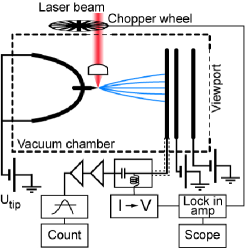
In our experiment, the output from a Kerr-lens mode-locked Ti:sapphire laser is focused on a field emission tip (Fig. 2). The laser operates at a 1 GHz repetition rate, and produces a train of 48 fs pulses (measured with an interferometric autocorrelator) at a center wavelength of 810 nm with maximum average power of 600 mW. The field emission tip is made of electro-chemically etched mm diameter tungsten single crystal wire in the (111) orientation. The tip is mounted in an ultra-high vacuum chamber and faces a micro channel plate detector (MCP) located 4 cm away from the tip. Field emitted electrons are accelerated onto the MCP detector. The amplified output is proximity focused on a phosphor screen. A CCD camera records the resulting image, which reflects the spatial distribution of photo-electrons. The time-of-arrival of amplified photo-electrons is obtained by monitoring the MCP bias current. At high MCP gains, we obtain spatial and temporal single electron detection resolution.
The local electric field strength at the tip is determined by the laser beam parameters (spot size, power, pulse duration and polarization), and local field enhancements due to plasmon resonances and lightning rod effects (see, for example, Martin2001 ). We focus the laser output to a m spot size ( radius) at the tip with an aspheric lens mounted within the vacuum chamber. The propagation vector of the laser beam is perpendicular to the tip shank, and an achromatic half-waveplate outside the chamber is used to control the beam’s polarization. We estimate that the focusing lens (mm) stretches the pulses to approximately 65 fs in the focus (see Kempe1992 ; Horvath1993 ), so that the peak intensity at the tip is For tungsten, the plasmon enhancements are relatively weak, while the lightening rod enhancement is 5 for a tip with a radius of curvature Martin2001 . Thus, we estimate the maximum electric field at the tip to be in excess of
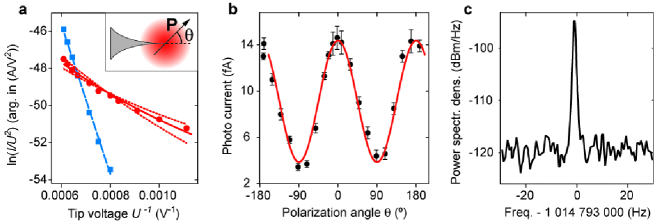
To experimentally determine the relevant emission mechanism, and in particular to demonstrate that electron emission is prompt with respect to the incident field, we studied emission characteristics as a function of the DC bias voltage, laser intensity and laser polarization. Fig. 3 shows emission data taken with a = 130 nm tip in the photofield regime. In (a) we measure the emitted current as a function of the tip bias voltage , both with and without the laser illumination. In both cases, data are fit to the Fowler-Nordheim equation Binh1996 , which relates the tunnel current density to the local electric field strength and the effective work function :
| (1) |
Here, is the electron charge, Planck’s constant, the electron mass, is a slowly varying function taking into account the image force of the tunneling electron, for field emission and is determined through with Gomer1961PlusComment . The electron current is related to the current density through with the radius of the emitter area.
We use the measurements without illumination and the known work function of tungsten to infer the tip radius Since does not change under laser illumination, we can then use this value to determine the effective work function when the tip is illuminated with the laser. We deduce that the effective work function is reduced by eV under illumination, which corresponds to the energy of the absorbed 810 nm laser photon. We verified that the value of the inferred effective work function was insensitive to laser power for low laser power. Fig. 3(b) shows the polarization dependence of the photocurrent, which exhibits a behavior, where is the angle between the tip shank and polarization vector for the field. This is indicative of optical excitation of surface electrons, since translation symmetry prohibits excitation by the field component parallel to the surface Venus83SurfSci . Note that for thermally increased field emission we also expect a sinusoidal variation of the photocurrent with polarization angle. However, from Fresnel’s equations we expect that for the given tip geometry and spot diameter the tip is heated less if the light polarization is parallel to the tip and therefore, that the current reaches a maximum at Hadley1985 . We indeed observed such a dependence in cw laser operation with a much smaller modulation depth. Fig. 3(c) displays the spectrum analysis of the electron current around the laser repetition rate; a 30 dB signal-to-noise ratio peak is evident at the laser repetition rate. Taken together, these results show that, for these parameters, the processes involved in the electron emission are dominated by photofield emission. Thus we infer that electron emission is prompt with respect to the laser pulse, and rule out possible thermal emission mechanisms associated with laser induced heating of the tip Hadley1985 ; Fann1992 ; Riffe1993 ; Merschdorf2003 . For V more than of the emitted electrons are photo-emitted.
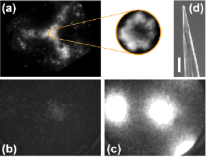
Decreasing the tip radius leads to smaller emission planes, and emission from a single atom is possible Fink88 ; Binh1996 ; Fu01 . Fig. 4(a) shows a field ion microscope (FIM) image of a 30 nm tip. The central emission plane is evident, consisting of a ring of 7 atoms and having an effective area of 2 nm diameter Tsong1990 . Fig. 4(b) shows the corresponding field emission (FEM) image at low bias voltage, without driving laser pulses. Each grain on the image indicates the detection of an individual electron. Emission from the central atom cluster is the dominant contributor to the photocurrent. Finally, Fig. 4(c) shows the same tip, at the same bias voltage, illuminated with laser pulses. In this image, the MCP is saturated due to the more than 100 times higher count rate. Although the count rates are substantially higher, the basic structure of the image is unchanged, indicating emission is coming from the sites identified in the FIM and non-illuminated FEM images. In this regime less than one electron is emitted per laser pulse. Due to the smallness of the emission area, such an electron beam is well suited to pulsed interferometer applications Kiesel2002 .
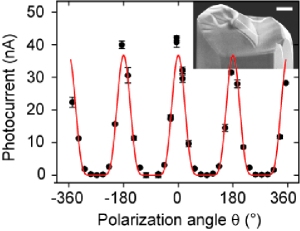
For applications which benefit from higher currents – but not necessarily atomic-scale localization of the emission sites – we investigated emission from blunt tips. Fig. 5 displays the polarization dependence of the emission current for a tip that ends in a flat m radius area, but which still exhibits sharp features for field enhancement Jersch1998FieldEnh . Under 530 mW illumination, time-averaged photocurrent rises to and is, as before, maximal when the field is parallel to the tip. In this case, however, the optical current exhibits a strong nonlinearity in the field component parallel to the tip and can be consistently fit to optical field emission behavior. In this case
| (2) |
Here, is the instantaneous absolute value of the laser field at the tip, the applied dc field, and and are constants. This expression is obtained from Eq. 1 by taking the local electric field to be the sum of the DC bias field and the incident laser field. Note that this expression is inherently time-dependent due to the presence of Since we measure the photocurrent time averaged over more than one optical cycle, we fit the data in Fig. 4 to Eq. 2 with replaced with assuming that electron emission is dominated by emission at the highest field strengths. Note that due to the exponential dependence of tunneling rate on the applied electric field, even modest intensity changes can dramatically alter emission characteristics. At this high laser power we find that sharper tips (nm) experience significant redistribution of emitting atoms, by comparing FIM images from before and after tip illumination. On average about 200 electrons per pulse are drawn from the tip for which corresponds to an instantaneous current of A or electrons per second. Assuming the electrons are emitted uniformly over 65 fs and over the entire surface, we can set a lower limit of on the instantaneous current density and a lower limit on the invariant brightness of . Both values are comparable to state-of-the-art electron pulses drawn from photocathodes in synchrotron electron sources King2005 .
In the future, we envision the techniques demonstrated in this work may lead to generation of sub-1 femtosecond pulses from single-atom tips by exploiting the non-linearity in the laser-tip interaction Baltuska2003 ; Niikura2002 . Likewise, this non-linearity might enable a direct measurement of the carrier-envelope phase of the laser pulse Paulus2003 ; Apolonski04 ; Fortier04 ; Sansone2004 . Since single atom tips have been shown to emit electrons via localized states with a lifetime in the range of a few femtoseconds Binh1992 ; Yu1996 , tip excitation with laser pulses of a similar or shorter duration in the optical field emission regime may lead to the development of deterministic single electron sources Zrenner2002 , which may have important applications in quantum information science. Finally, optimized nano-fabricated tip geometries may lead to sources of unprecedented emission brightness.
We are indebted to Mingchang Liu and Kai Bongs for assistance in the very early stages of this experiment and to Ralph DeVoe and Steve Harris for discussions. This work was supported by the ARO MURI program. P.H. thanks the Humboldt Foundation for a Lynen Fellowship and A. A.-T. the DAAD.
References
- (1) T. T. Tsong. Atom-probe field ion microscopy (Cambridge University Press, Cambridge, 1990).
- (2) R. Wiesendanger and H.-J. Güntherodt, eds. Scanning Tunneling Microscopy II (Springer, Berlin Heidelberg New York, 1992).
- (3) H. Kiesel, A. Renz, and F. Hasselbach. Nature 418, 392 (2002).
- (4) B. J. Siwick, J. R. Dwyer, R. E. Jordan, and R. J. D. Miller. Science 302, 1382 (2003).
- (5) H. Niikura, F. Légáre, R. Hasbani, A. D. Bandrauk, M. Yu. Ivanov, D. M. Villeneuve, and P. B. Corkum. Nature 417, 917 (2002).
- (6) H. Ihee, V. A. Lobastov, U. M. Gomez, B. M. Goodson, R. Srinivasan, C.-Y. Ruan, and A. H. Zewail. Science 291, 458 (2001).
- (7) W. E. King, G. H. Campbell, A. Frank, B. Reed, J. F. Schmerge, B. J. Siwick, B. C. Stuart, and P. M. Weber. J. Appl. Phys. 97, 111101 (2005).
- (8) O. Takeuchi, M. Aoyama, R. Oshima, Y. Okada, H. Oigawa, N. Sano, H. Shigekawa, R. Mota, and M. Yamashita. Appl. Phys. Lett. 85, 3268 (2004).
- (9) M. Merschdorf, W. Pfeiffer, A. Thon, and G. Gerber. Appl. Phys. Lett. 81, 286 (2002).
- (10) S. Grafström. J. Appl. Phys. 91, 1717 (2002).
- (11) M. J. G. Lee. Phys. Rev. Lett. 30, 1193 (1973).
- (12) W. S. Fann, R. Storz, H. W. K. Tom, and J. Bokor. Phys. Rev. B 46, 13592 (1992).
- (13) D. M. Riffe, X. Y. Wang, M. C. Downer, D. L. Fisher, T. Tajima, and J. L. Erskine. J. Opt. Soc. Am. B 10, 1424 (1993).
- (14) M. Merschdorf, W. Pfeiffer, S. Voll, and G. Gerber. Phys. Rev. B 68, 155416 (2003).
- (15) Y. C. Martin, H. F. Hamann, and H. K. Wickramasinghe. J. Appl. Phys. 89, 5774 (2001).
- (16) M. Kempe, U. Stamm, B. Wilhelmi, and W. Rudolph. J. Opt. Soc. Am. B 9, 1158 (1992).
- (17) Z. I. Horváth and Z. Bor. Optics Comm. 100, 6 (1993).
- (18) See, for example, V. T. Binh, N. Garcia, and S. T. Purcell. Adv. Imag. Elect. Phys. 95, 63 (1996).
- (19) We determine through an iterative routine, as described in R. Gomer. Field emission and field ionization (Harvard University Press, Cambridge, Massachusetts, 1961).
- (20) D. Venus and M. J. G. Lee. Surface Science 125, 452 (1983).
- (21) K. W. Hadley, P. J. Donders, and M. J. G. Lee. J. Appl. Phys. 57, 2617 (1985).
- (22) H.-W. Fink. Physica Scripta 38, 260 (1988).
- (23) T.-Y. Fu, L.-C. Cheng, C.-H. Nien, and T. T. Tsong. Phys. Rev. B 64, 113401 (2001).
- (24) J. Jersch, F. Demming, L. J. Hildenhagen, and K. Dickmann. Appl. Phys. A 66, 29 (1998).
- (25) A. Baltus̆ka, Th. Udem, M. Uiberacker, M. Hentschel, E. Goulielmakis, Ch. Gohle, R. Holzwarth, V. S. Yakovlev, A. Scrinzi, T. W. Hänsch, and F. Krausz. Nature 421, 611 (2003).
- (26) G. G. Paulus, F. Lindner, H. Walther, A. Baltŭska, E. Goulielmakis, M. Lezius, and F. Krausz. Phys. Rev. Lett. 91, 253004 (2003).
- (27) A. Apolonski, P. Dombi, G. G. Paulus, M. Kakehata, R. Holzwarth, Th. Udem, Ch. Lemell, K. Torizuka, J. Burgdörfer, T. W. Hänsch, and F. Krausz. Phys. Rev. Lett. 92, 073902 (2004).
- (28) T. M. Fortier, P. A. Roos , D. J. Jones, S. T. Cundiff, R. D. R. Bhat, and J. E. Sipe. Phys. Rev. Lett. 92, 147403 (2004).
- (29) G. Sansone, C. Vozzi, S. Stagira, M. Pascolini, L. Poletto, P. Villoresi, G. Tondello, S. DeSilvestri, and M. Nisoli. Phys. Rev. Lett. 92, 113904 (2004).
- (30) V. T. Binh, S. T. Purcell, N. Garcia, and J. Doglioni. Phys. Rev. Lett. 69, 2527 (1992).
- (31) M. L. Yu, N. D. Lang, B. W. Hussey, T. H. P. Chang, and W. A. Mackie. Phys. Rev. Lett. 77, 1636 (1996).
- (32) A. Zrenner, E. Beham, S. Stufler, F. Findeis, M. Bichler, and G. Abstreiter. Nature 418, 612 (2002).