Quantum Optics with Surface Plasmons
Abstract
We describe a technique that enables strong, coherent coupling between individual optical emitters and guided plasmon excitations in conducting nano-structures at optical frequencies. We show that under realistic conditions, optical emission can be almost entirely directed into the plasmon modes. As an example, we describe an application of this technique involving efficient generation of single photons on demand, in which the plasmon is efficiently out-coupled to a dielectric waveguide.
pacs:
32.80.-t, 03.67.-a, 42.50.Pq, 73.20.MfThe fields of quantum computation and quantum information science have spurred substantial interest in generating strong, coherent interactions between individual quantum emitters and photons. Such a mechanism would enable quantum information to be passed over long distances, which is essential for quantum communication ekert91 ; briegel98 and would facilitate the scalability of quantum computers svore04 . The required coupling between emitters and photons is difficult but has been achieved in a number of systems that reach the so-called “strong-coupling” regime of cavity quantum electrodynamics thompson92 ; brune96 . Recently, several approaches to reach this regime on a chip at microwave frequencies have been suggested childress04 ; sorensen04 ; blais04 ; wallraff04 and experimentally observed wallraff04 . A key feature of these approaches is the use of conductors to reduce the effective mode volume for the photons, thereby achieving a substantial increase in the coupling strength . Realization of analogous techniques with optical photons would open the door to many potential applications in quantum communication and in addition lead to smaller mode volumes and hence faster interaction times.
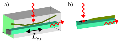
This Letter describes a method that enables strong, coherent coupling between individual emitters and electromagnetic excitations in conducting nano-structures at optical frequencies, via excitation of guided plasmons localized to nanoscale dimensions. The strong coupling is possible due to the small mode volume associated with this sub-wavelength confinement. We first examine the simple case of a conducting nanowire, where the relevant physical mechanisms can be understood analytically, and then consider an optimized geometry of a metallic nanotip. Because of dissipative losses in metals the plasmon modes themselves are not suitable as carriers of information over long distances. We show, however, that the plasmon excitation can be efficiently out-coupled through evanescent coupling with a nearby dielectric waveguide, as illustrated schematically in Fig. 1. This can be used, e.g., to create an efficient single photon source, or as part of an architecture to perform controlled interactions between distant qubits. We find that single-photon efficiencies exceeding are possible using relatively simple implementations.
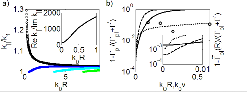
Surface plasmons smolyaninov03 are bound, non-radiative electromagnetic excitations associated with charge density waves propagating along the surface of a conducting object. For a smooth, cylindrical nanowire, it is convenient to write the fields in terms of cylindrical coordinates, , where denotes the regions outside and inside the metal, respectively. The functions are determined by Maxwell’s Equations along with appropriate boundary conditions and are given in stratton41 . The modes are characterized by the longitudinal component of the wave vector , which is related to the free-space wavevector , dielectric permittivity , and imaginary transverse wave vector by . is related to the inverse decay length of the field away from the surface. The dependence of for a conducting wire on its radius is shown in Fig. 2(a), for a few lowest order modes. Throughout this paper, all figures and numbers presented use the optical properties of silver () johnson72 at a vacuum wavelength m, and assume a surrounding dielectric .
For a conducting nanowire (), there exists one, fundamental TM mode takahara97 ; jahns05 with axial symmetry (), while all higher-order modes are cut off. For this mode, , indicating that the phase velocity is greatly reduced while the transverse mode area is localized to a region on the order of the wire size. The proportionality constant depends only on and is given by
| (1) |
where is Euler’s constant. This sub-wavelength guiding of plasmons in metal nanowires has recently been observed in a number of experiments dickson00 ; krenn02 ; ditlbacher05 .
At optical frequencies a conductor has finite losses characterized by , resulting in dissipation of the plasmon wave at a rate given by . Due to the tighter localization, decreases and approaches some non-zero value () as , as shown in the inset of Fig. 2(a) for the fundamental mode. Physically is proportional to the number of plasmon wavelengths the plasmon will travel before decaying.
We now consider the emission properties near a nanowire of an oscillating dipole, which physically can be formed by a single atom, a defect in a solid-state system, or any other system with a dipole-allowed transition. This dipole can generally lose its excitation radiatively by emitting a photon, non-radiatively through dissipation of currents induced by the dipole in the metal, or into the guided plasmon modes. It is well-known that the corresponding spontaneous emission rates can be obtained via classical calculations of the fields wylie84 . For sub-wavelength systems this calculation further simplifies because it is sufficient to consider the quasi-static () field solutions klimov04 , the derivation of which we outline here. Given a point charge source at outside the metal, we write the static potential outside in terms of the free-space potential and a reflected component, , while gives the potential inside the wire. Note that the potential due to a dipole at is easily found from the point source potential via . Since are solutions to the Laplace equation, , we can expand in an appropriate basis,
| (2) |
where are arbitrary coefficients, and are modified Bessel functions. A similar expansion holds for , with the replacements and . Expanding in a similar basis, algebraic equations for result by requiring that at the boundary and that is continuous here. The solution for is found to be
| (3) |
The radiative decay rate is determined by finding the dipole contribution to at large distances , which for a nanowire is due to the term in Eq. (2). Physically corresponds to an induced dipole moment in the nanowire, and leads to a modified radiative decay rate . The non-radiative and plasmon decay rates can be calculated via , where is the total field at the dipole location. In the limit that the distance between emitter and wire edge approaches zero, one finds that diverges due to a substantial contribution from the sum over in Eq. (2). This term is proportional to and can thus be identified with non-radiative decay. At the same time, Eq. (3) exhibits a pole in that corresponds to excitation of the fundamental plasmon mode, and whose contribution to yields the plasmon decay rate. For a nanowire, the radiative and non-radiative decay rates for a dipole oriented along are given by klimov04
| (4) | |||||
| (5) |
where is the decay rate in uniform dielectric note2 , while the plasmon decay rate is tobepublished
| (6) |
is a complicated expression but depends only on .
The scalings of the various decay rates can be intuitively understood. Away from the plasmon resonance (), varies slightly from due to a small change in the radiative density of states near the nanowire, while the dependence in reflects the dissipation of a divergent current induced in the nanowire by the near-field of the dipole. The scaling for can be understood from Fermi’s Golden Rule, , where is the position-dependent coupling strength between emitter and plasmon modes and is the plasmon density of states on the wire.
The position dependence of the decay rates results in an optimal emitter distance for which the probability of decay into plasmons is maximized, where denotes the total “non-plasmon” decay rate. For typical parameters, is on the order of several as , such that the emitter sits within the localized plasmon field but is not too close to the wire that dissipation become dominant. In Fig. 2(b) we plot the probability of emission into non-plasmon channels, , as a function of when the optimal is chosen. This optimized “error” rate decreases monotonically as and approaches a small number indicating that the efficiency of emission into plasmons is ultimately limited by dissipative losses. As , one can achieve effective Purcell factors of for a silver nanowire.
The nanowire is a simple system that illustrates the relevant properties of dipole emission and plasmon propagation. One immediately sees, however, that the increase in coupling achieved by letting is accompanied by a decrease in the plasmon propagation length, which limits coherent processes of interest. Such limits can be circumvented with simple design improvements, which we illustrate specifically for the case of a metallic nanotip, assumed to have a paraboloidal profile given by (). One expects a similar enhancement of plasmon emission due to the nanotip, yet the tip can quickly expand to larger radii where losses can be significantly reduced. As in the nanowire case, one can calculate the emission rates based on the quasi-static field solution of a dipole near a tip, which is exactly solvable by working in parabolic coordinates. For an emitter located on-axis at position and oriented along , we find that tobepublished
| (7) | |||||
| (8) | |||||
| (9) |
Here, is a constant that again only depends on , and is the solution to Eq. (1). From these decay rates one finds an optimized Purcell factor as , as shown in Fig. 2(b), for the same material parameters as the nanowire calculation. In the case of a nanotip, however, we are primarily interested in the probability that the plasmon propagates up to some final radius . We estimate this quantity by making an eikonal approximation based on the nanowire solution stockman04 . In particular, we assume that the plasmons are completely emitted into the end of the tip () at a rate , while the rate at which the plasmon emission successfully propagates to some larger radius is given by
| (10) |
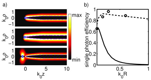
Here is the nanowire solution at radius . In Fig. 2(b) we plot as a function of , optimized over the emitter position and . This quantity corresponds to an effective error probability in which the plasmon mode is either not excited or fails to successfully propagate to some final radius . For the tip leads to significant improvement in efficiency compared to nanowires of the same . To check the validity of these approximations we have performed numerical (electrodynamic) simulations of dipole emission near a nanotip using boundary element method abajo02 , with the resulting numerically optimized plotted in Fig. 2(b). It can be seen that the theory agrees well with the numerics. Some typical simulation results are shown in Fig. 3(a). Here we plot for different emitter positions the quantity , which is proportional to the energy flux of the system normalized by the total power output of the emitter. It can clearly be seen that choosing the optimal position results in efficient excitation of the plasmons at final radius , while other positions can result in primarily non-radiative or radiative decay.
Because of losses, the plasmon modes are not suitable as carriers of information over long distances. However, one can evanescently couple the plasmons to dielectric waveguide modes, which can form an architecture for a device to generate single photons on demand. Noting that the concepts behind single photon generation with a single emitter in a cavity have been presented in detail elsewhere cirac97 ; michler00 ; pelton02 ; mckeever04 , here we illustrate a potential novel realization of a single photon device, shown in Fig. 1(a). In this architecture, a single, optically addressable emitter such as a quantum dot sits atop a nanowire, which co-propagates over some length with a nearby dielectric waveguide. In order to maximize the transfer efficiency into the waveguide, the longitudinal wavevectors of the plasmon and waveguide should be approximately matched, and should be optimized. In practice, for a given wire radius , the matching condition results in some optimization of parameters such as the waveguide size. A similar setup using a nanotip instead of a nanowire is illustrated in Fig. 1(b). Here the nanotip maintains a paraboloidal profile up to some final radius , at which point it becomes a straight nanowire supporting plasmon modes with well-defined that can be easily be mode-matched with the waveguide.
The out-coupling and single photon efficiencies can be calculated using standard mode-coupled equations based on Lorentz reciprocity barclay03 . For simplicity, we take the dielectric waveguide to be a cylindrical optical fiber, whose modes can be calculated analytically stratton41 , and set the surrounding and fiber core permittivities to be . In Fig. 3(b), we plot the optimized efficiency for single photon generation as a function of , for both the nanowire and nanotip, based on the decay probabilities obtained above and coupled-mode theory. We also include the predicted efficiencies using the boundary element method simulations combined with coupled-mode theory. These calculations take fully into account all imperfections, including metal losses and imperfect waveguide coupling. We observe that there is some optimal where is maximized, which corresponds to a balance between achieving large coupling between emitter and nano-structure, and ensuring that the plasmon/guide coupling exceeds the enhanced losses at small . We find that optimal single photon efficiencies exceeding are achievable in such a system.
Such an architecture for quantum communication based on plasmonic devices has several important features. First, unlike typical methods of cavity QED, the plasmon excitation covers a broad bandwidth and requires no special tuning to achieve resonance. The operation speeds can also be quite high because of the sub-wavelength mode volumes associated with the plasmons. Finally, we note that rapid advances in recent years in fabrication techniques for nanowires xia02 ; schultz02 , nanotips libioulle95 , and sub-wavelength dielectric waveguides tong03 ; vlasov04 puts such a system in experimental reach.
The authors thank Atac Imamoglu for useful discussions. This work was supported by the ARO-MURI, ARDA, NSF, the Sloan and Packard Foundations, and by the Danish Natural Science Research Council.
References
- (1) A.K. Ekert, Phys. Rev. Lett. 67, 661 (1991).
- (2) H.-J. Briegel et al., Phys. Rev. Lett. 81, 5932 (1998).
- (3) K.M. Svore, B.M. Terhal, and D.P. DiVincenzo, e-print quant-ph/0410047 (2004).
- (4) R.J. Thompson, G. Rempe, and H.J. Kimble, Phys. Rev. Lett. 68, 1132 (1992).
- (5) M. Brune et al., Phys. Rev. Lett. 76, 1800 (1996).
- (6) L. Childress, A.S. Sørensen, and M.D. Lukin, Phys. Rev. A 69, 042302 (2004).
- (7) A.S. Sørensen et al., Phys. Rev. Lett. 92, 063601 (2004).
- (8) A. Blais et al., Phys. Rev. A 69, 062320 (2004).
- (9) A. Wallraff et al., Nature 431, 162 (2004).
- (10) For a review, see, e.g., A.V. Zayats and I.I. Smolyaninov, J. Opt. A 5, S16 (2003).
- (11) J.A. Stratton, Electromagnetic theory, 1st ed. (McGraw-Hill, New York, 1941), Chapter 9.
- (12) J. Takahara et al., Opt. Lett. 22, 475 (1997).
- (13) See also recent work in the terahertz domain, e.g., Q. Cao and J. Jahns, Opt. Express 13, 522 (2005).
- (14) R.M. Dickson and L.A. Lyon, J. Phys. Chem B 104, 6095 (2000).
- (15) J.R. Krenn et al., Europhys. Lett. 60, 663 (2002).
- (16) H. Ditlbacher et al., Phys. Rev. Lett. 95, 257403 (2005).
- (17) P.B. Johnson and R.W. Christy, Phys. Rev. B 6, 4370 (1972).
- (18) See, e.g., J.M. Wylie and J.E. Sipe, Phys. Rev. A 30, 1185 (1984).
- (19) V.V. Klimov and M. Ducloy, Phys. Rev. A 69, 013812 (2004).
- (20) Here we take , where is the spontaneous emission rate in vacuum. See, e.g., S. Scheel et al., Phys. Rev. A 60, 1590 (1999).
- (21) D.E. Chang, A.S. Sørensen, P.R. Hemmer, and M.D. Lukin, quant-ph/0603221.
- (22) Such an approach was used to study nanofocusing of energy in metallic tips, in M.I. Stockman, Phys. Rev. Lett. 93, 137404 (2004).
- (23) F.J. Garcia de Abajo and A. Howie, Phys. Rev. B 65, 115418 (2002).
- (24) J.I. Cirac et al., Phys. Rev. Lett. 78, 3221 (1997).
- (25) P. Michler et al., Science 290, 2282, (2000).
- (26) M. Pelton et al., Phys. Rev. Lett. 89, 233602 (2002).
- (27) J. McKeever et al., Science 303, 1992 (2004).
- (28) P.E. Barclay, K. Srinivasan, and O. Painter, J. Opt. Soc. Am. B 20, 2274 (2003).
- (29) Y. Sun et al., Nano Lett. 2, 165 (2002).
- (30) M. Barbic et al., J. Appl. Phys. 91, 9341 (2002).
- (31) L. Libioulle, Y. Houbion, and J.-M. Gilles, J. Vac. Sci. Technol. B 13, 1325 (1995).
- (32) L. Tong et al., Nature 426, 816 (2003).
- (33) Y.A. Vlasov and S.J. McNab, Opt. Express 12, 1622 (2004).


