A simple quantum gate with atom chips
Abstract
We present a simple scheme for implementing an atomic phase gate using two degrees of freedom for each atom and discuss its realization with cold rubidium atoms on atom chips. We investigate the performance of this collisional phase gate and show that gate operations with high fidelity can be realized in magnetic traps that are currently available on atom chips.
pacs:
03.67.LxQuantum computation and 34.90.+qOther topics in atomic and molecular collision processes and interactions and 52.55-sMagnetic confinement and equilibrium1 Introduction
Neutral atoms are promising candidates for the physical implementation of quantum information processing (QIP). The weak interaction of neutral atoms with their environment leads to long coherence times, and mature experimental techniques from quantum optics and atomic physics allow to prepare and manipulate atomic quantum systems.
In recent years new tools for the precise control and manipulation of neutral atoms were developed, based on the adaption of microfabrication techniques to atom optics and the implementation of the atom chip Fol02 . Such atom chips apply the advantages of micro-fabrication technology from micro-electronics and micro-optics to atomic physics with the goal to build integrated devices for quantum manipulation of ultra-cold atomic samples and a collection of single atoms.
In the quest for implementations of QIP with neutral atoms, atom chips are promising candidates for a number of reasons: (i) Large electric and magnetic field gradients and field curvatures near microscopic conductors lead to tight confinement and large energy level spacings for the trapped atoms (trap frequencies in the range of hundreds of kHz were implemented Fol00 ). (ii) Very high resolution of the potentials (sub-m) can be implemented when going close to the surface (m distance). This is important for QIP proposals in which the short distances (order of 1 m) between individual trapping sites is required to achieve sizable qubit coupling and fast gate operations. (iii) Nanofabrication techniques on surfaces facilitate accurate and robust placement of structures with size limit well below 100 nm. This enables the realization of nearly arbitrary potential configurations. (iv) Integration of new components, for example micro-optics and micro-cavities for preparation, manipulation, and detection of qubits are possible. (v) Last, but not least, nanofabrication schemes are particularly well suited for production of multiple structures.
In this paper we discuss in more detail how to implement a quantum logic operation with the toolbox of atom chips. We will make thereby use of two different degrees of freedom, each of them having two levels, for each qubit. We use the first degree of freedom to storage information and the second one to process it. This helps to take advantage of the best features of both degrees of freedom. One pair of states (the hyperfine levels of a trapped atom) will be used to storage the qubit, and the quantum gate operations will make use of two vibrational levels of the atom trap as qubit states and the collisions that realize the phase gate will occur in the same internal states, which has the advantage of reducing unwanted collisional losses. Our scheme therefore combines the important feature of long lived coherence of the hyperfine states with the phase gate operation with vibrational states via collisions.
We shall first discuss the implementations of qubits on atom chips, and then describe new schemes for implementing a phase gate for cold neutral atoms on atom chips. The results of a realistic calculation of the gate performance using typical state of the art atom chip parameters is given in Section 5. Section 6 briefly illustrates future directions of QIP on atom chips.
2 The Qubit
We shall discuss here only implementations where each qubit is written into a single atom. There are two distinct ways to encode a qubit into a single neutral (Rb) atom on atom chips:
-
•
The qubit is encoded into a pair of long-lived internal states such as two different hyperfine ground states of an atom. The qubit states have to be trappable on the atom chip, and show long coherence times.
To achieve long coherence times, it is advisable to use atomic states where the energy difference is to first order independent of external fields (clock states). In free space these would be the and states used in atomic clocks, which show only quadratic Zeeman and Stark shifts. On the atom chip one can achieve the same common mode rejection of external field noise using the hyperfine levels and of the ground state of 87Rb which have the same magnetic moment at a magic magnetic field of G Cornell . Operating a trap at this offset field, the energy difference between these two trapable states shows only a quadratic dependence on external field fluctuations like the clock states at zero field.
Single-qubit operations are induced as transitions between the hyperfine states of the atoms. These can be driven by external fields, using radiofrequency (RF) and/or microwave (MW) pulses or optical Raman transitions. As an example we mention the atom chip experiment in Munich rei1 which demonstrated the very long coherence times in a magnetic atom chip trap for the special clock states and at a trapping magnetic field near the value .
-
•
The qubit is encoded in external, motional states of the atom in a tight trap. These motional states can be either the ground and an excited state in a trap, or the left and right states of a double well. In such a realization the atoms are in the same internal state, and therefore automatically isolated from external fluctuations. Single-qubit operations are then Rabi rotations between the motional states, and can be seen like trapped atom interferometers.
To implement a quantum bit on an atom chip, the qubit states have to be trappable, and show long coherence times. That is we require a common mode rejection of external field noise (clock states). Atoms trapped in different motional states are easier to state-selectively manipulate, but much less is known on external state decoherence, and how to prevent it.
3 New schemes for a phase gate
The phase gate is a two-qubit quantum gate described by the evolution operator nielsen
Several different implementations of this universal gate have been proposed. In particular, schemes where internal electronic states of atoms are the logic states and and state-dependent atomic collisions generate appropriate values of the phase (usually ) have been discussed cala ; tren ; delo ; will . In these cases the correct performance of the phase gate requires that at some time all vibrational states have a complete revival up to a phase.
Our schemes use two different degrees of freedom, each of them having two levels, for each qubit. We use the first degree of freedom to storage information and the second one to process it. The “storage” qubit levels are denoted as and , whereas the “operation” qubit levels are denoted as and . Such a scheme helps to take advantage of the best features of both degrees of freedom.
In principle, the qubit operations we shall describe can be performed directly on the storage states, so our schemes might appear as an unnecessary complication.
In the specific scheme presented here, the storage qubit is encoded in the clock states and of the ground state of 87Rb. Quantum coherences between these two states have been demonstrated with decoherence times exceeding 1 s rei1 when the value of the trapping magnetic field is set to the magic value . However, these clock qubit states are trapped in identical trapping potentials. Direct realizations of the phase gate via internal state-dependent time-varying potentials like the one described in cala are hence not feasible. For this reason, we choose two vibrational states as operation qubit states as suggested in delo ; will in order to realize a collisional phase gate that does not rely on the internal states.
This approach combines the important feature of long coherence time of the hyperfine states with the phase gate operation with vibrational states via collisions. The storage states are the hyperfine levels and , the operation states and are the ground and first excited states of the atomic vibrations, respectively. The MW-RF two-photon transitions described in rei1 can be used for single qubit operations on the storage states. For a two-qubit phase gate, our schemes can be summarized as follows: the logic state is encoded and stored in the hyperfine states; when two-qubit gate operation must be performed, the logic state is transferred into the vibrational states and the gate operation takes place via collisions; at the end of the operation, the logic state of the vibrations is transferred back into the internal hyperfine states.
There are two different ways to realize this idea. We can (a) duplicate the logic state of the storage levels in the vibrational levels or (b) swap the logic states of the two degrees of freedom.
The duplication scheme (a) for the phase gate is summarized by the map
| (2) | |||||
| (3) | |||||
| (4) | |||||
| (5) |
whereas the swap scheme (b) is summarized by
| (6) | |||||
| (7) | |||||
| (8) | |||||
| (9) |
Let’s assume that information is initially encoded in two storage levels of two qubits,
| (10) |
which may be already entangled. The duplication scheme takes place in three steps: (i) We selectively excite the (vibrational) operation state,
| (11) |
(ii) only the two states collide, acquiring a dynamical phase equal to
| (12) |
like in cala ; tren ; delo ; will , where only the two excited (vibrational or internal) states get a collisional phase on top of the kinematic phase; finally (iii) we de-excite (selectively) the operation state:
| (13) |
In this way the result of the phase gate operation on the operation states is transfered to the storage states. The second alternative scheme swaps the storage and operation states for the phase gate performance. Starting from the initial state Eq.(10), again three steps are required for the gate operation: (i) we selectively excite the operation state and de-excite the storage states
| (14) |
i.e, we swap their logic states; then (ii) the operation states get a dynamical phase equal to
| (15) |
through collisions as in the duplication scheme; finally (iii) we swap again the storage and operation states
| (16) |
These schemes are not restricted to internal and external degrees of freedom of cold atoms, but can be applied to any system with at least two degrees of freedom.
The duplication scheme does not modify the storage states. During the phase gate operation (Eq. 12), the storage and the operation states are entangled. In the swap scheme, on the other hand, the storage states are modified but the two (storage and operation) degrees of freedom remain always separable.
4 Excitations of vibrations of hyperfine states of neutral atoms
The two schemes for a phase gate described in the previous section require a selective excitation of vibrational states when implemented with cold atoms. We specialize our discussion to 87Rb atoms, having mass kg, confined in traps of frequency kHz and higher. Two-photon Raman processes have already been used for sideband excitations of trapped ions in the Lamb-Dicke regime wine and are natural candidates also to excite vibrational states of neutral trapped atoms. So we examine the transitions from an initial state to a final state driven by two external radiation fields through an intermediate state which is never populated. From the Hamiltonian of a three-level atom interacting with two radiation fields an effective two-level Hamiltonian
| (17) |
is obtained, where and and are the wave vectors of the two driving fields, is the effective Rabi frequency, is the detuning of the two fields from the transition frequencies , . The factors are the Rabi frequencies of the transitions and . The effective Hamiltonian (17) is obtained under the hypotheses . The atomic motion is quantized when we write
| (18) |
where and are the usual annihilation and creation operators of the harmonic oscillator and
| (19) |
is the Lamb-Dicke parameter.
The two-photon process can be obtained either through MW and RF transitions involving other hyperfine levels of the ground state or through optical transitions involving a hyperfine level of the excited state. Microwave transitions between the hyperfine states occur at the frequency GHz, so is of the order of , well within the Lamb-Dicke limit. The effective Hamiltonian Eq.(17) can then be approximated by a Jaynes-Cummings Hamiltonian
| (20) | |||||
where the rotating wave approximation has been used and the eigenstates , with energies , of the atomic motion have been included comm . In Eq.(20) the sideband Rabi frequency replaces the effective Rabi frequency . Since the effective Rabi frequency can easily be increased up to kHz treu , the sideband Rabi frequency has an upper bound of the order of Hz. Microwave transitions would then occur rather slowly.
Optical transitions employing the or level as intermediate state have wavelengths of the order of nm. The upper bound of the Lamb-Dicke parameter is . The Lamb-Dicke regime necessary for sideband excitation requires either the choice of appropriate directions of the the wave vectors and of the two radiation fields or trapping frequencies above Hz. The ongoing miniaturizations of atom chip structures have reached this range of frequencies Fol00 .
In the duplication scheme only the vibrational state must be modified. The desired transition is , the energy difference of which gives the sideband excitation condition . Microwave Raman processes where the ground state is the intermediate state would ensure selectivity, but the Rabi oscillations would be slow, as mentioned before. On the other hand, the optical transitions do not fulfill the selectivity requirement, since the lasers that drive the transitions would also drive the undesired transitions (only the detuning of the two transitions would be slightly different). The duplication schemes presents severe drawbacks for the system we are considering.
In the swap scheme both the internal and the vibrational states are changed, so the desired sideband excitation requires . This condition differs from the condition of the undesired sideband excitation by the small amount , so the radiation linewidth must be tight enough to prevent the undesired transition . This condition is reached experimentally by standard techniques which allow to reduce the linewidths appropriately. Specific pulse shaping techniques can be used to ensure an optimal probability of the correct transition even for short pulses. Moreover, the logic states and can be equivalently encoded in each of the two hyperfine clock states. The swap scheme with optical transitions suits better neutral 87Rb atoms trapped on atom chips than the duplication scheme.
5 Magnetic traps on atom chips and phase gate operation
To implement a phase gate between two qubit sites on an atom chip we consider a very simple double well configuration. The two qubits are trapped in the two wells respectively, and they can interact via the barrier.
In this paper we consider the simplest of these geometries for the quantum gate implementation in magnetic micro traps on an atom chip, the H configuration rei2 (see Fig.1). Here one wire along the axis ( wire) carries a current and two parallel wires along the axis (left and right wire), separated by a distance , carry a current ; a bias magnetic field parallel to the surface is employed. Appropriate values of currents and bias field create the magnetic trapping potentials for neutral atoms. In the approximation of infinitely long and thin wires, with negligible separation along the axis, the wire and the bias field produce a trapping field
| (21) |
and the two parallel wires produce the localization fields
| (22) |
where and is the vacuum permeability.
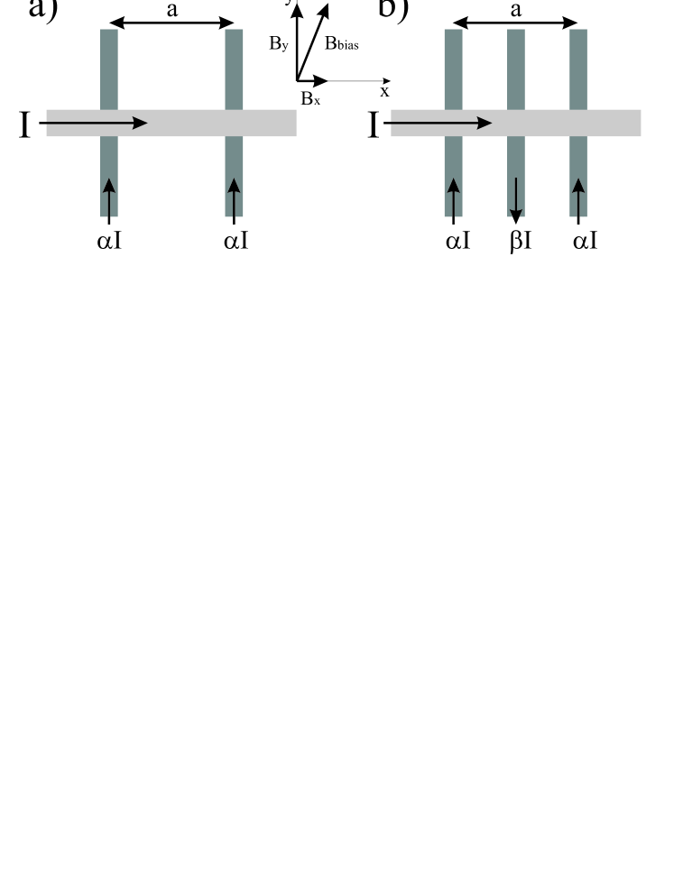
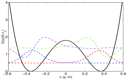
By using realistic parameters that have been tested in current atom chips and setting m, mA, , G, and G, we find a trapping potential for two atoms (Fig. 2), with two minima and lying on an axis rotated by an angle with respect to the axis. The magnetic field in the two minima has the desired value G. The trap frequencies in the two minima are kHz along the direction of longitudinal confinement, kHz, and kHz along the direction of transverse confinement. Atoms in the transverse ground state will perform one-dimensional (1D) dynamics along the axis only. The 1D potential is shown in Fig.2. The distance of the two minima from the chip surface is m; the separation of the two minima is about m. The variation of the magnetic field along the trapping potential is small: at the maximum height of the central barrier we have G.
We have used this static magnetic potential to study the performance of a collisional phase gate. Steps (i) and (iii) of the swap scheme require an optical two-photon transition, as already discussed in Section 4. The probability to populate the second excited vibrational level is about % of the probability of sideband excitation of the first excited vibrational level, thus affecting the fidelity of the operation. In our simple scheme, the value % results from the anharmonicity of the longitudinal trapping potential, and represents a lower limit that cannot be reduced with a further decrease of the Lamb-Dicke parameter. In the Lamb-Dicke regime the ratio of the two probabilities
| (23) |
becomes independent of the Lamb-Dicke parameter. Nevertheless the probability of this undesired transition can be further decreased with an optimal modulation of the trapping potential in more complex schemes that go beyond the simple gate investigated here. For example, if one starts with a high barrier separating the two wells, the vibrational states under considerations are much better approximated by harmonic oscillator states and thus the excitation of the higher vibrational states in the Lamb-Dicke regime is essentially suppressed since .
The realization of step (ii) of the swap scheme in the trapping potential in Fig.2 can also be considered as a simplified version of the phase gate proposed in will . The ground and first excited vibrational states of each potential well are the logic states. These states are linear superpositions of eigenstates of the trapping potential; free atoms would tunnel from one well to the other. The presence of one atom in each well and their mutual interaction when they collide modifies significantly the dynamics. The choice of the trapping potential of Fig.2 combines two opposite requirements: the ground states must be deep in the well to avoid tunneling during the gate operation, while the excited states have to interact in order to develop the correct value of the phase .
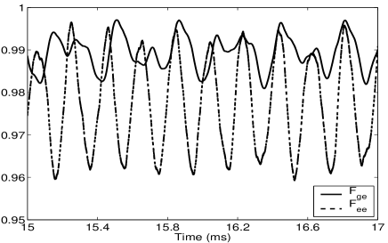
We have already discussed how to transfer the logic states from the storage qubit to the operation qubit. We examine now the gate operation performed with the vibrational states. Initially one atom sits in each well and the phase gate operation is performed via tunneling of the first excited states of the two atoms. A correct operation of the phase gate requires a complete revival (up to a phase) of each of the initial states , , (this state is simmetric of so we shall neglect it) and at some later time , as well as the fulfillment of the condition ( is the phase of the state ) at the same time . We solve the two-particle Schrödinger equation numerically in 1D with the split operator technique spli , replacing the scattering length of the hyperfine state of 87Rb with an effective scattering length that takes into account the transverse confinement cala . The interaction between the atoms is described by a contact potential, like in cala ; tren . After an operation time ms, the initial states and have an almost complete revival, with fidelities , (see Fig.3); moreover, the state is stationary on this time scale.
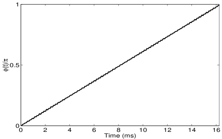
We have also evaluated the gate phase accumulated during the gate operation, and the final result is (see Fig.4).
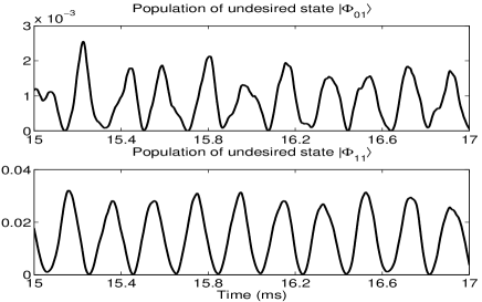
The populations of undesired states and , where the atoms are in the ground and first excited vibrational level of the same well, must be negligible. Our calculations confirm that these populations remain small (see Fig.5). These results also show that the effects of tunneling, that would increase the populations of the undesired states in the absence of interaction, are significantly reduced, as already stressed in will .
These results are encouraging, since they are obtained with realistic parameters and without introducing approximations for numerical convenience. The use of the clock states and greatly reduces the impact of fluctuations of the magnetic field due to current fluctuations, that would spoil the gate performance. Moreover, the use of a static trapping potential has the advantage of avoiding the necessity of accurate control over the relevant parameters (currents, magnetic fields, etc.) as requested by dynamic schemes. More complex approaches might further increase gate performances and reduce the operation time. We briefly discuss them in the next section.
6 Future perspectives
Atom chips provide the setup for a rich variety of traps for neutral atoms. In this paper we have discussed the simplest static magnetic potential for implementing quantum gates. Much more involved wire configurations can be thought of, electric fields coupling to the electric polarizability of the atom () can be brought in as additional design freedom last , RF and MW fields coupling different atomic states can be used to create adiabatic potentials and (slowly varying) time-dependent potentials will increase the versatility of qubit manipulation.
A first extension will be to use a three wire configuration as shown in Figure 1b which allows more freedom in designing the double well potential for qubit coupling. The wire in the middle can be used to control the barrier either by current or by electric fields. A time varying barrier potential height will allow techniques from quantum control Skl02 to be applied, and we expect a significant increase in the speed and fidelity of the quantum gate.
Encoding the qubit in different hyperfine states, like and of 87Rb, which have different interactions with magnetic fields but which couple equally to electric fields, will allow to use electric fields for state dependent collisions in two qubit operations. A combination of both magnetic and electric interactions allows to have a barrier between the state, and a collisional interaction between the states, thus opening the possibility of state-dependent dynamics. The drawback here is that we now have to deal with field sensitive qubits. This implies a demand for excellent magnetic field stability.
Even more versatile manipulation can be achieved by using the adiabatic potentials created by RF and MW fields to manipulate atoms garra . In an atom chip setup such RF or MW potentials have the distinct advantage, that one applies RF and MW near fields with a specific well defined polarization which is given by the wire configuration on the chip. At the relevant scales of the atom chip () propagation effects can be neglected and the fields can be calculated in a quasi static approximation.
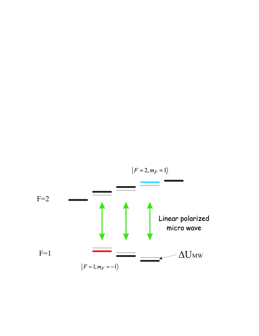
The coupling strength to the MW (RF) field is then given by the Rabi frequency . In the case of large detuning () the adiabatic potential can then be calculated as . Applying linear polarized MW radiation detuned from the hyperfine transition will create opposite potential shifts for the two hyperfine manifolds. This result in opposite sign MW potentials for two clock states and of 87Rb rei1 . Applying this MW field to a wire between the two trapping wires (the center wire in the 3 wire configuration of Fig. 1b) it will be possible to create state dependent potential barriers on the chip, which will greatly enhance the qubit manipulation capabilities.
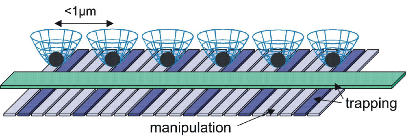
The above simple two qubit potentials and operations can be geralized to a atom chip quantum processor on an array of qubits. We envision such more advanced qubit manipulation on the atom chip (Fig. 7) to consist of an array of trappable qubits, consisting of single atoms trapped in tight traps. The strong transverse confinement will be created by a tight magnetic wire trap, the qubit sites can then be determined either by electrical leads or by crossed wires, as in the case considered here. In between these trapping sites we will have additional wires and electrodes for qubit manipulation and gate operations. these would create the barriers for qubit coupling and qubit isolation. At the end the qubit array can be read out by transporting the atoms one by one to an integrated micro cavity atom detector horak03 , reading their internal state.
7 Summary and Conclusions
We have discussed new simple scheme for implementing a phase gate on an atom chip. These schemes make use of two degrees of freedom for each qubit. Quantum information is stored in one degree of freedom and processed in the other. We have discussed the feasibility of realizing these schemes with cold 87Rb atoms magnetically trapped on atom chips, where the internal states are used to storage and the external (vibrational) states to process information, respectively. We have also investigated the performance of such schemes in atom chip traps with realistic parameter values. High fidelity gate operations are obtainable, thus showing that micro traps on atom chips are a very interesting candidate for quantum engineering and quantum information processing. Our investigations have concentrated on the most basic example of the many potential applications of micro traps on atom chips. Some more involved schemes are discussed as possible future developments.
Acknowledgements.
This work was supported by the European Union, contract numbers IST-2001-38863 (ACQP), MRTN-CT-2001-50532 (AtomChips), and the Deutsche Forschungsgemeinschaft, Schwerpunktprogramm ‘Quanteninformationsverarbeitung’. We thank M. Andersson, E. Charron, A. Recati, P. Treutlein for useful discussions.References
- (1) R. Folman, P. Krüger, J. Schmiedmayer, J.Denschlag, C. Henkel, Adv. At. Mol. Opt. Phys. 48, 263 (2002).
- (2) R. Folman et al., Phys. Rev. Lett. 84, 4749 (2000).
- (3) H. J. Lewandowski, D. M. Harber, D. L. Whitaker, and E. A. Cornell, Phys. Rev. Lett. 88, 070403 (2002); D. M. Harber, H. J. Lewandowski, J. M. McGuirk, and E. A. Cornell, Phys. Rev. A 66, 053616 (2002).
- (4) P. Treutlein, P. Hommelhoff, T. Steinmetz, T. W. Hänsch, and J. Reichel, Phys. Rev. Lett. 92, 203005 (2004); Phys. Rev. Lett. 93, 219904(E) (2004).
- (5) M. A. Nielsen and I. L. Chuang, Quantum Computation and Quantum Information (Cambridge University Press, Cambridge, 2000).
- (6) T. Calarco et al., Phys. Rev. A 61, 022304 (2000).
- (7) A. Negretti, T. Calarco, M. A. Cirone, and A. Recati, Eur. Phys. J. D 32, 119 (2005).
- (8) J. Mompart, K. Eckert, W. Ertmer, G. Birkl, M. Lewenstein, Phys. Rev. Lett. 90, 147901 (2001).
- (9) E. Charron, E. Tiesinga, F. Mies, C. J. Williams, Phys. Rev. Lett. 88, 077901 (2002).
- (10) D. M. Meekhof et al., Phys. Rev. Lett. 76, 1796 (1996).
- (11) The first term of the series expansion leads to a new definition of the internal eigenstates and their frequencies. For ease of notation, we continue to denote them with , and , .
- (12) P. Treutlein, private communication.
- (13) J. Reichel, W. Hänsel, P. Hommelhoff, T. W. Hänsch, Appl. Phys. B 72, 81 (2001).
- (14) See for instance B. M. Garraway and K.-A. Suominen, Rep. Prog. Phys. 58, 365 (1995).
- (15) O. Zobay and B. M. Garraway, Phys. Rev. Lett. 86, 1195 (2001).
- (16) P. Krüger et al., Phys. Rev. Lett. 91, 233201 (2003).
- (17) S. Sklarz and D. Tannor, Phys. Rev. A 66, 053619 (2002)
- (18) P. Horak et al., Phys. Rev. A 67, 043806 (2003).