Transporting, splitting and merging of atomic ensembles in a chip trap
Abstract
We present a toolbox for cold atom manipulation with time-dependent magnetic fields generated by an atom chip. Wire layouts, detailed experimental procedures and results are presented for the following experiments: Use of a magnetic conveyor belt for positioning of cold atoms and Bose-Einstein condensates with a resolution of two nanometers; splitting of thermal clouds and BECs in adjustable magnetic double well potentials; controlled splitting of a cold reservoir. The devices that enable these manipulations can be combined with each other. We demonstrate this by combining reservoir splitter and conveyor belt to obtain a cold atom dispenser. We discuss the importance of these devices for quantum information processing, atom interferometry and Josephson junction physics on the chip. For all devices, absorption-image video sequences are provided to demonstrate their time-dependent behaviour.
pacs:
32.80.Pj, 03.75.-b, 39.90.+d1 Introduction
Recent progress in quantum engineering with neutral atoms crucially depends on the ability to tailor sophisticated potentials for manipulating the atoms. For instance, the implementation of a strongly confining three-dimensional optical lattice potential in a Bose-Einstein condensate (BEC) apparatus lead to the observation of the Mott–insulator state [1]. Neutral-atom quantum information processors and guided-wave interferometers will require even more complex potentials. Thus, for example, a qubit conveyor belt has been envisioned [2] to transport qubit atoms to the computation area without affecting the qubit state. Guided-wave interferometers will need continuous atom lasers [3] as a source, and require highly stable, coherent beam splitters—currently a subject of active research in the field of microchip-based atom traps (“atom chips”). Indeed, atom chips are particularly well suited for this kind of complex atom manipulation, since highly complex trapping potentials can be created with lithographically produced conductors on a chip [4, 5]. As in microelectronics, complex features may be obtained from simpler building blocks. A few such building blocks have been demonstrated and described in the last four years, such as on-chip BEC sources [6, 7, 8], conveyor belts for ultracold atoms [9] and BECs [7], guides [10, 11], Y-shaped connections [12] and a switch for ultracold atoms [13] and also BEC guides [14]. Here we describe the use of time-dependent magnetic trapping potentials to achieve the following functions:
-
1.
Nanopositioning of atoms with a resolution of two nanometers. Taking our atomic conveyor belt [9] as a starting point, we use numerical optimization of the time-dependent currents to achieve transport of a strongly confining trap with minimum deviation from a straight line, so that a BEC can be transported and accurately positioned with this conveyor belt. A detailed analysis of positioning errors complements the experimental results.
-
2.
Splitting of atom clouds and BECs by reversible transformation between single and double-well potentials. We demonstrate splitting and merging of thermal clouds, and splitting of a BEC. This first demonstration of on-chip splitting of a three-dimensionally trapped BEC provides important experimental input for the realization of trapped-atom interferometers [15, 16, 17] and for collisional phase gates [18].
-
3.
Cold atom dispensing, i.e. extraction of a small quantity of trapped atoms from a larger reservoir. We show how this function can be combined with the conveyor belt to transport the dispensed atom cloud from the reservoir to a destination elsewhere on the chip. Finally, we discuss the use of this device to pump a continuous atom laser.
2 Experimental procedure
Our general setup and initial chip trap loading procedure are detailed in [19] and summarized below. All experiments described here have been performed with the same chip. For each experiment, the atoms have been loaded from a mirror-MOT111MOT: magneto-optical trap [20], which involves a reflective layer on top of the lithographic wires. For the various experiments, different loading regions have been used, as described later in this section.
The trapping potential is generated by superimposing a homogeneous external magnetic field with the magnetic field created by the current carrying wires on the chip. Depending on the wire geometry, both quadrupole and Ioffe-Pritchard traps can be created (for an overview see [4, 5]). The current carrying wires are lithographically produced gold conductors on an aluminum nitride ceramic chip (figure 1). This chip is mounted upside down in a glass cell, which is evacuated to a base pressure in the hPa range. We typically capture 87Rb atoms close to the chip surface in the mirror-MOT, perform a 3 ms-stage of polarization gradient cooling and optically pump the atoms into the doubly-polarized state within 1 ms. From here, we use two different procedures to load the atoms into the magnetic trap, depending on whether we want to cool the atoms evaporatively in the magnetic trap or not. A detailed description of the two final loading steps will be given in the next two subsections.
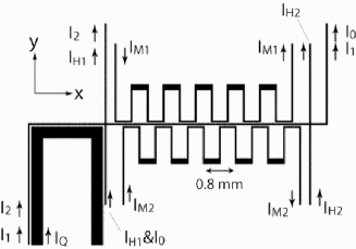
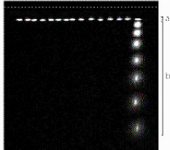
Our chip, depicted in figure 1, consists of two main sections. In the left section, the currents and can be used to create a large-volume quadrupole and Ioffe-Pritchard trap, respectively. In the right section with the meandering currents and , moving potential wells can be created to transport the trapped atoms. The two straight wires H1 and H2 to the left and to the right of the conveyor section can be used to create stationary magnetic traps and barriers.
2.1 Loading into the large-volume trap
For applications which require very cold or even Bose condensed atoms, a trap with a large initial volume is necessary, since typically of the atoms are lost in the course of evaporative cooling to BEC. We use a current in the U-shaped wire together with the offset field to create and compress a mirror-MOT of large volume (see figure 1). After polarization gradient cooling and optical pumping, an elongated Ioffe-Pritchard trap is created with A and a bias field G. In this trap, we capture up to atoms at a typical temperature of 45K. If lower temperatures are required, we perform radio-frequency induced evaporative cooling [7]. To achieve a high elastic collision rate, we compress the trap by ramping to 55 G within 300 ms. We then relax the trap by reducing the offset field to 40 G and, if needed, perform a second stage of evaporative cooling. Figure 2 describes the steps that transfer the atoms from this trap into the conveyor.
2.2 Direct loading into the conveyor belt
Alternatively, atoms can be loaded directly into the conveyor potential. In this case, quadrupole fields for the last MOT stage are created below the meandering wires as shown in figure 3. After polarization gradient cooling and optical pumping, the magnetic conveyor is switched on as detailed in the figure caption. The volume of these traps is comparatively small, such that loading at typical MOT densities limits the atom number to a few per well. Temperatures of 10 to 50 K and densities on the order of are obtained in this way.
3 Transport and nanopositioning
The atomic conveyor belt was proposed in [20] and first demonstrated in [9]. In its simplest implementation, sinusoidally modulated currents are used to displace the ‘bins’ containing the atoms. In this case, the bins follow an overall straight path with a superimposed periodic deviation, as described in [9]. Here we show how numerical optimization of the modulated currents and bias fields can be used to reduce the periodic deviation, such that ideal linear transport is approximated with micrometric accuracy. This optimization was crucial to achieve the goal of non-destructive BEC transport [7].
3.1 Basic conveyor belt
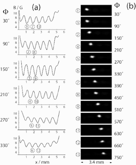
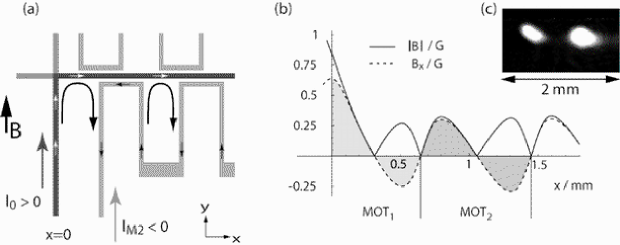
The conveyor belt consists of two main components (figure 1). A 2D-Ioffe-Pritchard potential is created by the current A and an external bias field G. This potential traps the atoms in the - plane. The confinement along is accomplished by the meandering currents and and an external bias field G. The resulting potential consists of a chain of minima as shown in figure 4. When the currents are modulated according to
| (1) |
these minima move continuously to the right with increasing phase angle In the experiment of figure 4, is varied linearly with time, with ms. We call this mode of operation the “basic conveyor belt”. Given the spatial period of m, the atoms are transported at a velocity of mm/s and traverse the full conveyor length of mm within 863 ms. At this velocity, we do not observe losses due to the transport, and the heating is below our temperature resolution of K.
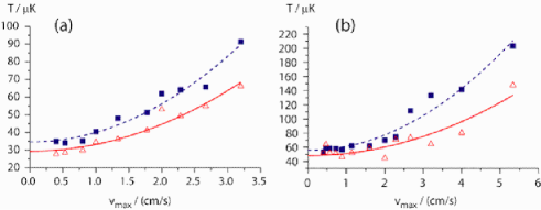
However, if we increase the transport velocity to more than , the atom cloud is measurably heated (figure 5). Two effects contribute to this heating: First, deviations of the trap position from the ideal straight line cause small periodic accelerations. Second, shape and steepness of the trap also vary periodically. Both heating effects can be reduced, or even completely avoided, by optimizing the time dependence of the various currents and bias fields. This is demonstrated in the next two subsections.
3.2 Height optimized version
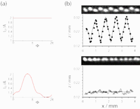
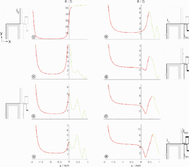
In the basic version of the conveyor discussed above, one obvious deviation from the ideal linear transport is the variation in height. The experiments and simulations in the upper row of figure 6 show that the excursions are of the order of m. This effect can be understood from figure 1: once per period, the potential minima pass through a position where both meandering wires are close to the central wire. This happens for , when both currents and are running antiparallel to the main current . The atoms then feel a smaller effective current along . Since the trap-surface distance is proportional to the atoms move closer to the wire at these positions. This vertical excursion can be avoided if the central current and/or the field are adjusted appropriately.
For our experiments, we have chosen to keep constant and to vary . A numerical optimization of has been used to keep the height of one particular well constant during one shifting period. The resulting current is plotted in figure 6 (a). The experimental results figure 6 (b) show that the height is indeed constant to m, even over the whole conveyor length.
Despite this optimization of the height, the heating rate at high transport velocities is only slightly reduced (figure 5). This is due to the fact that the deviation in the -direction has been left uncompensated. Furthermore, as mentioned above, the shape of the trapping potential changes significantly during the transport. This also appears in the variation of the axial and transverse trapping frequencies, and , which characterize the potential at the bottom of the trap. For very cold ensembles of atoms, the conveyor can be further optimized, as described in the next subsection.
3.3 Optimized BEC transport
When the atom cloud is so cold that it remains within the parabolic region of the potential, the task to keep the potential shape constant reduces to keeping the three trap frequencies constant. The two transverse frequencies are very similar and are mainly given by the 2D-Ioffe-Pritchard potential. Therefore, we can influence them by changing the current and the offset fields and . The axial frequency is due to the meandering currents and and can be adjusted by changing the amplitude of the currents. In a final step, we take into account that the trap position along is not an exactly linear function of .
For every , we have numerically calculated appropriate values of to obtain a trap at position , m with frequencies Hz and Hz. is coupled to and varies between 378 and 393 Hz over the full range of values. was not taken into account in the optimization because we cannot modulate in our current setup.
3.4 Positioning accuracy
An important application for the atomic conveyor belt is precise positioning of an atom (cloud) inside an optical resonator. For cavity-QED experiments, the atom-field coupling crucially depends on the overlap between the atomic wavefunction and the cavity mode. For these experiments as well as for scanning atomic microscopy [22], positioning accuracy of the trap center is essential. It is interesting to evaluate the position accuracy for a chip trap under realistic experimental conditions, i.e. in the presence of fluctuating fields, field gradients and currents. As a realistic example, we consider a trap with the highest transverse trapping frequency that we have achieved in our setup, which is 11 kHz. (Much higher frequencies are possible with straightforward technical improvements – see e.g. [4].) The parameters for this trap are A, A and G; the trap is located m from the chip surface. The transverse ground state extension ( radius) in this trap is 100 nm. The axial trapping frequency and the axial ground state extension are 730 Hz and 400 nm, respectively.
If we assume a relative current stability of in all current sources that are used to create the trapping fields, a simulation yields a position jitter of nm. Furthermore, the trap position is sensitive to fluctuating ambient magnetic fields in the -plane and to the component of an ambient magnetic field gradient. Their contribution to the displacement amounts to and . Ambient field stabilities of and can be reached with relatively small effort (in atomic fountain clocks, residual field fluctuations and gradients are several orders of magnitude smaller than this [23]). Therefore, an overall positioning accuracy of a few nm is certainly realistic. This is almost two orders of magnitude smaller than the trap’s ground state extension and more than two orders of magnitude smaller than the main optical transition wavelengths for Rb (nm and 795 nm). Thus, the assumed stability certainly suffices for applications which require a position accuracy in the range. Note that the position jitter from current fluctuations only affects the coordinate. For external field fluctuations below 0.2 mG, this is the main contribution to the overall position jitter – the position in the -plane is as stable as nm and nm.
3.5 Outlook
With this optimization, the conveyor belt can now be used for ultraprecise positioning of BECs and single atoms. This is closely related to the nanopositioning of single trapped ions that was used to map out the light field distribution in an optical cavity [24]. Indeed, we are currently using a two-layer variant of the conveyor belt [9] to position atoms in the evanescent optical field of a microsphere resonator for single-atom detection [25].
4 Double wells: Divide and unite
A double well potential with adjustable barrier height is the central building block for the proposed chip-based collisional phase gate [18] and trapped-atom interferometer [16, 17], but also for a magnetic technique [9] to continuously pump an atom laser by replenishing its atom reservoir [3], and for Josephson-type effects with BECs [26, 27, 28, 29].
Below we demonstrate two different current configurations that generate adjustable magnetic double wells. We use the first configuration to split and reunite a thermal cloud. By measuring the temperature after up to five iterations of this process, we show that it is adiabatic to very good approximation. With the second configuration, we split a BEC as was first done with optical fields in [30]. Although the well spacing in our implementation is still too large to observe interference fringes, this first on-chip BEC splitting provides important experimental input for future atom chip implementations of the phase gate and trapped-atom interferometer mentioned above.
4.1 Thermal cloud
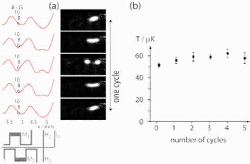
We first demonstrate the splitting and merging process with a thermal cloud positioned at the right end of the conveyor belt (figure 8). With the help of a time-dependent current in the additional wire H2, a stationary minimum is produced below that wire. Incoming minima from the left are merged with the stationary one if the current in H2 is driven according to A. All other parameters are controlled as described in section 3.1. The process was designed such that the left and the right wells have equal phase space volumes during the merging process. Reversing this process leads to the splitting of the trap. In figure 8 (b) the temperature of the merged cloud is plotted against the number of splitting and merging cycles. The temperature is essentially constant, indicating the adiabaticity of the process. The slight temperature increase presumably originates from a slight asymmetry in the splitting (). We attribute this asymmetry to an external field gradient along .
4.2 On-chip splitting of a BEC
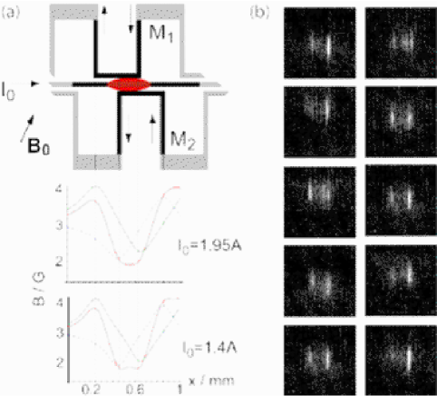
Fields on the conveyor chip can also be used to split a Bose-Einstein condensate. The atoms are transported to the position on the belt defined by (i.e., close to position 3 in figure 4). At this position, the single trap can be transformed into two traps by decreasing the trap–surface distance (figure 9). Simulations predict a symmetric splitting for mA and mA. In the experiment we found that the trap splits symmetrically with mA and mA. Again, this deviation presumably results from an external magnetic field gradient. With a constant external field G we split the initial single trap in two by decreasing the current from A to A within 50 ms. After splitting, the distance between trap centers is m and the barrier height is , corresponding to in our case. Each trap has a mean frequency Hz. For 1000 87Rb atoms in each trap, the chemical potential is In this configuration, tunnelling does not occur on relevant timescales. Figure 9 (b) shows 10 realizations of this experiment with identical parameters. These results show that symmetric splitting can be achieved on the chip; however, improved control over currents and external fields will be needed to obtain a reproducible splitting ratio. Also, in some images fringes are visible. These may originate from excitations or from phase fluctuations that occur just before splitting in the very elongated trap (cf. [31]). Using a more symmetric wire pattern [19] and magnetic shielding will lead to the improved stability that is a prerequisite for integrated atom interferometry and quantum information applications.
5 Cold atom dispenser
It is a specific advantage of the chip technology that complex devices can be obtained by combining simpler building blocks. Here we demonstrate a “cold atom dispenser” that combines the splitting, transport and merging functions described above. This device may enable the construction of a continuous atom laser [3] by purely micromagnetic means.
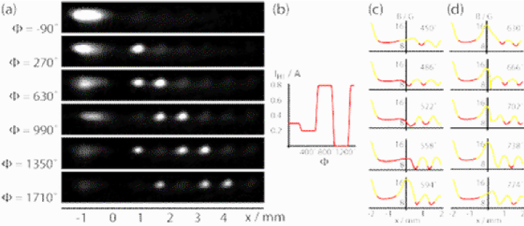
The dispenser is fed from a reservoir of trapped atoms to the left of the conveyor belt. This reservoir is produced by A, A, G and A (figure 1); the role of is to create an adjustable barrier between the reservoir and the conveyor. Switching on the conveyor belt with G does not extract any atoms from the reservoir yet; but if the current in H1 is decreased, atoms from the reservoir flood into departing conveyor belt bins. The fraction of atoms extracted from the reservoir depends on the height of the barrier. Figure 10 shows a reservoir containing atoms. We load the first two conveyor bins with atoms each by holding at 300 mA during the first and ramping it down to 200 mA during the second splitting (figure 10 (d)). (Since the atom number in the reservoir is smaller during the second splitting, has to be smaller in order to equal numbers of atoms into both bins). The third conveyor bin is left empty, which is accomplished by ramping to 800 mA, and the fourth conveyor bin is loaded again by ramping to 0.
In a third step, we were able to merge the partial clouds in a target trap at the end of the conveyor belt. This is shown in the video sequence Replenish (see sec. 6). A continuous atom laser based on this scheme would add an outcoupler to the target trap. The size of the reservoir needs to be improved for this application. Surface-induced evaporative cooling [20, 32] can be used to create a condensate in the reservoir, or even “on the fly” during transport on the conveyor. In this context, an interesting feature of the conveyor is that its transport direction can be curved [25]. In conjunction with pinholes, this can be used to protect the outcoupling region against laser light from the MOT in the loading region, and to establish a differential vacuum. The atom laser source would be pumped by the incoming condensates as demonstrated in [3].
6 Video sequences
To further illustrate the operation of the different devices we have created animated versions from series of absorption images. As our detection scheme is destructive, the trap is reloaded for each image and the temporal evolution of the parameters is rerun from the beginning to the time at which the atoms are to be imaged. Thus, the acquisition of a single image takes roughly 10 s, and a complete animation is recorded in 30 minutes or less, depending on the number of pictures. Computer control of the experiment and good stability of the setup enable automated acquisition of such movies.
The first three video sequences ConveyorBasic, ConveyorHoriz and BECConveyor show the different versions of the conveyor that we discuss in section 3.
The sequence Reunify illustrates the measurement in which the adiabaticity of the splitting process was demonstrated (cf. section 4.1). Splitting into more than two components is also possible and is shown in MultiSplit.
Two modes of operation of the atom dispenser (cf. section 10) are shown in the movies Replenish and SelectDeliv. In both versions, the consecutive separation of atom clouds has been complemented by replenishing the target reservoir at the end, as would be needed for the implementation of a continuous atom laser.
Additionally, we provide two further video sequences, which show the operation of two other on-chip devices that are closely related to those described above. For the movie Collider, two atom clouds were sent to the opposite ends of the conveyor. By suddenly switching off the currents in M1 and M2, the clouds are accelerated towards the trap center, where they penetrate each other. Since their initial density is only, less than of the atoms undergo a collision. With higher initial densities, this behaviour would change dramatically. This device is described in more detail in [19].
Finally, Sixty gives an example of a more complex atom trajectory in the plane perpendicular to the substrate. This kind of transport along a pre-defined trajectory is achieved by modulating wire currents and external fields according to functions that were obtained by numerical optimization. More details on this technique can be found in [33]. The example shown here was recorded on the occasion of the 60th birthday of one of the authors (TWH).
7 Conclusion
We have demonstrated atom chip devices that use time-dependent magnetic fields for atomic nanopositioning, splitting of thermal atomic clouds and BECs, and controlled atom dispensing. The potential use of these devices for atom chip-based quantum information processing, for atom interferometry with trapped atoms, for studies of Josephson effects and for pumping of atom lasers has been pointed out.
In order to realize the full potential of future atom chips, some important problems remain to be solved. In all the applications described here, trap-surface spacing was larger than m, so that surface-induced heating and losses [34] did not play a significant role. If, however, feature sizes approaching m are needed—as is the case for reasonably fast tunnel coupling between wells—the trap-surface distance will most likely also approach m, and surface effects can no longer be neglected [22]. High-resistivity materials [35, 32] and thinner conductor layers [34] may be a solution in many cases, especially as currents scale down with trap-surface distance. Corrugation of elongated potentials [36, 14] is currently an impediment for the realization of proposed guided-wave atom interferometers [37], but is likely to be remedied by improved manufacturing techniques [38, 39]. Devices with relatively strong confinement in all three dimensions, such as the trapped-atom interferometer [16], are generally much less affected by this problem.
Future atom chips will combine more and more functions on the same chip to achieve complex tasks. Thus, the next step towards a chip-based two-qubit gate would be to combine the magnetic double well with an electrostatic field [18, 40] or a microwave field [41] to obtain a state-dependent potential. Combination with optical fields generated by microoptical elements has also been proposed [42] and will further enhance the manipulation capabilities, in particular when trapping of all magnetic sublevels is required. Combining a conveyor belt with an optical resonator [25] offers exciting perspectives for single-atom detection and cavity QED with trapped atoms.
References
References
- [1] Greiner M, Mandel O, Esslinger T, Hänsch T W and Bloch I 2002 Nature 415 39
- [2] DiVincenzo D P 2000 Fortschritte der Physik 48 771
- [3] Chikkatur A P, Shin Y, Leanhardt A E, Kielpinski D, Tsikata E, Gustavson T L, Pritchard D E and Ketterle W 2002 Science 296 2193
- [4] Reichel J 2002 Appl. Phys. B 75 469
- [5] Folman R, Krüger P, Schmiedmayer J, Denschlag J and Henkel C 2002 Adv. At. Opt. Mol. Phys. 48 263
- [6] Ott H, Fortagh J, Schlotterbeck G, Grossmann A and Zimmermann C 2001 Phys. Rev. Lett. 87 230401
- [7] Hänsel W, Hommelhoff P, Hänsch T W and Reichel J 2001 Nature 413 498
- [8] Schneider S, Kasper A, vom Hagen C, Bartenstein M, Engeser B, Schumm T, Bar-Joseph I, Folman R, Feenstra L and Schmiedmayer J 2003 Phys. Rev. A 67 023612
- [9] Hänsel W, Reichel J, Hommelhoff P and Hänsch T W 2001 Phys. Rev. Lett. 86 608
- [10] Müller D, Anderson D Z, Grow R J, Schwindt P D D and Cornell E A 1999 Phys. Rev. Lett. 83 5194
- [11] Dekker N H, Lee C S, Lorent V, Thywissen J H, Smith S P, Drndić M, Westervelt R M and Prentiss M 2000 Phys. Rev. Lett. 84 1124
- [12] Cassettari D, Hessmo B, Folman R, Maier T and Schmiedmayer J 2000 Phys. Rev. Lett. 85 5483
- [13] Müller D, Cornell E A, Prevedelli M, Schwindt P D D, Wang Y J and Anderson D Z 2001 Phys. Rev. A 63 041602(R)
- [14] Leanhardt A, Chikkatur A, Kielpinski D, Shin Y, Gustavson T, Ketterle W and Pritchard D 2002 Phys. Rev. Lett. 89 040401
- [15] Hinds E A, Vale C J and Boshier M G 2001 Phys. Rev. Lett. 86 1462
- [16] Hänsel W, Reichel J, Hommelhoff P and Hänsch T W 2001 Phys. Rev. A 64 063607
- [17] Shin Y, Saba M, Pasquini T A, Ketterle W, Pritchard D E and Leanhardt A E 2004 Phys. Rev. Lett. 92 050405
- [18] Calarco T, Hinds E A, Jaksch D, Schmiedmayer J, Cirac J I and Zoller P 2000 Phys. Rev. A 61 022304
- [19] Reichel J, Hänsel W, Hommelhoff P and Hänsch T W 2001 Appl. Phys. B 72 81
- [20] Reichel J, Hänsel W and Hänsch T W 1999 Phys. Rev. Lett. 83 3398
- [21] Blackman R B and Tukey J W 1958 The Measurement of Power Spectra from the Point of View of Communications Engineering (New York: Dover Publications) p 98
- [22] Lin Y, Teper I, Chin C and Vuletic V 2004 Phys. Rev. Lett. 92 050404
- [23] Bize S, Sortais Y, Santos M S, Mandache C, Clairon A and Salomon C 1999 Europhys. Lett. 45 558
- [24] Guthöhrlein G, Keller M, Hayasaka K, Lange W and Walther H 2001 Nature 414 49
- [25] Long R, Steinmetz T, Hommelhoff P, Hänsel W, Hänsch T W and Reichel J 2003 Phil. Trans. R. Soc. Lond. A 361 1375
- [26] Giovanazzi S, Smerzi A and Fantoni S 2000 Phys. Rev. Lett. 84 4521
- [27] Williams J E 2001 Phys. Rev. A 64 013610
- [28] Menotti C, Anglin J R, Cirac J I and Zoller P 2001 Phys. Rev. A 63 023601
- [29] Pu H, Zhang W and Meystre P 2002 Phys. Rev. Lett. 89 090401
- [30] Andrews M R, Townsend C G, Miesner H J, Durfee D S, Kurn D M and Ketterle W 1997 Science 275 637
- [31] Dettmer S, Hellweg D, Ryytty P, Arlt J J, Ertmer W, Sengstock K, Petrov D S, Shlyapnikov G V, Kreutzmann H, Santos L and Lewenstein M 2001 Phys. Rev. Lett. 87 160406
- [32] Harber D, McGuirk J, Obrecht J and Cornell E 2003 J. Low Temp. Phys. 133 229
- [33] Reichel J and Hänsel W in Laser physics at the limits, eds. H Figger, D Meschede and C Zimmermann (Berlin Heidelberg New York: Springer, 2002) 471 – 475
- [34] Jones M P A, Vale C J, Sahagun D, Hall B V and Hinds E A 2003 Phys. Rev. Lett. 91 080401
- [35] Henkel C, Pötting S and Wilkens M 1999 Appl. Phys. B 69 379
- [36] Fortagh J, Ott H, Kraft S and Zimmermann C 2002 Phys. Rev. A 66 041604
- [37] Andersson E, Calarco T, Folman R, Andersson M, Hessmo B and Schmiedmayer J 2002 Phys. Rev. Lett. 88 100401
- [38] Wang D, Lukin M and Demler E 2004 Phys. Rev. Lett. 92 076802
- [39] Estève J, Aussibal C, Schumm T, Figl C, Mailly D, Bouchoule I, Westbrook C I and Aspect A 2004 Preprint physics/0403020
- [40] Krüger P, Luo X, Klein M W, Brugger K, Haase A, Wildermuth S, Groth S, Bar-Joseph I, Folman R and Schmiedmayer J 2003 Phys. Rev. Lett. 91 233201
- [41] Treutlein P, Hommelhoff P, Steinmetz T, Hänsch T W and Reichel J 2004 Phys. Rev. Lett. 92 103005
- [42] Birkl G, Buchkremer F B J, Dumke R and Ertmer W 2001 Optics Comm. 191 67