Quantum computation in optical lattices via global laser addressing
Abstract
A scheme for globally addressing a quantum computer is presented along with its realisation in an optical lattice setup of one, two or three dimensions. The required resources are mainly those necessary for performing quantum simulations of spin systems with optical lattices, circumventing the necessity for single qubit addressing. We present the control procedures, in terms of laser manipulations, required to realise universal quantum computation. Error avoidance with the help of the quantum Zeno effect is presented and a scheme for globally addressed error correction is given. The latter does not require measurements during the computation, facilitating its experimental implementation. As an illustrative example, the pulse sequence for the factorisation of the number fifteen is given.
I Introduction
Over the past few years, Benjamin Benjamin (2000, 2001, 2002); Benjamin and Bririd (2003), in particular, has followed up an initial proposal by Lloyd Lloyd (1993) on the concept of global control schemes for quantum computation. The motivation for such schemes is simple - instead of needing individual elements for the manipulation of every single qubit in a system, which is technologically very difficult, we control a very limited set of fields that are applied to all the qubits in the system. It is in this sense that we use the term ‘global addressing’ - we will use lasers with a beam width that addresses the whole ensemble of atoms. While every qubit will be given the same commands, we shall demonstrate the techniques that localise the effects so as to carry out operations on only single qubits.
Recently Calarco et al. (2004), a practical scheme has been proposed to implement such ideas with optical lattices (see also Vollbrecht et al. (2004)). Here we present another possible scheme, which has a number of advantages in terms of ease of implementation and especially scalability, where we can perform computation in two, or even three, dimensions of an optical lattice. As we shall see in the following, the present scheme gives the possibility to incorporate error correction and fault tolerance in a straightforward manner.
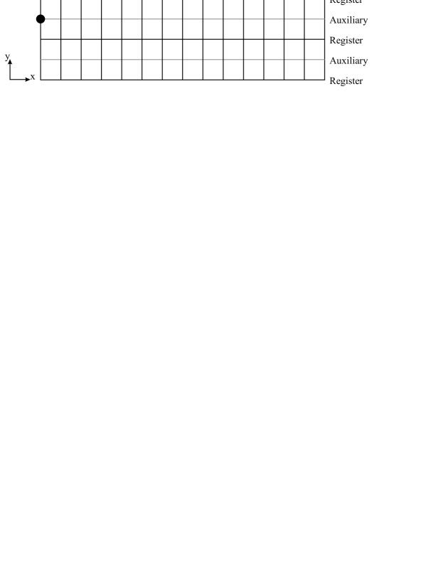
The way that we implement global control is relatively simple. We have a register array of qubits on which we wish to perform computation and an auxiliary array for which we retain single qubit control over a certain lattice site comment . This enables us to initialise a pointer (referred to as a control unit or marker atom in previous works) which is essentially a unique component which we can use to localise operations while applying global operations. Initially, the pointer is just the same atom as all other qubits, trapped in the lattice in the state , except that we individually rotate it to the state . By exclusively using global addressing, we can move this pointer atom relative to the computational qubits and apply controlled- operations which then effects solely on the qubit adjacent to the pointer. Two-qubit gates can be implemented in a similar way, using a three qubit gate such that, in the presence of the pointer, the desired gate is enacted on two neighbouring qubits. This control set is sufficient to give universal quantum computation. In comparison the schemes requiring individual addressing, the only additional resources are those required to move the pointer around the lattice structure. For a -dimensional structure of qubits, this will increase the total number of steps by a factor of order . Significantly, error avoiding and error correcting techniques can be implemented that respect the global addressing requirement and render our computational scheme favourable for scalable quantum computation.
II Atomic system and superlattices
II.1 Atomic system and optical lattices
An important tool in the manipulation of atomic ensembles is the employment of optical lattices. These can generate one, two or three dimensional structures of potential minima that can be used to trap atoms. In particular, consider two species of atoms, namely , that are confined within sinusoidal configurations of optical lattices produced by lasers of wavelength . These species can be two different internal ground states of the same atom, which can then be trapped and manipulated by two optical lattices of different polarisations. When the atoms are cold enough and the amplitudes of the optical lattices are sufficiently large, the atoms become restricted to the lowest Bloch-band. Hence, the evolution of the system can be described by the Bose-Hubbard Hamiltonian,
| (1) |
This is comprised of tunnelling transitions of atoms between neighbouring sites of the lattice,
| (2) |
and collisional interactions between atoms in the same site
| (3) |
where is the recoil energy, , is the mass of the atoms, is the potential barrier between neighbouring lattice sites and is the s-wave scattering length of the colliding atoms.
The collisional couplings can be arranged to take significantly large values via Feshbach resonances Inouye et al. (1998); Donley et al. (2001). Small tunnelling couplings, with respect to the collisional ones, can be produced by increasing the amplitude of the laser fields comprising the optical lattice. In this way, the system can be brought into the Mott insulator phase with only one atom per lattice site Kastberg et al. (1995); Raithel et al. (1998); Greiner et al. (2002a, b).
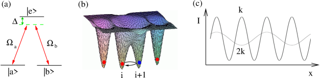
We encode the logical and of the computation in the and ground states of the atom, which correspond to the populations of the different modes of the optical lattice. As seen in Figure 1(a), the state of an atom can be transported between modes and by performing Raman transitions.
II.2 Simulation of spin Hamiltonian
We initially consider that the optical lattice system is brought into the Mott insulator regime where there is only one atom per lattice site. By manipulating the tunnelling couplings, it is possible to obtain a nontrivial evolution suitable for performing quantum computation. It is possible to expand the evolution due to the Bose-Hubbard Hamiltonian in terms of the small parameters . Up to second order in perturbation theory, this expansion is given, in terms of the Pauli matrices Kukov and Svistunov (90); Duan et al. (2003); Pachos and Rico (2004), by
| (4) |
The couplings are given by
Single particle phase rotations of the form can be cancelled with
The local field can then be arbitrarily tuned by applying appropriately detuned laser fields.
The effective couplings can be tuned by manipulating the amplitudes of the laser fields that generate the optical lattices. In particular, by activating only one of the two tunnelling couplings, e.g. , we can obtain the diagonal interaction along all the qubits of the lattice. This, up to local qubit rotations, is equivalent to a series of control phase gates (CP). However, if we activate both of the tunnelling couplings with appropriate magnitudes, it is possible to activate the exchange interaction . When applied for a sufficient time interval it results in a SWAP gate, exchanging the atoms at neighbouring lattices sites.
We have used an effective Hamiltonian to create the gates that we are interested in. The creation of these gates is studied in more detail in Pachos and Knight (2003), where the error introduced by the real Hamiltonian is examined for experimentally sensible parameters. Currently achievable errors are shown to be of the order of , which is small enough for an in–principle demonstration, even if it is not small compared to thresholds for fault tolerance Steane (1998). Ref. Pachos and Knight (2003) also shows how to create such gates without resorting to an effective Hamiltonian in the adiabatic regime, giving much shorter time scales for gate implementation.
II.3 Superlattices
As we have seen in the previous section, it is possible to control the tunnelling coupling constants by modifying the amplitude of the standing laser fields. The way to avoid single atom addressing is to employ “superlattices” (see Figure 1(c)), that is the superposition of optical lattices with different wavelengths. This will eventually be sufficient for performing universal quantum computation. With superlattices, we can manipulate the tunnelling couplings, , and consequently the effective couplings , by varying the potential barrier , as seen in equation (2). In particular, we shall employ two independent lattices whose spatial periods differ by a factor of two. This can be achieved, for example, with two pairs of laser beams, each one creating a lattice with period that depends on the angle between them Peile et al. (2003); Calarco et al. (2004). Hence, by choosing s appropriately, one can achieve a light-shift potential given by
| (5) |
where and is the phase difference between the second pair of lasers, while the first pair is taken to be in phase. By changing the amplitudes and the phase it is possible to obtain the control procedures necessary for the realisation of the presented scheme. In the same way, one can create the desired three dimensional lattice structures.
Raman transitions can be performed on every other qubit in a desired direction by employing similar structures of standing waves that are properly tuned, creating a two photon transition between the atomic ground states and . If we denote the laser Rabi frequencies that couple the states and by and respectively, then the coupling of the two states is given by . The excited state has a detuning of , as shown in Figure 1(a). By positioning the lasers such that the s have a sinusoidal configuration, we can activate the Raman transition only on alternate rows. We will commonly tune this to activate the transition on the register arrays without affecting the auxiliary ones.
III Quantum computation with superlattices
In what follows, we show how to perform one and two qubit gates between any qubits. To do this, we need to transport the pointer qubit to any desired location. In particular, for a single qubit gate we first transport the pointer next to the targeted qubit, . A conditional unitary transformation is then applied between the auxiliary array and the register one. This acts if the auxiliary qubit is in the state , resulting in a gate only on the qubit conditioned by the pointer. In order to perform a two qubit gate, we need to perform interactions between all three qubits, the two targeted ones, and , and the pointer.
In principle, there is much freedom in choosing the geometry for performing such steps. The minimal one dimensional case is rather cumbersome. Alternatively, one can use semi-one dimensional models, e.g. ladders, consisting of two parallel interacting arrays of qubits, one being the auxiliary array and the other the register. In terms of control procedures, the square configuration adopted here (see Figure 2) requires the least resources. The lattice comprises standing laser fields with wavelength which we assume are perpendicularly oriented. We prepare the qubits such that one is placed at each site of the lattice, all in the state . The pointer is then created by performing on one of these qubits. We consider that the register qubits are in arrays along the direction and occupy every other lattice array along the direction. At the same time, the auxiliary arrays between them are used for the transportation of the pointer qubit.
The idea is to use global laser addressing to perform all the necessary manipulations on the lattice to result in quantum computation on the register qubits. These manipulations, with their equivalent physical implementation, are described in the following.
III.1 Transport of pointer qubit along the same or different auxiliary arrays
The transport of the pointer qubit along an array can be performed by activating a lattice as given in Figure 3(a).
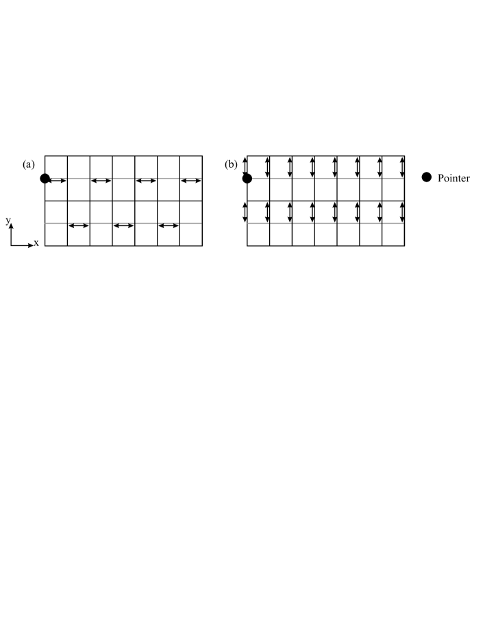
The superimposed lattices create minima between the pointer qubit and its appropriate neighbour on its left or right, resulting in the SWAP interaction between them. By exchanging the minima between neighbouring links, it is possible to move the pointer to any lattice site along the direction. To transport the pointer qubit to a different auxiliary array we have to superimpose the optical lattice given in Figure 3(b). This exchanges the auxiliary and the register arrays, resulting in the transport of the pointer along the direction. These techniques can be combined to transport the pointer to any location we want in order to perform a one qubit gate on the desired qubit. This manipulation also plays a significant role when performing two-qubit gates. If we implement this interaction on the register arrays, then qubits that are separated by an even number of lattice sites can be moved next to each other. Qubits that are separated by an odd number of sites do not move relative to each other with this swapping mechanism.
III.2 One-qubit gates with common addressing
To perform a one-qubit gate on a certain qubit, , let us first move the pointer next to it, by successive SWAP operations, as presented in the previous subsection. We then perform, by a Raman transition, the rotation on all the register qubits without affecting the auxiliary qubits. This is possible if we activate the Raman transition between the ground states and of the atom by two standing laser fields along the direction with periodicity , as illustrated in Figure 4.
Then we perform a control phase gate (CP) between the auxiliary and the register arrays. This is realised by similar standing laser fields to those presented in Figure 3(b). In contrast to the fields we used to SWAP the qubits, where we lowered the intensities for both modes, now we aim to activate the tunnelling of only one of the atomic species Pachos and Knight (2003) giving, effectively, a CP gate. This will only apply to , as the rest of the qubits, coupled to the states of the auxiliary qubits, will not be affected. Next, we apply the inverse rotation, , to all the register qubits using the same laser configuration as we did for the initial Raman transition. The overall effect will be that all the register qubits will return to their original state, while the targeted one will be rotated by , a one-qubit gate. Note that for the most general one-qubit gate, we should apply CP twice to give the evolution , where Nielsen and Chuang (2000). However, a universal set of gates can be achieved without needing to use this more general form.
III.3 Two-qubit gates with common addressing
In order to perform a two-qubit gate between two particular qubits, and , of the register, we move the qubits such that they neighbour the pointer. We have already specified how to do this if the qubits are separated by an even number of qubits. If not, then we have to move the pointer next to (or , whichever is more convenient) and perform a controlled-SWAP, causing the separation between and to be reduced by 1 site and then they can be moved together. The need to move the two qubits together is common to all quantum computing schemes that rely on short range interactions and so, in comparison, this procedure does not introduce any additional overhead.
By performing a three-qubit gate between , and the pointer, such as the controlled-controlled-NOT gate (C2NOT) we effectively obtain a two-qubit gate between the targeted qubits. This three qubit gate can be constructed out of globally applied single qubit rotations and two qubit gates, which we have already used to create a localised single qubit gate. A suitable algorithm is given in Figure 6. We also use this to implement the controlled-SWAP.

This is sufficient to create a 2-qubit gate between and provided they are in the same row (i.e. on the same register). To perform such a gate between two qubits on different rows, we first have to move the qubits so that they are within one column of each other. This may require a controlled-SWAP gate using the pointer. The pointer then performs a controlled-SWAP to bring onto the auxiliary array. We then move the auxiliary array such that it is adjacent to the register containing . We are then in a position to perform our gate, after which should be returned to its original position. The combination of all these procedures results in universal quantum computation for the two dimensional register, and can be trivially extended to three dimensions.
III.4 Qubit Measurement
The final step in performing quantum computation is a measurement stage. This can also be accomplished with the help of the pointer. We move the pointer so that it is on the same square, but diagonally opposite, the qubit we wish to measure, . We then perform the C2NOT procedure presented in the previous subsection, but rotated by . The effect of this is to entangle with the auxiliary qubit adjacent to the pointer, giving the state . If we then measure the auxiliary array using a standing wave with double the lattice period, then this will correctly measure , without affecting the register array (except for the one qubit that we measure).
Practically, there is a potential problem in implementing this idea with global addressing. When we perform a measurement as specified in Beige and Hegerfeldt (1997), we choose which state to measure, either or . If this state is occupied, then we are at risk of losing the atom from the optical lattice. Hence, we can’t measure the whole line of auxiliary qubits because we would lose the pointer. This problem can be avoided if we use a technique similar to that which we are using on the single-qubit gates, and only measure every other qubit on the auxiliary array.
III.5 Pointer Initialisation
Up to now, we have assumed that we can create a pointer on a single lattice site. Technically, this is not a straightforward procedure, hence the desire for global addressing. However, as a one-off effect, we can achieve a single qubit rotation. Recall that, before we create the pointer, the system consists of a lattice of qubits all in the state. The way in which we intend to create a pointer is to use a tightly focused laser to create a rotation on a single qubit. In general, this laser will not have a small enough Gaussian profile and it will create small rotations on neighbouring qubits. To circumvent this problem, one can impose a second lattice of double wavelength along both dimensions, as seen in Figure 7(a). This lattice should address the eight nearest neighbours to the qubit we wish to rotate, causing continuous measurements on their state and thus preventing population of this state through the quantum Zeno effect Beige and Hegerfeldt (1997, 1997). This is accomplished by applying an additional laser with amplitude that couples the state to an excited state which spontaneously emits photons at a rate . This is illustrated in Figure 7(b), where the unwanted Raman transition between and is also depicted. The efficiency of this scheme has been studied by a simulation of the evolution of the state of the atoms that neighbour the pointer. Figure 7(c) shows the results of this simulation, plotting the fidelity of keeping the population of the neighbours fixed in the state, , and the success rate, . The success rate is the probability that no photon emission occurs during the process. We have assumed that the laser has a width of . This proves that significant suppression takes place for physically sensible laser profiles, since the fidelity can be brought close to 1. If photons are emitted, then they can be measured and the initialisation process can be repeated. In principle, further lattices can be applied, if necessary, to suppress the effect on the next-nearest neighbours.
Vollbrecht et al., in Vollbrecht et al. (2004), introduce a potentially very interesting concept which generates pointer qubits from imperfections in the lattice (the globally addressed computation component of their paper is only of secondary nature). This idea not only creates pointers, but also removes any imperfections in the loading of atoms into the lattice. We can, in fact, incorporate the idea into our scheme as an alternative procedure for preparing the pointer. We would do this by following the scheme presented in Vollbrecht et al. (2004) until ready to perform the computation. At this point, we add two additional steps. These involve, firstly, performing a controlled-NOT operation as defined in their scheme, so that the qubit adjacent to the pointer is placed in the state. Secondly, we reject the pointer qubit, so that there is only one qubit in each lattice site, hence we have converted from their pointer into our pointer. However, the authors of this paper accept that the number of steps required for this preparation is currently very demanding from an experimental perspective. It also requires a different set of controls to those which we use in the rest of the computation. Both of these factors make it preferable to use quasi-single qubit addressing outlined above.
IV Physical implementation of superlattices
In order to perform the previously presented quantum gates we need to enable couplings on alternate rows and between alternate pairs. The required arrangement of lasers can be calculated by specifying the potential offset from the base trapping potential that we need to create across the 2D structure. Specifically, we need to ensure that the zero offsets appear exactly where we want no interactions to occur. For example, let us assume that we want to create interactions as shown in Figure 8(b), and that the vertices where the qubits are located are separated by a distance of . The potential offset, , that we require can thus be written as
| (6) |
This expression can be expanded to give a sum of sine terms. Each term has a period and a direction. The period, , specifies the angle between the pair of lasers that is required to create that term and is given by
This potential, illustrated in Figure 8(a), can be implemented by the combination of two independent pairs of lasers, each one producing a potential offset, , given by
| (7) |
For example, taking the term , the required laser field has a wave vector along the direction of and a period . As a result, we can employ lasers of the same wavelength as those creating the trapping potential, where the doubling of the wavelength is produced by having . Similar setups can be used for generating the other control procedures of the previous section.
As a final point we would like to consider the influence of the superlattices on the harmonicity of the trapping potentials of the atoms. Around the potential minima, the superposition effect can be given by expansions of sine or cosine functions. The qubits that remain uncoupled get only even powers in the expansion including quadratic terms, and hence the location of the qubits remain unchanged. However, the qubits that become coupled obtain an term, and hence the trapping minima for the coupled qubits actually move together. This is not a problem provided the offset potential remains small compared to the trapping potential, and the superlattices are turned on adiabatically so the atoms remain in their ground states of the trapping potential. This also demonstrates that the trapping frequencies of the interacting qubits remain unchanged when the additional lattice field is introduced.
V Proposal for the experimental realisation of factoring 15
The standard experimental demonstration of a quantum computation is to factor 15 Vandersypen et al. (2001), the smallest meaningful factorisation, since the method fails for even numbers and powers of primes. The employed algorithms include a significant element of simplification (for a full description of such methods, see Vandersypen et al. (2001); Beckman et al. (1996)). Since we can already factor 15 by classically calculating all the steps in the algorithm, we can quickly realise that most of the work is redundant, enabling us to reduce the required control steps. This won’t be possible when we consider factoring much larger numbers.
The general factoring scheme, for a number , which is bits long, consists of taking qubits (the first register), and applying the Hadamard to each of the qubits. This creates an equally weighted superposition of all numbers, , from 0 to . We then take another qubits (the second register) and calculate , thus entangling them with the first register. is a number that is randomly selected from the numbers smaller than which satisfies . So, for , . This calculation will, in general, also require some ancillas to act as scratch space for the calculation. The next step is to apply the inverse Fourier transform on the first register and then measure these qubits. The result is used as the input to a classical continued fractions algorithm, which will finally yield one of the factors of .
We start the simplification process by noting that, in the case of , for all . This means that only the 2 least significant bits of affect the calculation on the second register. Furthermore, if we ‘randomly’ select (say), we find that and hence only the least significant bit of the first register matters. The computation that we have to perform then becomes very simple, while still creating the state

The more standard case to demonstrate is the choice of , where we have to act on 2 of the bits of . The circuit diagram for this is given in Figure 9 Vandersypen et al. (2001). In Table 9(b) we give the set of commands required to perform this factorisation, with the notation being defined in Figure 8(b).
The minimum device size is a grid of qubits. In general, the size of the optical lattice for computing on qubits needs to be qubits. The need for this can be seen in Figure 8(b) since if we were to apply , qubits and would try to move into empty lattice sites if the device size was just , but the interaction has different effects if those lattice sites are empty.
VI Error avoidance and error correction
VI.1 The Auxiliary Qubits
As with any proposal for quantum computation, decoherence is a significant issue that cannot be neglected. In a global control scheme, its significance only gets amplified. Such a scheme necessarily introduces more computational steps and so the algorithm will take longer to run, thus increasing the build-up of errors. Even more demanding is the requirement that our pointer qubit and, in fact, all the other qubits in the auxiliary array, are error free. If an error occurs in the auxiliary array, it will affect every gate throughout the rest of the computation.
Such an error would be catastrophic for our computation, and needs to be prevented. This can be achieved by noting that all the qubits of the auxiliary array are in classical states. These classical states are eigenstates of , and are thus unaffected by phase-flip errors. The effect of bit-flip errors can be reduced by using the quantum Zeno effect Beige and Hegerfeldt (1997). In principle, by continuous measurement, the probability of a bit-flip can be reduced to zero. Since all errors can be described in terms of phase flips, bit flips or a combination of the two, this renders the auxiliary array error free.
While applying the quantum Zeno effect we do not wish to lose the pointer during the measuring procedure. Consequently, we have to employ the same optical lattice that only measures every other qubit on the auxiliary array. This also means that we can never measure the state of the pointer. We have to use the measurement result of the other qubits to indicate how likely it is that an error has occurred on the pointer. If some of the auxiliary qubits are found in the state, then we have to consider it likely that the pointer has also been affected and stop the computation. In the following subsection, we present how error correction can be performed on the register qubits. In principle, similar concepts can be applied to the pointer. However, our current method requires significant modification of the physical models, and is in need of optimisation. This is an avenue for future study.
VI.2 The Register Qubits
Recent work Benjamin and Bririd (2003) has shown that error correction can be implemented on globally controlled quantum computers, and that the architecture even supports fault tolerance. The basic idea is that the qubits are divided up into blocks of qubits. These qubits will constitute one encoded qubit for error correction. A typical error correction phase of a computation involves extracting a syndrome measurement from the encoded qubits, thus finding out what errors have occurred and, depending on the results held on ancillas, correcting for the error. The way one can implement this in a globally controlled structure is to add extra quantum gates that feed back from the ancillas to correct for the errors, without ever actually measuring them. We also require a ‘switching station’, which is a classical pattern of qubits, for every encoded block of qubits. This switching station allows us to switch on and off pointers with the correct sequence of global pulses. The patterning required for error correction is simply a for one of the blocks, and a for all the others, as in Figure 10.
If we start with a pointer every qubits (and we will select to be even for the sake of the quantum Zeno effect, as described above), then the pointers start off with the correct parallelism for error correction. To switch to a phase where we want to apply operations to a single qubit, we just perform a controlled-operation using the switching station as the control.
There are several drawbacks with this implementation of error correction. The first is that such algorithms are currently outside experimental feasibility because they require several thousand steps (Benjamin and Bririd (2003) gives specifications for two common codes), which would require a longer time to perform than current decoherence times. The second is that these switching stations are susceptible to errors. We will have similar problems applying the quantum Zeno effect to them as we do to the auxiliary qubits. Finally, we have to take care of the ancillas. At the start of each error correcting phase, we require our ancillas to be in the state. At the end of this phase, they will contain an unknown error syndrome. These qubits either have to be reset, or replaced by fresh ancillas. In the discussion of 3D structure in the following section, we will present how the third dimension could be used to provide a significant supply of fresh ancillas. This greatly simplifies the experimental implementation of quantum error correction algorithms.
VII Proposed computational schemes and conclusions
There are many different ways that our scheme can be used for performing quantum computation with three dimensional optical lattices. The choice of which one should be used can be determined by setting different priorities, such as efficiency of scaling, signal sizes etc. We outline some of the possible uses below.
The conceptually simplest model is to arrange the computation on a one dimensional ladder, consisting of qubits on a single register array and a single auxiliary array, also consisting of qubits. This could be repeated across the whole three dimensional structure, so we would have approximately identical copies, all running in parallel. This is the least scalable architecture, since qubits are separated by steps. However, it is very useful in terms of signal strength when we make a measurement at the end of the computation. Using the computer with many copies running in parallel gives an ensemble computation, where expectation values of the computational result can be given at the end. Alternatively, we can perform computation on a two dimensional grid by moving the registers relative to the auxiliaries with a series of SWAPs in the direction. All qubits are within steps of each other, and so the structure scales more easily. We could also get a reasonable signal strength due to the parallel planes in the third dimension. As a final alternative, we could perform computation on a single plane, leaving all the other planes in the state, kept there possibly by the quantum Zeno effect. These other planes can then be used for ancillas in the error correction phase. They can be easily accessed as the computational plane can be moved through the other planes in the same way that the auxiliary array can be moved past the register arrays.
Naturally, other possible arrangements exist, but these three illustrate some of the simple ideas that can be used. It is also important to remember that we are free to rearrange the labelling of our qubits so as to minimise the path of the pointer. Some operations can also be reorganised to minimise its path. These procedures can have a significant effect on the number of steps required to implement an algorithm, and hence also on the errors, and the practicality. Such an example has been given in a previous section where a convenient arrangement was given for the implementation of factoring 15. The significant remaining issue is the number of gates that can be implemented within the system’s decoherence time.
Our scheme has significant differences in comparison to those already proposed Calarco et al. (2004); Vollbrecht et al. (2004). At the most fundamental level, we interact qubits in a different way, making use of the tunnelling interaction Pachos and Knight (2003) instead of collisional couplings Mandel et al. (2003). These are just two different experimental techniques and the current state of the art provides little to pick between them for performing global addressing quantum computation. The collisional schemes, however, have significant complications and/or drawbacks. Both these schemes use an additional qubit whose presence, or lack thereof, is crucial in performing quantum gates. This gives the pointer a very special position. In the present proposal, the pointer is not that special, it is just the same as every other qubit, experiencing the same fields etc. This makes experimental realisation easier, but also contributes to the complexity of the ideas required for the scheme. The work of Calarco et al. (2004) has significant issues associated with the initialisation procedure. They require a filling of one qubit on every other lattice site, which has been experimentally demonstrated in Peile et al. (2003). However, the pointer (referred to as a marker atom) is an extra atom that has to be inserted into one of the gaps.
Our proposal extends the work presented in these papers by including control sequences that are particularly suitable for global addressing and it incorporates the concepts of error correction and avoidance Benjamin and Bririd (2003). It is unclear as to whether the scheme in Vollbrecht et al. (2004) could be generalised to give the regular patterns required for error correction and fault tolerance, whereas the pointers in our proposal have no special place and can easily be prepared once a single pointer has been initialised.
Acknowledgements.
This work was supported by EPSRC and a Royal Society URF.References
- Benjamin (2000) S. C. Benjamin, Phys Rev A 61, 020301 (2000).
- Benjamin (2001) S. Benjamin (2001), quant-ph/0104117.
- Benjamin (2002) S. C. Benjamin, Phys. Rev. Lett. 88, 017904 (2002).
- Benjamin and Bririd (2003) S. C. Benjamin and A. Bririd (2003), quant-ph/0308113 .
- Lloyd (1993) S. Lloyd, Science 261, 1569 (1993).
- Calarco et al. (2004) T. Calarco, U. Dorner, P. Julienne, C. Williams, and P. Zoller (2004), quant-ph/0403197.
- Vollbrecht et al. (2004) K. Vollbrecht, E. Solano, and J. I. Cirac (2004), quant-ph/0405014.
- (8) We shall later demonstrate how this can be done in practice.
- Inouye et al. (1998) S. Inouye, M. R. Andrews, J. Stenger, H.-J. Miesner, D. M. Stamper-Kurn, and W. Ketterle, Nature 392, 151 (1998).
- Donley et al. (2001) E. A. Donley, N. R. Claussen, S. L. Cornish, J. L. Roberts, E. A. Cornell, and C. E. Wieman, Nature 412, 295 (2001).
- Kastberg et al. (1995) A. Kastberg, W. D. Phillips, S. L. Rolston, and R. J. C. Spreeuw, Phys. Rev. Lett. 74, 1542 (1995).
- Raithel et al. (1998) G. Raithel, W. D. Phillips, and S. L. Rolston, Phys. Rev. Lett. 81, 3615 (1998).
- Greiner et al. (2002a) M. Greiner, O. Mandel, T. Esslinger, T. W. Hänsch, and I. Bloch, Nature 415, 39 (2002a).
- Greiner et al. (2002b) M. Greiner, O. Mandel, T. W. Hänsch, and I. Bloch, Nature 419, 51 (2002b).
- Kukov and Svistunov (90) A. B. Kukov and B. V. Svistunov (90), phys. Rev. Lett.
- Duan et al. (2003) L. M. Duan, E. Demler, and M. D. Lukin, Phys. Rev. Lett. 91, 090402 (2003).
- Pachos and Rico (2004) J. K. Pachos and E. Rico (2004), quant-ph/0404048.
- Pachos and Knight (2003) J. K. Pachos and P. L. Knight, Phys. Rev. Lett. 91, 107902 (2003), quant-ph/0301084.
- Steane (1998) A. Steane (1998), quant-ph/9809054.
- Peile et al. (2003) S. Peile, J. V. Porto, B. Laburthe, J. M. Obrecht, B. E. King, M. Subbotin, S. L. Rolston, and W. D. Phillips, Phys. Rev. A 67, 051603 (2003).
- Nielsen and Chuang (2000) M. A. Nielsen and I. L. Chuang, Quantum Computation and Quantum Information (CUP, 2000), 5th ed.
- Beige and Hegerfeldt (1997) A. Beige and G. C. Hegerfeldt, J. Mod. Opt. 44, 345 (1997).
- Beige and Hegerfeldt (1997) A. Beige and G. C. Hegerfeldt, Phys. Rev. A 53, 53 (1997).
- Vandersypen et al. (2001) L. Vandersypen, M. Steffen, G. Breyta, C. Yannoni, M. Sherwood, and I. Chuang, Nature 414, 883 (2001).
- Beckman et al. (1996) D. Beckman, A. Chari, S. Devabhaktuni, and J. Preskill, Phys. Rev. A 54, 1034 (1996).
- Mandel et al. (2003) O. Mandel, M. Greiner, A. Widera, T. Rom, T. Hänsch, and I. Bloch, Nature 425, 937 (2003).