Also at] Institute of Physics, National Center for Sciences and Technology, 1 Mac Dinh Chi Street, District 1, Ho Chi Minh city, Vietnam.
Efficiency of tunable band-gap structures for single-photon emission
Abstract
The efficiency of recently proposed single-photon emitting sources based on tunable planar band-gap structures is examined. The analysis is based on the study of the total and “radiative” decay rates, the expectation value of emitted radiation energy and its collimating cone. It is shown that the scheme operating in the frequency range near the defect resonance of a defect band-gap structure is more efficient than the one operating near the band edge of a perfect band-gap structure.
pacs:
42.50.-p, 42.70.Qs, 42.50.Dv, 03.67.DdI Introduction
There has been a fast growing interest in light sources that produce individual photons on demand, motivated, e.g., by potential applications in secure quantum key distribution Bennet84 and scalable quantum computation with linear optics Knill01 . Such sources would also be valuable in interferometric quantum nondemolition measurements Kok02 and as standards for light detection Barnes02 . Different applications of course impose different requirements on single-photon sources. For example, quantum indistinguishability of the photons is not necessary for quantum key distribution. On the other hand, photons that are indistinguishable and thus can produce multiphoton interferences are needed for quantum computation schemes with linear optical elements in general Santori02 . Any realistic source will be a result of trade-off among different, sometimes conflicting requirements. For example, an improvement of the timing of the generation of the photons will broaden their spectral profile.
Search for realizable single-photon sources has been widespread, with the schemes ranging from attenuated laser pulses and parametric down-conversion to single emitters, and numerous strategies have been explored in order to enhance the performance of the sources. Faint laser sources provide well-collimated narrow-band outputs but suffer from the Poissonian statistics, i.e., the possibility of letting more than one photon being emitted during a single shot. Parametric down-conversion produces a pair of photons at a time, allowing one photon to herald the existence of the other one. Due to the constraint of phase matching, it is possible to know the output trajectory, polarization and wavelength of the heralded photon. However, the scheme raises a couple of problems. Although the use of pulsed pumps restricts the pair emission time to a known interval, the actual moment of emission cannot be chosen on demand, because the conversion is a random process. Moreover, there is always the possibility of producing more than one pair of photons. To overcome the problem of multiple-photon emission while maintaining a high likelihood that one pair of photons is generated, a multiplexed system consisting of multiple down-converters and detectors has been suggested, such that it is highly probable that one photon pair is created somewhere in the array even at low pump intensities Migdall02 . The problem of random production might be mitigated with the aid of a storage scheme, where once a photon pair has been produced, the heralding photon activates a high-speed electrooptic switch that reroutes the other photon into a storage loop. The stored photon keeps circulating in the loop until being switched out at a later time chosen by the user Pittman02 . The most promising strategy to improve the performance of single emitter sources seems to be enclosing the emitter in a microcavity. The Purcell effect can then be exploited to shorten the lifetime of the excited emitter, thereby narrowing the time window during which the photon is emitted. Additionally, if the photon is most probably emitted into the fundamental mode of the cavity, which is often well-directed in space, unwanted omni-directional emission can be suppressed, thereby increasing the outcoupling efficiency Barnes02 .
To go a further step towards a deterministic single photon source, enclosing of a single emitter within a tunable planar photonic band-gap structure has been suggested Scheel02 . The transition frequency of the excited emitter is first inside the band gap near its edge, thus being prevented from the spontaneous decay. By exposing the solid backbone of the photonic crystal to a short optical pulse, the band gap is then shifted, e.g., due to the Kerr nonlinearity, in such a way that the emitter transition frequency now falls in a region of high density of states. The emitter is at once forced to decay rapidly, releasing a photon. Unfortunately, the scheme cannot work efficiently, because the key element, namely, the assumed high contrast between the densities of states inside and outside the band gap (in the vicinity of the band edge) is an artifact of the one-dimensional theory Ho03 .
As has been shown recently Ho03 , a substantial contrast can be realized, if not a perfect photonic crystal is used but a photonic crystal containing a defect, with the working frequency range being the range around the defect resonance instead of that around the band edge. To gain first insight, in Ref. Ho03 only the total decay rate of the excited emitter has been studied. Clearly, this quantity cannot be regarded, in general, as a comprehensive measure of efficiency of the light source, because the decay of the excited emitter can be effectively nonradiative or the photon is emitted into an unwanted direction. In this paper, we give a more detailed assessment of the performance of the schemes, by investigating the expectation value of the emitted radiation energy, its angular distribution, and the “radiative” decay rate. We shall employ a quantum mechanical approach that allows one to fully take into account absorption and dispersion of the material media.
II Basic formulas
II.1 Poynting vector and energy flow through a surface
Let us begin with introducing the expectation value of the slowly varying Poynting vector of the quantized electromagnetic field Loudon03 ; Janowicz03
| (1) |
Here, means the quantum mechanical expectation value, and and are the positive (negative) frequency parts of the electric and magnetic fields, respectively,
| (2) | |||
| (3) |
where
| (4) |
Further, let
| (5) |
be the decomposition of the electric field in the free-field part and the source-field part, with the free-field part being in the vacuum state,
| (6) |
In particular, in the far-zone limit , with being an effectively real (positive) permittivity, the relation
| (7) |
is valid (, unit vector in the direction of ), and it is not difficult to show that in the far-field zone the relationship
| (8) |
holds, where the expectation value
| (9) |
is commonly referred to as the field intensity. Note that Eq. (8) is in agreement with Eq. (55) in Ref. Sondergaard01 .
The expectation value of the radiation energy transported through an area can be expressed in terms of the Poynting vector as
| (10) |
In particular, when the area is the surface of a sphere in the far-field zone,
| (11) |
then substitution of Eq. (8) into Eq. (10) leads to
| (12) |
where
| (13) |
is the expectation value of the radiation energy emitted per unit solid angle Ho00 . For a planar geometry, a surface of the form of a plane is clearly more appropriate. For a plane parallel to the -plane,
| (14) |
(, unit vector in the positive direction), from Eqs. (8) and (10) we obtain
| (15) |
where, in contrast to Eq. (12), the upper limit of the -integral is now .
II.2 Spontaneous decay
Consider a single emitter being placed at position and having transition frequency and (real) transition dipole moment . Various experimental realizations of single emitters have been considered (see, e.g., Refs. Barnes02 ; Ho03 and references therein). Here we do not assert very specific assumptions on the emitter except that the emission is the result of a spontaneous electric dipole transition, which implies that the size of the emitter is small compared to the radiation wavelength. Very importantly, the dipole emitter is surrounded by (linear) macroscopic bodies, which can be dispersing and absorbing and of arbitrary geometry.
Basing on quantization of the electromagnetic field in causal linear media, one can show that the spontaneous decay rate of an electric dipole emitter can be determined according to the formula Ho00 ; Agarwal75
| (16) |
where is the classical Green tensor of the medium-assisted Maxwell-field characterizing the surrounding media. Note that the atomic transition frequency already incorporates the medium-induced level shifts. The intensity of the spontaneously emitted light registered at some position (not necessarily in the far-field zone) and time reads Ho00
| (17) |
and the Poynting vector can be shown to be (App. A)
| (18) | |||||
Note that transit-time effects have been disregarded in Eqs. (17) and (18).
It is worth noting that Eqs. (16)–(18) apply to arbitrary geometry of the dispersing and absorbing bodies surrounding the dipole emitter. With the help of Eqs. (10) and (18) the radiation energy transported through an area located at any distance from the radiation emitting source can be calculated. In particular, when the area of interest is in the far zone, then the energy passing the area can be related to the field intensity through the relationship (8) and formulas such as (12) and (15) can be used.
II.3 Spontaneous emission in a planar structure
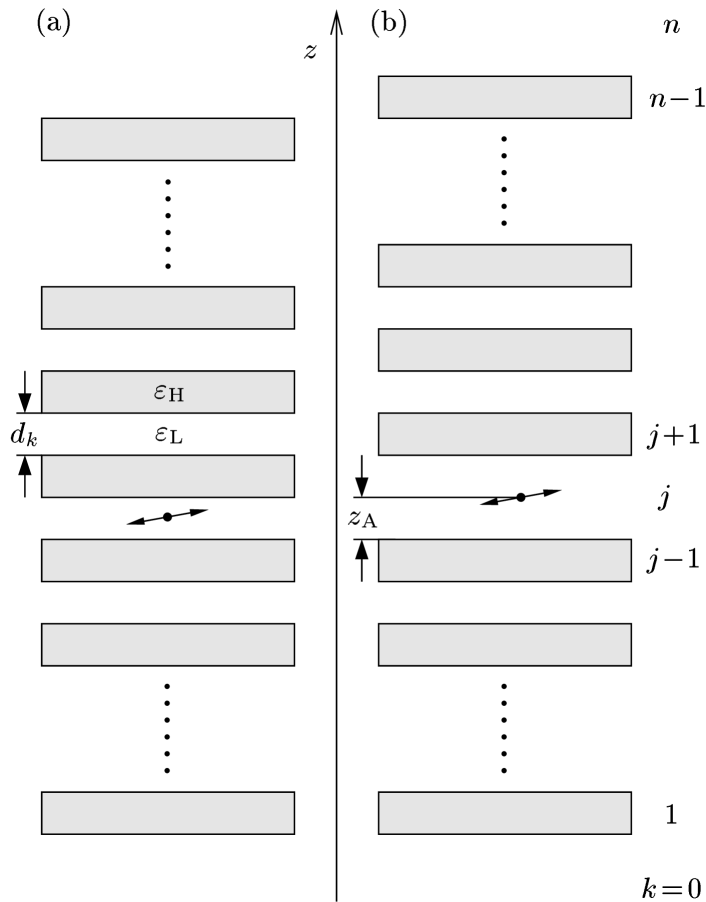
Let us consider a single (electric) dipole emitter sandwiched between two distributed Bragg reflectors as sketched in Fig. 1. The Bragg reflectors consist of plates of thickness of infinite lateral extension and periodically interchanging low and high complex permittivities and in direction. The zeroth and th “layers” represent the surrounding of the device. It is assumed that the th layer ( ) contains the emitter. If the thickness of the th layer is also , a band-gap structure is obtained; if it is the structure can be regarded as a planar photonic crystal with a defect or, equivalently, as a Fabry-Perot cavity whose mirrors are formed by distributed Bragg reflectors.
For simplicity we shall identify the Green tensor in Eqs. (16)–(18) with the unperturbed Green tensor for a planar multilayer, thereby disregarding local-field corrections. That is to say, should be real and close to unity [ ]. The Green tensor for a planar multilayer is well known and can be taken from Ref. Tomas95 . Substituting its imaginary part in the coincidence limit into Eq. (16), we obtain Ho03
| (19) |
[ , in-plane component of the wave vector], where
| (20) | |||||
with
| (21) | |||
| (22) | |||
| (23) |
and is the well-known decay rate in free space. Further, are the total reflection coefficients at the upper (lower) stack of layers, where and refer to TM and TE polarized waves, respectively.
Equation (19) together with Eq. (20) represents the total decay rate of the emitter, including the contributions from the “nonradiative” decay caused by material absorption and from the unwanted laterally guided radiation. To facilitate the determination of the “radiative” decay rate that is related to the radiation observable outside the device, the bulk and scattering parts of the Green tensor are, in contrast to Ref. Ho03 , not separated from each other, because both contribute to . Note that the bulk part of the Green tensor can be singled out by setting in Eqs. (II.3) and (23).
Let us assume that the surrounding area of the device is vacuum or an effectively nonabsorbing medium, i.e., [ ] can be regarded as being real. Then the radiation that can be collected outside the device (though not in their entirety because of the finite aperture of the collection optics) results from waves with ( ), because only for these waves ( ) is real. Thus, the rate related to the emission of these waves can be obtained according Eq. (19), by restricting the upper limit of the integral to ( ),
| (24) |
The ratio may be regarded, at least for weak absorption, as one of the measures of efficiency of the device. It is, in a sense, an estimation of the weight of the decay channel associated with the emission of radiation that can leave the device in principle. However, it comprises the radiation on the two sides of the device.
A quantity that clearly distinguishes between the two sides and accounts for the radiation that really escapes from the device on the wanted side is the expectation value of the radiation energy transported through a distant area on this side, as defined by Eq. (10). Let us choose a plane above the device in Fig. 1 as the area, so that Eq. (15) applies. The relevant Green tensor now reads Tomas95
| (25) |
where
| (26) | |||
| (27) | |||
| (28) | |||
| (29) |
[ , ; , ; , unit vector in direction; , generalized transmission coefficients]. For real and within the stationary phase approximation, Eq. (25) approaches Mandel95
| (30) |
as .
Now we can calculate the expectation value of the radiation energy emitted per unit solid angle, , by substituting in Eq. (17) for the Green tensor the far-field expression given by Eq. (30) and inserting the resulting expression for in Eq. (13). Integrating with respect to the polar angle over the -interval,
| (31) |
after some calculation we obtain
| (32) |
where
| (33) |
Note that when the transition dipole moment is normal to the area, parallel to the area, or completely random, then the relation is valid, because of the symmetry of the system with respect to . Finally, from the quantity , which is the amount of energy emitted per unit azimuthal angle , the total amount of energy passing an area sufficiently far above the device is obtained by further integration [cf. Eq. (15)],
| (34) |
From Eq. (32) it is seen that, as expected, only the components of the transition dipole moment in the -plane contribute to the far field observed in the normal direction ( ). Note that in free space, where
| (35) |
is valid, Eq. (34) simply yields
| (36) |
as it should be.
So far we have considered the case in which the detection area is above the device in Fig. 1. Clearly, Eqs. (32) and (34) also apply to the case in which the detection area is below the device, provided that is replaced with and is replaced with
| (37) |
Needless to say that is now understood as the angle between and the negative axis.
It should be mentioned that the angular distribution of the radiation energy of an oscillating classical dipole is described by formulas that are quite similar to the formulas given above and differ from them only in some factors. In particular, they have been used to investigate light scattering in planar three-layer structures Tomas95 and to study the efficiency of organic microcavity light emitting diode structures Wasey00 , with strongly absorbing metallic mirrors being taken into account. Since spontaneous decay is basically a pure quantum effect that has no classical analog, its consistent description should be based on quantum theory, without borrowing from elsewhere.
III Numerical results
The formulas derived in Sec. II.3 for the “radiative” decay rate and the expectation value of the emitted radiation energy are valid for any planar multilayer structure for which and is real. In the numerical calculations we have set and assumed that can be modeled by a single-resonance permittivity of Drude-Lorentz type according to
| (38) |
where corresponds to the coupling constant, and and are respectively the transverse resonance frequency of the medium and the linewidth of the associated absorption line.


The dependence on the transition frequency of the expectation value of the radiation energy emitted into the half space above the device in Fig. 1 is illustrated in Figs. 2 and 3 for a single dipole emitter in a planar band-gap structure (a) without and (b) with a defect layer. As expected, the radiation energy emitted there responds more sensitively to the band-gap structure in the case in which the transition dipole moment is parallel to the layers ( , ; Fig. 2) than in the case in which it is perpendicular to the layers ( , ; Fig. 3). It is further seen that the value of can substantially increase, particularly with regard to transition frequencies , with the number of periods in the bottom stack of layers of the band-gap structure containing the defect layer. The result clearly shows that highly unbalanced band-gap structures with the emitter being embedded in an appropriately chosen defect element are best suitable for realizing a large amount of radiation in the wanted space domain, which greatly helps to collect an emitted photon. Since photon emission in lateral directions and absorption of the emitted photon by the material cannot be completely suppressed, the upper limits and for a balanced scheme and an unbalanced scheme, respectively, are not reached. Note that unbalanced band-gap structures with defects are actually employed in experimental implementations of single-photon sources based on micropost microcavities (see, e.g., Ref. Santori02 and references therein).
The inset in Fig. 2 points up the effect that when the transition frequency is adjacent to the resonance frequency of the defect layer, then the emission can be switched from being (nearly) suppressed to being enhanced, by tuning of the permittivity of the band-gap material [here: ]. For the data in the figure, the appropriate frequency interval is , where the change of is about of . On the contrary, the change of achievable near the band edge of the band-gap structure without the defect layer is much less, viz at . The result is in full agreement with earlier conclusion drawn from an analysis of the total decay rate Ho03 .

Figure 4 illustrates the effect of material absorption on the emitted radiation energy . As expected, is seen to decrease with increasing . For the data in the figure, a noticeable effect is only observed for the band-gap structure with the defect layer above the working frequency . Clearly, the situation would change if one of the mirrors were made of metal, which features a much stronger absorption.
From Fig. 5 it can be seen that, as expected, for a balanced device the rate defined by Eq. (24) (for parallel orientation of the transition dipole moment) is a quite reasonable measure of the efficiency (compare the corresponding curves in Figs. 5 and 2). Though its frequency response is qualitatively the same as that of the total decay rate , the values of the two rates can substantially differ from each other. It is worth noting that the frequency response of and the frequency response of (solid curves in Fig. 2) agree almost completely for the chosen (small) value of the absorption parameter . To elucidate this agreement, we change in the integral in Eq. (34) [together with Eq. (32)] the integration variable according to . Thus we may write
| (39) |
( ). Under the assumptions that , (and real ), from Eqs. (23) and (33) it follows that
| (40) |
and from Eqs. (II.3) and (23) it follows that
| (41) |
Comparing Eq. (24) together with Eq. (20) with Eq. (39), we see, on taking into account Eqs. (40) and (41), that the relation
| (42) |
is valid, provided that the condition
| (43) |
is satisfied, i.e., negligibly small absorption within the device. When the structure becomes unbalanced, then the decay rates and change very little (not shown), while the emitted radiation energy can change significantly (cf. Fig. 2).


In Figs. 2 – 5, the emitter is placed in the middle of the th layer of the multilayer device in Fig. 1. Figure 6 illustrates the variation of the decay rates with the position of the emitter. For the structure without a defect layer [Fig. 6(a)], the total decay rate is seen to be minimal at the center of the layer and to continuously increase as the emitter position approaches an edge of the layer. The increase of the total decay rate near the edges obviously results, for small material absorption, from the generation of guided waves that do not contribute to the radiation emitted into the half space above the device. Accordingly, the dependence on the emitter position of the rate is relatively weak, with the maximum being at the center of the layer. For the structure with a defect layer [Fig. 6(b)], on the contrary, the total decay rate exhibits a well pronounced absolute maximum at the center of the layer and so does the rate . Needless to say that this peak can be advantageously used to narrow the time window during which the emission takes place. In both cases, the middle of the layer is the optimal position of the emitter. In unbalanced structures, though the curves (not shown) are not symmetric with respect to the center of the layer, the main features discussed above are preserved.
A large portion of radiated emitted into the half space above (or below) the device in Fig. 2 is only one condition of efficiency. The emission should take place within a solid angle as small as possible, so that a photon can be easily collected. A measure of the angular distribution of the emitted radiation is the -averaged energy defined by Eq. (32). Its dependence on the transition frequency within the working range is illustrated in Fig. 7 for the band-gap structure (a) without and (b) with a defect layer [ ]. Note that a peak of at corresponds to a single radiation lobe whereas a peak at corresponds to radiation in the shape of a cone of apex angle of in direction. For the multilayer structure without a defect layer, Fig. 7(a) shows that, for the data used, the radiation is most collimated near . At this transition frequency however, the radiation energy emitted in the whole half space has not reached its maximum yet (cf. Fig. 2). The maximum is reached at , but there the emission has already spread. Although the multilayer structure with a defect shows qualitatively the same behavior, the emission pattern is much better collimated in this case, as can be seen from Fig. 7(b). When the structures become unbalanced (not shown), the peak heights are changed but their positions remain unchanged.
IV Concluding remarks
In conclusion, we have given an improved analysis of the efficiency of two tunable multilayer schemes recently proposed for single-photon emission. In particular, we have studied (i) the total decay rate and (ii) the “radiative” decay rate of the excited state of the emitter, (iii) the expectation value of the emitted radiation energy, and (iv) the collimating cone of the radiation energy. The results clearly show that the scheme operating near the defect resonance of a band-gap structure with a defect is more advantageous than that operating near the band edge of a perfect band-gap structure.
Throughout the calculations we have assumed that the permittivity of the layer containing the emitter is effectively unity. This restriction may be abandoned by taking into account appropriate local-field corrections. For an atom embedded at the center of a material sphere of permittivity , the real-cavity model can be shown Tomas01 to lead to the corrected Green tensor in the form of
| (44) | |||||
for equal positions and
| (45) |
for different positions. Here,
| (46) |
is the uncorrected Green tensor, with and , respectively, being the bulk and scattering parts, and is the corrected bulk Green tensor Scheel99 ; Tomas01 ; Ho03 . The guess has been made Tomas01 that Eqs. (44) and (45) might also hold for other geometries. If this be right, then inclusion in the analysis of local-field corrections would be straightforward. In particular for nonabsorbing material, i.e., effectively real , Eq. (16) with instead of implies that both and should are corrected by a factor of , resulting in an unaffected ratio . Similarly, Eqs. (13) and (17) with and instead of and , respectively, imply that that and remain unchanged under the local-field corrections.
Acknowledgements.
This work was supported by the Deutsche Forschungsgemeinschaft.Appendix A Derivation of Eq. (18)
To derive Eq. (18), we begin with the Hamiltonian Ho00
| (47) | |||||
Here, the bosonic fields represent the dynamical variables of the system composed of the electromagnetic field and a dispersing and absorbing dielectric medium, and are the Pauli operators of the two-level atom, where is the lower state whose energy is set equal to zero and is the upper state of energy , and is the transition dipole moment. The (positive frequency part of the) medium-assisted electric field in terms of the reads
| (48) | |||||
The state vector of the total system at time may be written as [ ]
| (49) | |||||
where , with being the environment-induced frequency shift. By formal solution with respect to of the Schrödinger equation for , one can express in terms of at earlier times ( ). Making the Markov approximation via the replacement , after some straightforward calculation one derives
| (50) | |||||
[ ]. Exploiting the analytical properties of the Green tensor and performing the -integral, one arrives at, on neglecting a small nonresonant contribution,
| (51) |
Substitution of Eq. (51) [ ] together with Eqs. (2)–(4) into Eq. (1) eventually leads to Eq. (18).
References
- (1) C. H. Bennet and G. Brassard, in Proc. of the International Conference on Computer Systems and Signal Processing, (Bangalore, 1984); A. Ekert, Phys. Rev. Lett. 67, 661 (1991).
- (2) E. Knill, R. Laflamme, and G. J. Milburn, Nature (London) 409, 46 (2001).
- (3) P. Kok, H. Lee, and J. P. Dowling, Phys. Rev. A 66, 063814 (2002).
- (4) W. L. Barnes, G. Björk, J. M. Gérard, P. Jonsson, J. A. E. Wasey, P. T. Worthing, and V. Zwiller, Eur. Phys. J. D 18, 197 (2002).
- (5) C. Santori, D. Fattal, J. Vučković, G. S. Solomon, and Y. Yamamoto, Nature 419, 594 (2002).
- (6) A. L. Migdall, D. Branning, and S. Castelletto, Phys. Rev. A 66, 053805 (2002).
- (7) T. B. Pittman, B. C. Jacobs, and J. D. Franson, Phys. Rev. A 66, 042303 (2002).
- (8) S. Scheel, H. Häffner, H. Lee, D. V. Strekalov, P. L. Knight, and J. P. Dowling, eprint quant-ph/0207075.
- (9) Ho Trung Dung, L. Knöll, and D.-G. Welsch, Phys. Rev. A 67, 021801(R) (2003).
- (10) R. Loudon, Phys. Rev. A 68, 013806 (2003).
- (11) M. Janowicz, D. Reddig, and M. Holthaus, Phys. Rev. A 68, 043823 (2003).
- (12) T. Søndergaard and B. Tromborg, Phys. Rev. A 64, 033812 (2001).
- (13) Ho Trung Dung, L. Knöll, and D.-G. Welsch, Phys. Rev. A 62, 053804 (2000); ibid. 64, 013804 (2001).
- (14) G. S. Agarwal, Phys. Rev. A 12, 1475 (1975); J. M. Wylie and J. E. Sipe, ibid. 30, 1185 (1984).
- (15) M. S. Tomaš, Phys. Rev. A 51, 2545 (1995); W. C. Chew, Waves and Fields in Inhomogeneous Media (IEEE Press, New York, 1995).
- (16) L. Mandel and E. Wolf, Optical Coherence and Quantum Optics (Cambridge University Press, Cambridge, 1995) Chap. 3.
- (17) J. A. E. Wasey and W. L. Barnes, J. Mod. Opt. 47, 725 (2000).
- (18) M. S. Tomaš, Phys. Rev. A 63, 053811 (2001).
- (19) S. Scheel, L. Knöll, and D.-G. Welsch, Phys. Rev. A 60, 4094 (1999).