Holographic generation of micro-trap arrays for single atoms
S. Bergamini, B. Darquié, M. Jones,
L. Jacubowiez, A. Browaeys, P. Grangier
Laboratoire Charles Fabry de l’Institut d’Optique, Centre Universitaire d’Orsay, France
Abstract
We have generated multiple micron-sized optical dipole traps for neutral atoms using holographic techniques with a programmable liquid crystal spatial light modulator. The setup allows the storing of a single atom per trap, and the addressing and manipulation of individual trapping sites.
OCIS codes: (020.7010) Trapping, (140.7010) Trapping, (090.1760) Computer Holography, (090.2890) Holographic Optical Elements.
References and links
- [1] D. P. Di Vincenzo, Fortschr. Phys, 48, 9 (2000)
- [2] I. E. Protsenko, G. Reymond, N. Schlosser, P. Grangier, Phys. Rev. A 65, 052301 (2002)
- [3] D. Jaksch, J. I. Cirac, P. Zoller, L. Rolston, R. Côtè, M. D. Lukin, Phys. Rev. Lett. 85, 2208 (2000).
- [4] G.K. Brennen, I.H. Deutsch, P.S. Jessen, Phys. Rev. A 61, 062309 (2000).
- [5] G.K. Brennen, C.M. Caves, P.S. Jessen, I.H. Deutsch, Phys. Rev. Lett. 82, 1060 (1999).
- [6] T. Calarco, E. A. Hinds, D. Jaksch, J. Schmiedmayer, J. L. Cirac, P. Zoller, Phys. Rev. A, 61, 22304 (2000)
- [7] D. Jaksch, H.-J. Briegel, J. I. Cirac, C. W. Gardiner, P. Zoller, Phys. Rev. Lett 82, 1975 (1999)
- [8] J. Mompart, K. Eckert, W. Ertmer, G. Birkl, M. Lewenstein, Phys. Rev. Lett 90, 147901 (2003)
- [9] K. Eckert, J. Mompart, X. X. Yi, J. Schliemann, D. Bruß, G. Birkl, M. Lewenstein, Phys. Rev. A. 66, 042317 (2002)
- [10] O. Mandel, M. Greiner, A. Widera, T. Rom, T. W. Hnsch, I. Bloch, Nature 425, 937 (2003)
- [11] N. Schlosser, G. Reymond and P. Grangier, Phys. Rev. Lett. 89, 23005 (2002)
- [12] G. Reymond, N. Schlosser, I. Protsenko and P. Grangier, Phil. Trans. Roy. Soc. London, A 361, 1527 (2003)
- [13] N. Schlosser, G. Reymond, I. Protsenko and P. Grangier, Nature 404, 1024 (2001)
- [14] D. Frese, B. Ueberholz, S. Kuhr, W. Alt, D. Schrader, V. Gomer, D. Meschede, Phys. Rev. Lett. 85, 3777 (2000)
- [15] S. Kuhr, W. Alt, D. Schrader, I. Dotsenko, Y. Miroshnychenko, W. Rosenfeld, M. Khudaverdyan, V. Gomer, A. Rauschenbeutel, D. Meschede, Phys. Rev. Lett. 91, 213002 (2003)
- [16] R. Dumke, M. Volk, T. Müther, F. B. J. Buchkremer, G. Birkl, W. Ertmer, Phys. Rev. Lett 89, 097903 (2002)
- [17] David G. Grier, Nature 424, 810-816 (2003)
- [18] V. Soifer, V. Kotlyar, L. Doskolovich, Iterative Methods for Diffractive Optical Elements Computation, Taylor & Francis, Bristol, PA (1997)
- [19] E. R. Dufresne, G. C. Spalding, M. T. Dearing, S. A. Sheets, D. G. Grier, Rev. Sci. Instr. 72, 1810 (2001)
- [20] J. E. Curtis, B. A. Koss, D. G. Grier, Optics Comm. 207, 169-175 (2002)
- [21] H. Melville, G. F. Milne, G. C. Spalding, W. Sibbett, K. Dholakia, D. McGloin, Optics Express 11, 3562 (2003)
- [22] W. J. Hossack, E. Theofanidou, J. Crain, Optics Express 11, 17 (2003)
- [23] J. I. Cirac, P. Zoller, Nature 404, 579 (2000)
1 Introduction
In the search for a suitable system for quantum information processing, certain requirements have to be met [1], such as scalability of the physical system, the capability of initializing and reading out the qubits, and the possibility of having a set of universal logic gates. Neutral atoms are one of the most promising candidates for storing and processing quantum information. A qubit can be encoded in the internal or motional state of an atom, and several qubits can be entangled using atom-light interactions or atom-atom interactions. Schemes for quantum gates for neutral atoms have been theoretically proposed, that rely on dipole-dipole interactions [2, 3, 4, 5] or controlled collisions [6, 7, 8, 9]. Such schemes can be implemented in optical lattices with a controlled filling factor, as shown in ref. [10] where multi-particle entanglement via controlled collisions was demonstrated.
Presently a major challenge is to combine controlled collisions with the loading and the addressing of individually trapped atoms. Recently techniques to confine single atoms in micron-sized [11, 12, 13] or larger [14] dipole traps have been experimentally demonstrated. A set of qubits can be obtained by creating an array of such dipole traps, each one storing a single atom [15]. Gate operations require the addressability of individual trapping sites and reconfigurability of the array. An array of dipole traps can be obtained by focusing a laser beam into a MOT with an array of microlenses, as demonstrated in ref. [16] where each trap could be addressed individually, but where each trapping spot still contained many atoms.
An alternative method to generate an array of very small dipole traps is using holographic techniques. Holographic optical tweezers use a computer designed diffractive optical element to split a single collimated beam into several beams, which are then focused by a high numerical aperture lens into an array of tweezers. Recently holographic optical tweezers have been implemented by using computer-driven liquid crystal Spatial Light Modulators (SLM) [17]. The advantage of these systems is that the holograms corresponding to various arrays of traps can be designed, calculated and optimized on a computer. Then the traps can be controlled and reconfigured by writing these holograms on the SLM in real-time, and for instance each site can be moved and switched on and off independantly from the others.
In the present article we present an experimental demonstration of the generation of multi-traps arrays for single atoms. We use a SLM to control the optical potential of each trap and the geometry of the array, and our system allows each single-atom site to be addressed. This should open an avenue for qubits initialization and readout.
2 The Spatial Light Modulator (SLM)
We used the Hamamatsu SLM X7550 spatial light modulator. The SLM behaves as a mirror which can encode a two-dimensional phase pattern on the reflected beam, thus acting as a phase grating that diffracts the light. A prescribed amount of phase shift can be imposed by varying the local optical path length. This is accomplished by controlling the local orientation of molecules in a layer of parallel-aligned (PAL) nematic liquid crystals.
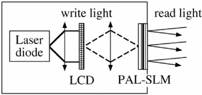
The structure of the device is described in figure 1. The PAL-SLM module consists of a liquid crystal layer, deposited on a dielectric mirror. Behind the mirror there is an amorphous silicon photoconductive layer. This structure is sandwiched between two transparent electrodes. The orientation of the liquid crystal molecules is determined by the electric field, which is controlled locally by changing the impedance of the photoconductive layer using a write beam, as shown in figure 1. The write beam is intensity modulated using a pixel liquid crystal device (LCD). Each pixel is controlled individually using a VGA signal from a computer, and the total active area is mm2. We note that since the readout light is completely separated from the LCD, diffraction effects due to the pixellized structure almost vanish, and the optical quality can be very high.
We measured the optical properties of the PAL-SLM using a Zygo phase-shift interferometer operating at 633 nm. When the SLM is switched off the reflectivity is greater than , and the wavefront distortion is 0.6 peak to peak over the whole surface and better than 0.1 over an active area of side 5 mm. We measured that the phase can be modulated between and 2.1 . For a given optical path length the phase shift is inversely proportional to the wavelength, so at our operating wavelength of 810 nm the maximum phase shift is reduced to 1.65 .
3 Hologram generation
The holograms are calculated using an iterative FFT algorithm, which exploits a numerical method to calculate the optimal phase modulation of the incident laser beam in order to obtain a desired intensity profile at the imaging plane [18, 19]. This algorithm works in the case of phase-only holograms. We will consider only regular arrays of optical traps, but the algorithm may be extended to more complicated structures with no lattice symmetries.
The basic idea is to find the relation between the intensity profile at the focal plane of the focusing objective that we want to obtain and the necessary phase modulation at the input plane. The wavefront at the focal plane can be written as :
| (1) |
and is the intensity profile that we want to obtain. The wavefront at the entrance pupil of the focusing objective is
| (2) |
where is the phase profile imposed by the hologram, that is the pattern we want to calculate. The input wavefront can be written as the inverse Fourier transform of the wavefront at the focusing plane:
| (3) |
We start by designing the array of traps we want to obtain in the focal plane as an array of Dirac delta functions, and we obtain by convoluting the array with the Airy pattern linked to the entrance pupil of the optical system. The algorithm is initialized by a guess of a phase distribution, which is used to calculate a pattern for the phase modulation of the input wave , as shown in the following diagram. The amplitude is chosen equal to one, as we do not change the amplitude of the input beam by modulating the phase only.
Following the diagram above, by Fourier transform we calculate the image on the focusing plane corresponding to this phase modulation at the input plane. The result will of course be different from the desired pattern. At this point the difference is reduced by multiplying the solution found by the desired pattern, . After normalizing this product ( being a constant to normalize the field amplitude), we take the inverse Fourier transform of the latter and we extract a phase pattern for the input beam that is closer to the required one. Then the cycle is repeated. This kind of algorithm converges within 3-4 iterations [18, 19].
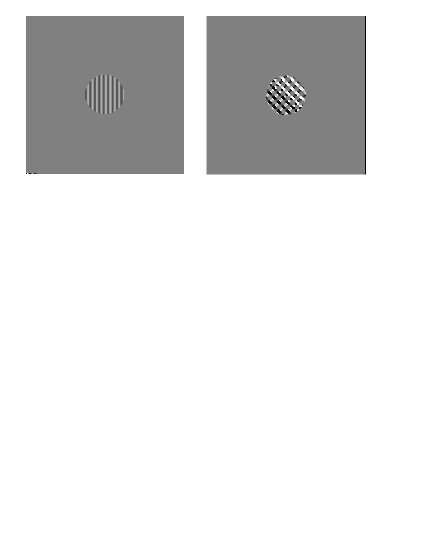
As examples of calculated holograms, figure 2 (left) shows the phase profile of the input wave used in order to obtain at the focusing plane of the objective an array of 3 dipole traps in a row separated by m. Figure 2 (right) shows the hologram calculated for obtaining an array of 5 dipole traps. These holograms were used to generate the trap arrays which will be presented in the following sections, see figure 6. These patterns are transmitted to the SLM by a standard VGA card. The different gray levels correspond to different phase shifts, with black and white giving a phase shift to . The phase modulation is calculated taking into account the size of the beam illuminating the PAL-SLM, so the modulated area in figure 2 corresponds to the size of the beam at the SLM position. Therefore only a fraction of the total area of the PAL-SLM is active for phase modulation.
Once the hologram is calculated, it can be modified by changing several parameters : the modulation area of the SLM can be reduced, increased or translated in order to optimize the matching with the beam’s size and position, and the modulation amplitude can be varied for optimal diffraction efficiency.
4 The dipole trap experiment
Our apparatus, described in [11, 13, 12], consists of a strongly focused dipole trap loaded from a magneto-optical trap (MOT) for Rubidium atoms. The MOT is loaded from an atomic beam, slowed down by chirped cooling. The dipole trap beam is focused by an objective placed inside the vacuum chamber (figure 3), with a numerical aperture of 0.7. This gives a measured beam waist of m, close to the diffraction limit [12]. The effective focal length is mm. This focused beam provides a tightly confining trapping potential at the center of the intersection region of the MOT beams. With a relatively small laser power of mW very high intensities can be reached at the focusing position ( kW cm-2). The dipole trap is operated in the far-detuned regime, the laser wavelength being nm, to be compared to the Rubidium atomic transitions at nm and at nm.
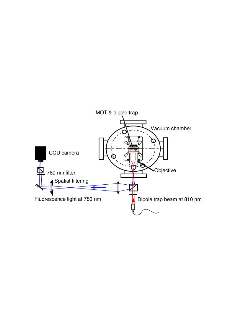
The trapped atoms are detected by using the fluorescence induced by the MOT beams at nm. The fluorescence is collected by the same objective which focuses the dipole beam and the detection system gives a magnified image of the trap on a charge-coupled device (CCD) camera, as shown in figure 3. A size of m on the focusing plane of the objective is imaged on 1 pixel of the CCD camera. The integration time is ms.
The dipole trap can be operated in several loading regimes [11, 13]. The loading rate of the dipole trap is proportional to the density of the MOT, which can be varied over several orders of magnitude by changing the intensity of the magnetic field gradient and the intensity of the slowing beams. When the MOT density is small (weak-loading regime) the lifetime of the atoms in the dipole trap is mainly determined by one-body decay due to collisions with the background gas. If the loading rate is increased, due to the very small trapping volume, there is a range of loading rates for which two-body collisions become the dominant term, allowing only one atom at a time to be stored in the trap. If a second atom enters the trap, a collision occurs and both atoms are ejected, as shown in ref. [11]. This “collisional blockade” mechanism operates only for very small trapping beam waists, typically less than m [11]. When the MOT density is high the loading rate is so high that the average number of atoms in the trap can reach typically (strong loading regime).
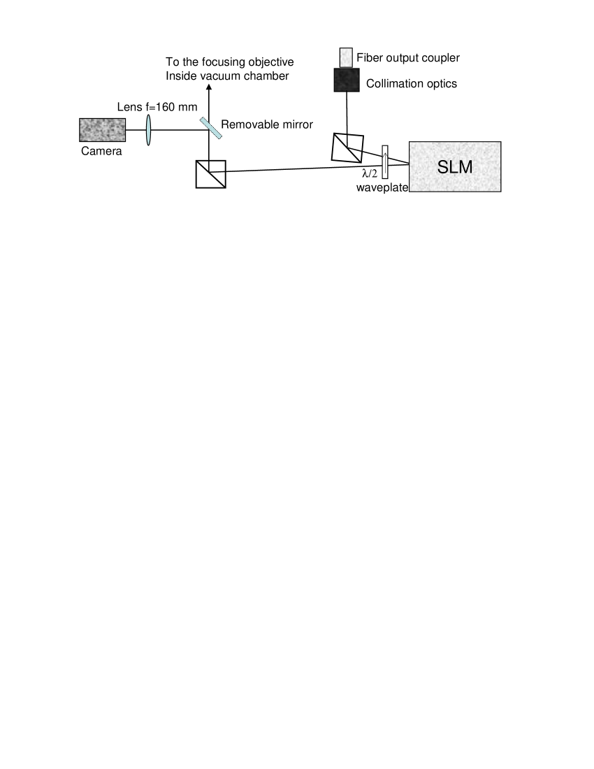
The dipole trap beam is produced by a nm laser diode and brought to the experiment using an optical fiber, and the PAL-SLM module is placed in the path of the dipole beam, as shown in figure 4. The beam waist at the SLM position was measured to be mm, so that an area of mm2 of the SLM was illuminated. The power of the incident beam was varied depending on the number of traps and trap depth that we wanted to obtain. The SLM can withstand laser intensities of up to mW/cm2. In order to maximize the diffraction efficiency the incident beam must be linearly polarized along the 0 voltage direction of the molecules, which was ensured by placing a plate in front of the SLM.
5 Experimental results
In this section we show how arrays of traps with different geometries were created, by sending holograms to the SLM. For simple geometries of the trap array, we can completely extinguish the trap corresponding to the zeroth-order diffraction spot. We also prove that we can control the position of the traps with micrometer precision. Finally, we used a simple array geometry to confine single atoms at distinct trapping sites.
5.1 Tests with different geometries
Different holograms were calculated with the iterative FFT algorithm described in section 3. Each calculated hologram was optimized using an auxiliary lens, with a focal length of 160 mm, focusing the generated pattern on a standard CCD camera (see figure 4).
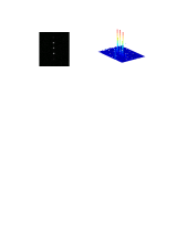
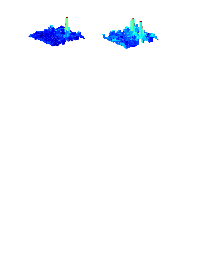
As an example, the intensity profile of a 3-spot array is shown in figure 5. The three dimensional plot shows that the three spots have equal intensity. By adjusting the hologram, as explained in section 3, we can optimize the symmetry of the intensity profile, remove higher order diffraction spots, and control the zeroth-order.
The light was then sent on the atomic sample. We monitored the resulting fluorescence pattern and fine tuned the hologram in order to obtain the desired trapping configuration.
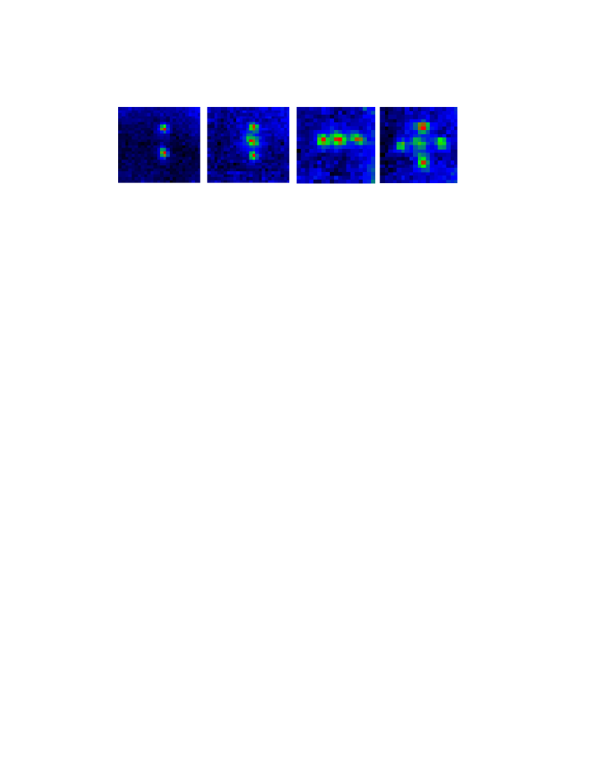
The resulting fluorescence pattern from the trapped atoms for four different holograms is shown on figure 6. For these pictures we worked in the strong loading regime, and so each trap contains a few tens of atoms. Figure 6 (left) shows two traps generated symmetrically with respect to the zeroth-order, which has been suppressed completely. The second and third panels of figure 6 show arrays of three dipole traps obtained using the phase modulation pattern shown in figure 2 (left), rotated by either or in the SLM plane. Finally five traps were generated, using the hologram of figure 2 (right). The limited total laser power available did not allow us to test structures with larger number of traps, but we have successfully calculated holograms with symmetric spots, and hexagonal geometries.
We limited our tests to two-dimensional geometries, but three-dimensional configurations are also possible. The focusing plane could be changed by adding a lens to the beam path, so that its convergence can be changed. The effect of the lens can be easily reproduced by adding a quadratic phase modulation to the existing hologram. Therefore, by dynamically changing the computer signal sent to the SLM it is possible also to create a three-dimensional trap array, and to change the geometry and the positions of the traps [20, 21].
5.2 Controlling the zeroth order.
One of the main issues in using an essentially diffractive optical element is the zeroth-order diffraction spot. Although very high diffraction efficiency can be achieved, the residual zeroth-order diffraction spot cannot always be easily controlled for the design of the pattern. Here we will show that it is possible to either completely extinguish the trapping site associated to the zeroth order beam, or to exploit it to create arrays of equally intense traps.
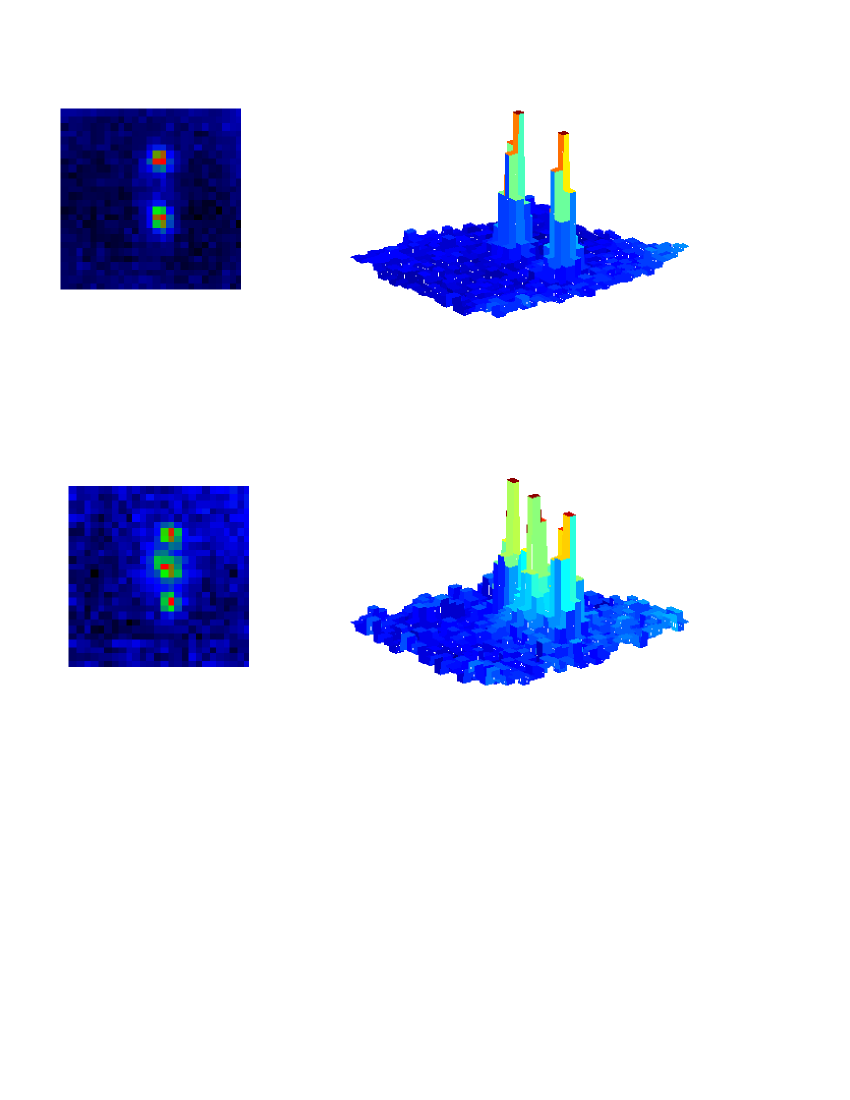
In figure 7 the images taken for two and three traps are shown. We note that the two traps are generated symmetrically with respect to the zeroth order diffraction spot, and that the middle trap in the three traps array is generated with the zeroth-order. We are therefore capable to take into account the zeroth order in our calculations and control finely its intensity, so that we can generate arrays of traps where the zeroth order is suppressed. Actually, we exploit the experimental observation that there is a trapping depth threshold, below which the atoms cannot be captured. Therefore, the central peak actually disappears as soon as the intensity is below the threshold required to capture atoms, even if the trap light intensity has not completely vanished. This method provides good enough control that we are not limited by the zeroth-order diffraction spot for simple geometries.
5.3 Varying the relative distance
It is also possible to fully control the relative position of the trapping sites, either between experiments or dynamically, just by changing the hologram supplied to the device as a VGA signal. The lattice constant can therefore be changed as well as its geometry.
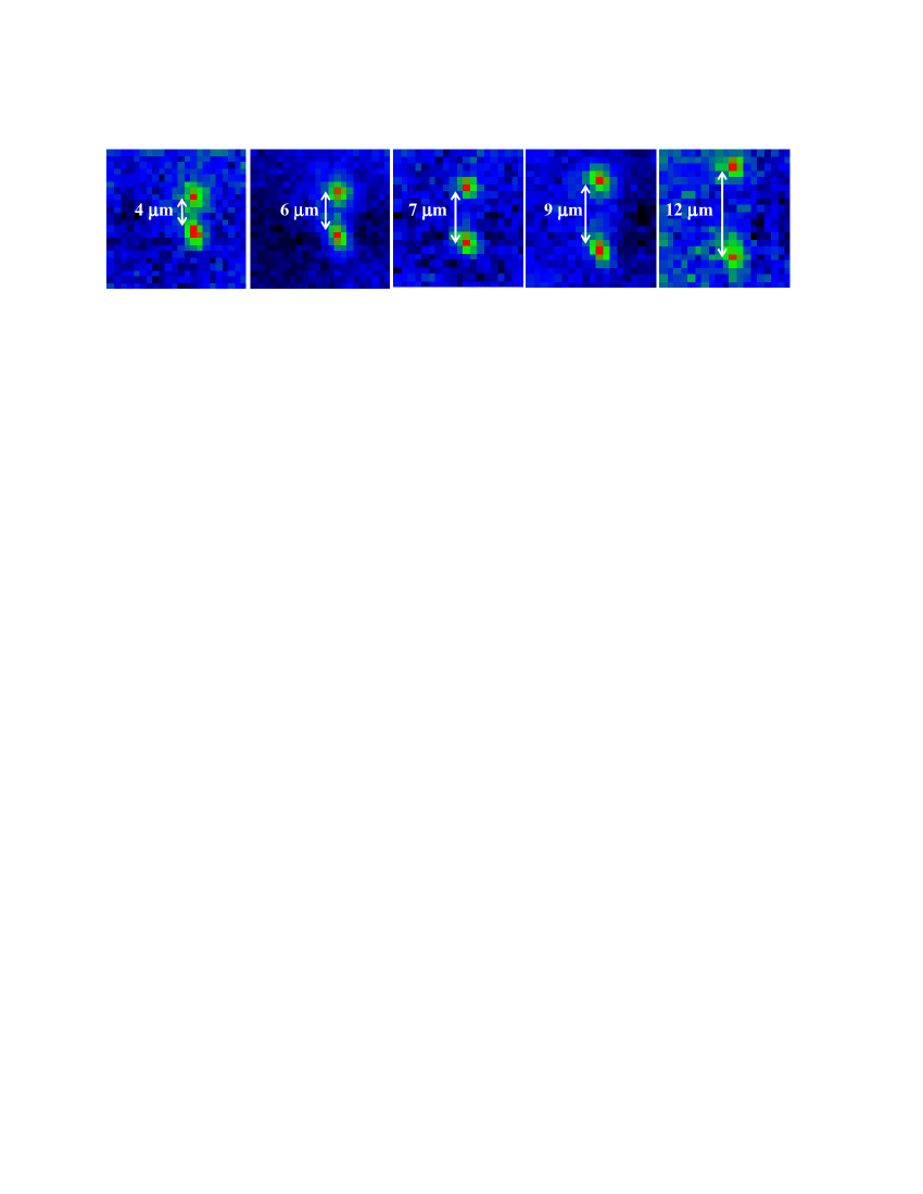
This is illustrated on figure 8, where we show how to control the relative distance of two traps with m accuracy. The trap separation in one array at the imaging plane depends on the periodicity of the phase modulation:
| (4) |
where is the laser wavelength, is the focal distance of the objective, and is the phase modulation period. So in the case of simple geometries, where there is a lattice structure, the separation between the traps can be changed by modifying the period of the lattice. Our measurements were limited by the magnification of the imaging system, for which one micron on the focusing plane is imaged on one pixel.
From equation 4, the minimum change in the trap separation is associated to the minimum change in the phase modulation period, which is given by the size of 1 pixel of the SLM ( m). For our present (non-optimized) set-up, and for the case of m separation of figure 8, this gives a limit of precision of the trap position of 300 nm.
In more complicated geometries with many traps, the moving of only one of the traps with respect to the others can be achieved in real-time, by sending sequences of pre-calculated holograms to the SLM. Dynamical control of the trap position is dependent on the response time of the SLM itself, and on the update rate of the driving VGA signal. Currently the refresh rate of available systems using nematic crystals (including the Hamamatsu SLM used here) is limited to a few tens of Herz. Higher speed (in the kHz range) can be achieved in principle with commercial ferroelectric liquid crystals [22], which have however a lower diffraction efficiency. Therefore the current performance for the moving speed of the traps does not quite allow fast enough control for gate operations.
This limitation can be overcome using schemes which rely on the combination of an array of (slowly) reconfigurable traps, and of a fast “moving head”, which can be realized with a laser beam driven by 2D acousto-optic modulators (beam scanners). Such a scheme would be a neutral atom analog of the proposal of ref. [23] for ion traps.
5.4 Single atom trapping
Finally, we tested the hologram-generated three-trap configuration for single atom trapping. By decreasing the density of the atomic cloud it is possible to enter the regime of loading in which either one or zero atom is trapped per each site. In figure 9 (left) a single atom is captured in one trap and its fluorescence is detected with a 200 ms integration time. On the right side, two atoms are simultaneously loaded in two distinct traps. The traps are generated with a laser power of mW for each one, which is just above the threshold laser power to capture one atom. Working close to the threshold trap intensity minimizes the light shift induced by the trapping beam, and therefore maximizes the MOT-induced fluorescence signal for a single atom.
Some considerations can be made about the quality of the traps generated with the hologram. For instance, by comparing the threshold laser power for traps generated by diffracted beams with the threshold laser power for trapping with the non diffracted beam, and assuming that the trapping threshold only depends on the depth of the trap, we can give a better estimate of the maximum beam waist enlargement. The trap depth is proportional to the laser power and inversely proportional to the square of the beam waist, so if a change in laser power is necessary in order to reach the trapping threshold this can be easily related to a change in the beam size. From these considerations we estimate an upper limit for the waist enlargement of per cent with respect to the non diffracted beam, which means an upper limit for the waist of the diffracted beams of just over 1 m.
In the collisional blockade regime, two-body collisions lock the average number of atoms to [11]. This means that in these operating conditions the theoretical probability of detecting one atom in one of the traps is . The probability of detecting three atoms being simultaneously stored in three distinct traps therefore drops down to . Unbalance in the trap depth would further reduce this probability. Referring to figure 9(b),we found that the trap that is not lit showed a probability of storing a single atom, which is probably due to a shallower trap depth, linked to an asymmetry in the generated intensity pattern.
6 Conclusion
We have demonstrated the possibility of creating multi-trap arrays for single atoms using a nematic liquid crystal spatial light modulator. The advantage of using such a device is that it is fully programmable and computer controllable : multiple traps can be generated in different geometries and the position of the traps can be designed from the VGA signal sent to the module. Arrays of traps, each capable of storing a single atom, can be dynamically modified, allowing the real-time motion of one or more traps with respect to the array.
This opens up possibilities for testing the proposed schemes for atom-atom entanglement. For instance, qubit encoding on the motional state of an atom in a dipole trap was proposed in [9]. In another scheme [8], the qubit is encoded in the motional state of one atom, which can be trapped in either of two traps with an adjustable separation. Both proposals [9, 8] are studied for Rb micro-dipole traps, for which single-atom storage has been obtained with our setup. Single qubit operations are achieved by moving the traps adiabatically and bringing them closer so that tunneling between the two wells is allowed, and two-qubit operations are realized via collisions between two atoms stored in distinct traps.
Alternatively, qubits can be encoded in single atoms trapped at different locations by using the hyperfine structure of the ground state, the initialization and single-qubit operations being achieved with Raman pulses. Two-qubit operations then require either controlled cold collisions as implemented recently [10], or long-range coupling as proposed in [2, 3].
Aknowledgements
The authors acknowledge the contribution of Arnaud Pouderous and Michael Scholten to early stages of the experiment. We are indebted to Sébastien Bouilhol from Hamamatsu for the loan of the PAL-SLM. This work is supported by the IST / FET / QIPC project “QGATES”, and by the European Research Training Network “QUEST”.