Current address: ]Department of Physics, Ben Gurion University, Beer-Sheva 84105, Israel
An atom fiber for guiding cold neutral atoms
Abstract
We present an omnidirectional matter wave guide on an atom chip. The rotational symmetry of the guide is maintained by a combination of two current carrying wires and a bias field pointing perpendicular to the chip surface. We demonstrate guiding of thermal atoms around more than two complete turns along a spiral shaped 25mm long curved path (curve radii down to 200m) at various atom–surface distances (35-450m). An extension of the scheme for the guiding of Bose-Einstein condensates is outlined.
pacs:
The fast development of new tools for the precise control and manipulation of neutral atoms makes a great variety of novel experiments feasible. In particular, the adaption of microfabrication techniques in atom optics laboratories has lead to the implementation of atom chips Folman et al. (2002); Reichel (2002). The patterned surfaces of these devices allow trapping and guiding of atoms with the high accuracy given by the fabrication process. Possible applications of atom chips are abundant, fundamental studies of degenerate quantum gases in low dimensional potentials and mesoscopic physics in small atomic ensembles being just two prominent examples. In the quest for implementations of quantum information processing (QIP) with neutral atoms, atom chips are especially promising candidates.
The versatility of atom chips has been shown in a number of experiments. After the demonstration of simple magnetic trapping and guiding potentials Reichel et al. (1999); Folman et al. (2000), the production of Bose-Einstein condensates (BEC)Ott et al. (2001); Hänsel et al. (2001); Leanhardt et al. (2002); Schneider et al. (2003) and the integration of electrostatic fields Krüger et al. (2003) on the chips have been important milestones on the way to a fully functional toolbox for the control of atomic matter waves. Issues currently under investigation include the integration of light elements for enhanced detection efficiency of (single) atoms Horak et al. (2003) and the coherence properties of atoms in the chip potentials Henkel et al. (2003).
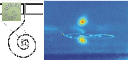
Here, we report on the implementation and experimental test of a key element for the controlled manipulation of matter waves on the atom chip: an omnidirectional ‘atom fiber’, i.e. an atomic wave guide based on a potential that is independent of the guiding direction (Fig. 1). The use of such an element is inevitable when atoms are to be transported to and stored in individual trapping sites on the two dimensional surface of the chip. This will be of particular significance for implementations of quantum registers for QIP based on a 2-dimensional array of microtraps. Furthermore, the directional symmetry of this type of guide is crucial for guided matter wave interferometers that rely on spatially symmetric beam splitters, i.e (wide angle) Mach-Zehnder and Sagnac interferometers.
The simplest form of a magnetic wire guide is the side guide in which atoms in weak field seeking states () are trapped in a potential tube along a line parallel to a straight current carrying wire (Fig. 2a). To achieve this configuration, the field of the wire is superimposed with a homogenous external bias field. Atoms can only move along the third unconfined direction as long as the bias field points in the direction perpendicular to the guiding direction. This implies that the side guide is only a single-directional guide 111Small angular deviations from the straight guiding path can be tolerated for thermal atoms as long as the potential barriers along the guide are small compared to the atom cloud temperature.. True multi-directional guiding is only possible for guides based on at least two current carrying wires. One possible two-wire guide is based on two parallel wires carrying co-propagating currents. In this case, no additional bias field is needed and the guide can be shaped simply by bending the wires. Wire guides with two co-propagating currents have been realized and it has been shown that atoms can be deflected by small angles Müller et al. (1999) and even be stored in a complete loop where a cloud has been observed to move around a number of full turns Sauer et al. (2001). A drawback, however, lies in the fact that the rotational symmetry of the potential can only be maintained when no external bias field is added. This implies that the potential minimum will always be located in the center between the two wires which limits the flexibility severely.
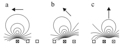
An improved type of two-wire guide is based on parallel counter-propagating currents (Fig. 2c). Here, the field of the wires can be compensated by a field pointing perpendicular to the wire plane which avoids the usual symmetry breaking associated with the addition of an external homogenous field. Together with the currents, the strength of the bias field determines the height of the guide above the wire plane and the potential parameters Thywissen et al. (1999). In a first experiment, a free falling atomic cloud has been observed to be guided by a straight two-wire guide with counter-propagating currents Dekker et al. (2000).
In our experiment, we set out to demonstrate deterministic loading and actual guiding of atoms confined in a bent two-wire guide with counter-propagating currents. For this purpose, we designed a spiral shaped two-wire guide (Fig. 1). The two wires (width height m2, center to center spacing m) are connected at the inner end of the spiral. This automatically leads to a counter-propagating current flow. The spiral shape was chosen in order to demonstrate the full flexibility of the guide by incorporating more than two full rotations with curve radii ranging from 200m to 3mm along the 25mm long guiding path. The U-shaped wires (cross section m2) on either side of the straight beginning of the guide are used to form three dimensional traps Folman et al. (2002).
The starting point of our atom chip experiments is a reflection magnetooptical trap (MOT) Reichel et al. (1999) that contains a cloud of typically cold 7Li atoms located a few millimeters above the chip surface. The magnetic quadrupole field for the MOT is initially provided by external coils and after the loading replaced by the field of a U-shaped wire (mm) mounted directly underneath the chip. This allows to bring the atoms closer to the surface and to transfer them to a purely magnetic trap formed by the same magnetic field. In the next step, the cloud is loaded to the magnetic potentials produced by wires on the chip. The details of this procedure are given in Folman et al. (2000); Cassettari et al. (2000).
In order to transfer the atoms from a U-wire trap, i.e. a trap based on a single wire and a horizontal bias field, to the spiral shaped two-wire guide, we ramp down the current of the single wire while ramping up the counter-propagating currents in the two parallel wires of the guide. During this first step, the bias field is only partially rotated so that the bending of the wires still provides an endcap of the potential, thus confining the atoms in three dimensions. As depicted schematically in Fig. 2b, this intermediate configuration is reminiscent of the simple side guide (Fig. 2a) with only a slight perturbation by the current in the extra wire. In the final step, the rotation of the bias field is completed (Fig. 2c), and the atoms can expand freely along the spiral shaped path of the guide.
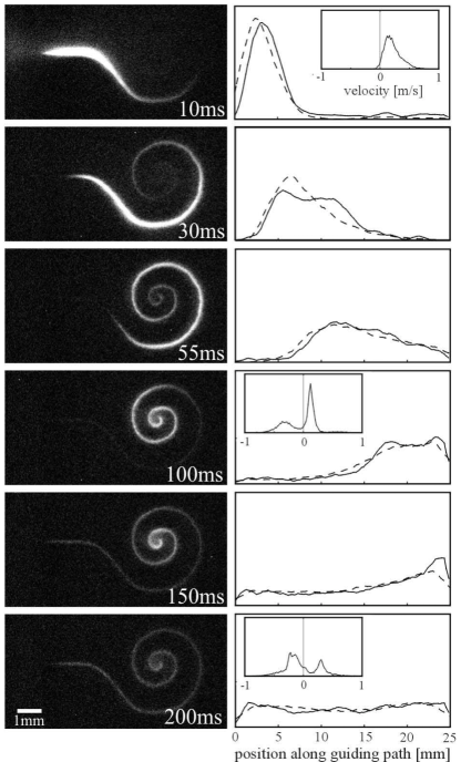
Fig. 3 shows a time sequence of the fluorescence signal of atoms in the guide 222The images are taken by exposing the atoms to a flash (100s) of near resonant laser light. In order to avoid any disturbing reflections, the light enters the chamber from two directions parallel to the chip surface.. Guiding of atoms was possible over a wide range of parameters. By varying the bias field strength from 1G to 50G at a constant current of 1A through both (connected) wires, the height of the potential tube above the surface was scanned from 450m to 35m and corresponding gradients of 40G/cm to 8kG/cm for atoms in the state. The images and density profiles in Fig. 3 show that the atom cloud not only expands according to its temperature 333The clouds exhibit an anisotropic temperature profile (450K in the transverse, 50K in the longitudinal direction) due to a transverse compression during the loading without rethermalization. but also moves as a whole along the guide. This center of mass motion is induced by a longitudinal field gradient produced by the current in the two leads from the beginning of the spiral wires to the connecting pads on the edge of the chip 444By running a parallel current through another wire on the chip, we could even enhance this ‘pushing’ effect..
For a quantitative understanding of the density profiles, we performed Monte-Carlo (MC) simulations of classical trajectories of particles in the guide. The results are depicted in Fig. 3 and show good agreement with the experiment. In particular, the reflections that occur when atoms reach the inner end of the guide, are reproduced well. The effect of the reflection becomes most apparent in the plots of the velocity distributions extracted from the MC calculations (inserts). The velocity classes for forward and backward motion in the guide are clearly separated.
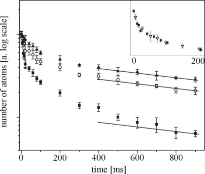
For a characterization of the guides, lifetimes of confined atom clouds are of great significance. In our single vacuum chamber apparatus, the rest gas pressure is typically of the order of mbar, corresponding to background gas collision limited lifetimes of s as was confirmed in a conventional single Z-wire trap Folman et al. (2002).
Direct lifetime measurements in the guide were only carried out for guiding times of up to ms 555Ohmic heating in the long guiding wires did not allow longer guiding times without risking damage to the wires.. Indirect lifetime measurements were performed in three dimensionally confining potentials based on counter-propagating currents through two parallel wires. For this purpose we used the two U-shaped wires (Fig. 1) where the confinement in the longitudinal direction is provided by the wire leads. In these traps, the lifetime measured in the conventional Z-trap could be reproduced for the long trapping time regime (300ms). For shorter times, the shape of the potential leads to a faster additional loss of the hottest atoms on a timescale of ms. This behavior was again confirmed by MC-calculations and will not pose a problem for colder atom samples. The measured results for different potential depths are depicted in Fig. 4. The comparison of the data obtained for the guide and for the three-dimensional trap (insert) shows complete agreement on the short timescale indicating the validity of the indirect measurements also for longer times.
In future applications of vertical bias field guides, it will be crucial to be able to guide much colder atoms (ideally BEC) than the ones used in our demonstration and characterization. In this case, a loss mechanism that does not play a role in the experiments presented here will be dominating: Majorana spin flip transitions will remove atoms from the guide in the vicinity of the quadrupole minimum of the potential where the field vanishes. The usual remedy employed in single-directional guides is the addition of a small field component pointing in the guiding direction (Ioffe-Pritchard (IP) field). For a multi-directional guide this would mean that a locally varying field would have to be used or, alternatively, the IP field could be rotated as a (small) cloud moves along the guide.
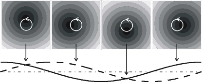
Here, we suggest a solution that we believe to be more flexible and easier to implement experimentally. Sinusoidally modulating the currents according to in the two (now separated) guiding wires with a relative phase difference of leads to a (nearly) circular motion of the quadrupole minimum of the guide (Fig. 5). As long as the modulation frequency is slow with respect to the Larmor frequency but fast with respect to the atomic oscillation frequency , the atoms can be described as moving in a time averaged (orbiting) potential (TOP). Such TOP are routinely used for the production of Bose-Einstein condensates Petrich et al. (1995). If the height of the guide over the wire plane is equal to the half distance between the wires, the parameters of the averaged potential are and with the vacuum permeability , the Bohr magneton , the Landé factor , and the atomic mass . The depth of the potential is given by the radius of the circle of vanishing field (‘circle of death’) . The potential tuning range is large, a TOP two wire (m) atom fiber for a BEC with kHz, kHz and m could, for example, be obtained with mA, mA, and G (87Rb atoms in the in the state).
To conclude, we have demonstrated the controlled loading and guiding of atoms in a truly omnidirectional guide that exhibits complete rotational symmetry. The flexibility of the guide was proven by operating it over a wide parameter range. Monte-Carlo simulations reproduce the measured time dependent atomic density profiles well. We have discussed a scheme involving time dependent currents to modify the guide in order to lift the current restriction to thermal atoms. Future applications range from the loading of two-dimensional trap arrays to the realization of circular of wide angle matter wave interferometers Andersson et al. (2002).
Acknowledgements.
This work was supported by the European Union, contract numbers IST-2001-38863 (ACQP), HPRI-CT-1999-00114 (LSF) and HPRN-CT 2002-00304 (FASTNet) and the Deutsche Forschungsgemeinschaft, Schwerpunktprogramm ‘Quanteninformationsverarbeitung’.References
- Folman et al. (2002) R. Folman, P. Krüger, J. Schmiedmayer, J. Denschlag, and C. Henkel, Adv. At. Mol. Opt. Phys. 48, 263 (2002).
- Reichel (2002) J. Reichel, Appl. Phys. B 74, 469 (2002).
- Reichel et al. (1999) J. Reichel, W. Hänsel, and T. W. Hänsch, Phys. Rev. Lett. 83, 3398 (1999).
- Folman et al. (2000) R. Folman, P. Krüger, D. Cassettari, B. Hessmo, T. Maier, and J. Schmiedmayer, Phys. Rev. Lett. 84, 4749 (2000).
- Ott et al. (2001) H. Ott et al., Phys. Rev. Lett. 87, 230401 (2001).
- Hänsel et al. (2001) W. Hänsel et al., Nature 413, 498 (2001).
- Leanhardt et al. (2002) A. E. Leanhardt et al., Phys. Rev. Lett. 89, 040401 (2002).
- Schneider et al. (2003) S. Schneider et al., Phys. Rev. A 67, 023612 (2003).
- Krüger et al. (2003) P. Krüger et al., (2003), quant-ph/0306111, accepted to Phys. Rev. Lett.
- Horak et al. (2003) P. Horak et al., Phys. Rev. A 67, 043806 (2003).
- Henkel et al. (2003) C. Henkel, P. Krüger, R. Folman, and J. Schmiedmayer, Appl. Phys. B 76, 173 (2003), and references therein.
- Müller et al. (1999) D. Müller et al., Phys. Rev. Lett. 83, 5194 (1999).
- Sauer et al. (2001) J. A. Sauer, M. D. Barret, and M. S. Chapman, Phys. Rev. Lett. 87, 270401 (2001).
- Thywissen et al. (1999) J. H. Thywissen et al., Eur. Phys. J. D 7, 361 (1999).
- Dekker et al. (2000) N. H. Dekker et al., Phys. Rev. Lett. 84, 1124 (2000).
- Cassettari et al. (2000) D. Cassettari et al., Phys. Rev. Lett. 85, 5483 (2000).
- Petrich et al. (1995) W. Petrich et al., Phys. Rev. Lett. 74, 3352 (1995).
- Andersson et al. (2002) E. Andersson et al., Phys. Rev. Lett. 88, 100401 (2002).