Optical-fiber based measurement of an ultra-small volume high- photonic crystal microcavity
Abstract
A two-dimensional photonic crystal semiconductor microcavity with a quality factor and a modal volume cubic wavelengths is demonstrated. A micron-scale optical fiber taper is used as a means to probe both the spectral and spatial properties of the cavity modes, allowing not only measurement of modal loss, but also the ability to ascertain the in-plane localization of the cavity modes. This simultaneous demonstration of high- and ultra-small in an optical microcavity is of potential interest in quantum optics, nonlinear optics, and optoelectronics. In particular, the measured and values could enable strong coupling to both atomic and quantum dot systems in cavity quantum electrodynamics.
pacs:
42.60.Da, 42.50.Pq, 42.70.QsThe use of an optical microcavity to alter the interaction of light with matter has been instrumental within a wide range of fields, including cavity quantum electrodynamics (cQED) Kimble (1998), nonlinear optics Chang and Campillo (1996), and molecular sensing Norris et al. (1997). This interaction depends strongly upon the cavity photon lifetime, measured by the quality factor , and the electromagnetic energy density within the cavity, quantified by the effective modal volume 111 is defined as the electric field energy within the cavity normalized to the peak electric field energy density Foresi et al. (1997). Planar photonic crystal (PC) microcavities have attracted significant attention Painter et al. (1999); Foresi et al. (1997); Ryu et al. (2002); Srinivasan and Painter (2002) in this regard due to their ability to trap light within volumes approaching the theoretical limit Painter et al. (1999), the potential for on-chip integration with waveguides Noda et al. (2000); Smith et al. (2001); Barclay et al. (2003), and lithographic control of many salient properties of the cavity modes Painter et al. (2001). A major limitation, however, has been the relatively low experimentally-realized values, limited to Yoshie et al. (2001) until recent demonstrations of in an add-drop filter Akahane et al. (2003) and Srinivasan et al. (2003) in a sub-threshold laser cavity. In this Letter, we present optical fiber taper measurements of a PC microcavity supporting a mode with and in-plane localization consistent with cubic wavelengths (). This simultaneous realization of a high- and ultra-small- PC microcavity is of importance to a number of applications in the aforementioned disciplines, while the fiber taper probe is of potential value to future studies of wavelength-scale resonators.
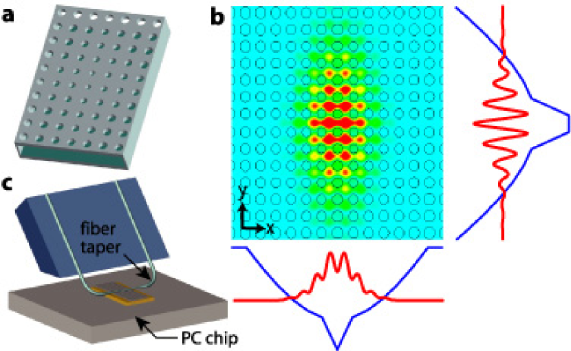
The PC cavity geometry employed is shown in Figure 1a,b, and was designed using group theoretical, Fourier space, and finite-difference time-domain (FDTD) analyses as described in detail elsewhere Srinivasan and Painter (2002). The cavity consists of a localized defect in a square lattice of air holes that are etched into an optically thin membrane of refractive index . This geometry provides in-plane modal localization via distributed Bragg reflection due to the lattice and vertical confinement by total internal reflection at the membrane-air interface. The resulting TE-like (electric field in the plane of the slab) defect mode (so labelled due to its symmetry and ground-state frequency in the cavity) shown in Fig. 1b is predicted to have and , where is the wavelength of the resonant cavity mode. The important aspects of the cavity design are: (1) the dominant electric field component, , is odd about the -axis, thereby reducing vertical radiation loss from the patterned slab, (2) a grade in the hole radius is used to both further confine the mode in-plane and reduce in-plane radiative losses, and (3) the design is relatively insensitive to perturbations to the cavity, as verified through simulations where the steepness of the grade and the average hole radius () have been varied significantly without degrading the below .

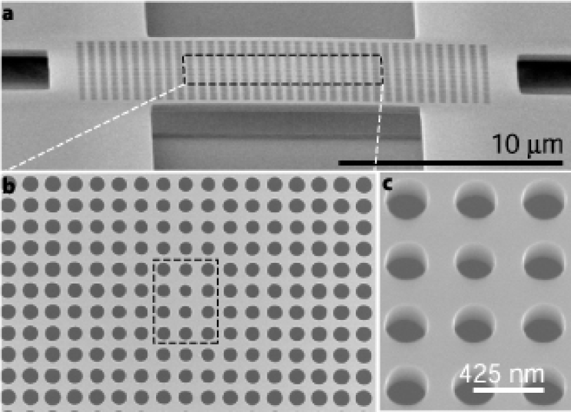
In this work, PC membrane microcavities are formed from a silicon-on-insulator wafer consisting of a nm thick silicon (Si) layer on top of a 2 m silicon dioxide layer (although Si was chosen here, similar high refractive index PC microcavities have been fabricated in a wide range of semiconductors, including AlGaAs-based Yoshie et al. (2001) and InP-based Srinivasan et al. (2003) systems). Cavities are fabricated using electron beam lithography, a plasma etch through the Si layer, and a hydrofluoric acid wet etch to remove the underlying oxide layer. Fully processed chips consist of a linear array of cavities, with lattice constant () varying between - nm and with - different lattice filling fractions (or equivalently, ) for a given . Scanning electron microscope (SEM) images of a fabricated device are shown in Fig. 2.

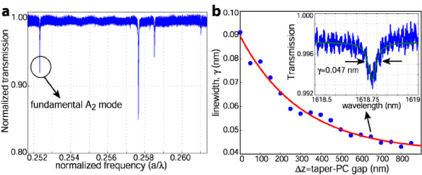
To study the resonant modes of the PC microcavities an optical fiber-based probe is used. Optical fiber tapers Knight et al. (1997); Birks and Li (1992) are fabricated by heating and stretching a standard single mode fiber to a diameter of - m, providing an air-guided fundamental mode with an evanescent tail extending into the surrounding air. The taper is mounted so that it can be laterally and vertically positioned over the cavities (Fig. 1c), and is connected to a scanning tunable laser with 1 pm resolution and a - nm wavelength scan range. When the taper is brought close ( nm) to the surface of a given cavity, a number of resonance features in the taper transmission appear (Fig. 3a). These features disappear if the taper is positioned to the side of the cavity or if the polarization of the input light is adjusted to be TM-polarized relative to the PC slab. The resonance positions shift as a function of and in a manner consistent with that expected for modes supported by the photonic lattice Joannopoulos et al. (1995). Noting that the defect mode of Fig. 1 is the lowest frequency mode lying within the (partial) photonic band-gap of the lattice, an experimental spectral identification of this mode is made for fixed as follows. Devices are tested as a function of decreasing , so that initially, when the devices have large-sized holes, all of the resonant modes formed from the appropriate photonic band-edge lie above the frequency scan range of the input laser. We then test in succession cavities with decreasing until a resonance is observed. This resonance is the lowest frequency mode lying within the in-plane (partial) bandgap of the photonic crystal, and thus corresponds to the cavity mode of interest, the fundamental mode.
A wavelength scan of the taper transmission showing the resonance of the mode for a device with =425 nm is given in the inset of Fig. 3b. In this measurement the taper is positioned parallel to the -axis at a height of nm above the center of the PC microcavity. Fitting this transmission data to a Lorentzian, a linewidth nm is measured for the cavity resonance. This linewidth is a maximum estimate for the cold-cavity linewidth due to cavity loading effects of the taper. Loading by the taper results in out-coupling to the forward propagating fundamental taper mode which, upon interference with the power directly transmitted past the cavity, results in the observed resonant feature in the taper transmission. Other parasitic taper loading effects include coupling to radiation modes, higher-order taper modes, and the backward propagating fundamental taper mode. To estimate the taper loading effects on the cavity mode, we examine as a function of . The resulting data (Fig. 3b) shows that as increases, the loading effects are reduced, until a regime is reached where the taper does not significantly effect the cavity mode and the measured linewidth asymptotically approaches the cold-cavity linewidth. Assuming that the loading is monoexponentially related to , we fit the measured linewidth to the function , where , , and are all fitting parameters. The resulting fit value of is nm, essentially identical to the directly measured linewidth when nm, and corresponds to a cold-cavity . To compare this result directly with numerical calculations, we repeat our previous FDTD calculations Srinivasan and Painter (2002) but include an offset in of to account for the increased size of the fabricated holes (as measured by SEM) relative to the design of Fig. 1. Doing so yields a predicted and , fairly close to the measured values, and a , smaller than the original design due to the better in-plane confinement provided by the larger hole radii. As a final comment on , we note that a number of devices encompassing a range of values for and the grade in have been tested, and values have been consistently measured, in accordance with simulation results. As described earlier, this robustness to deviations from the ideal structure is perhaps the most important aspect of the cavity design.

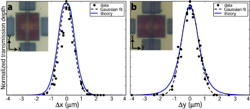
By measuring (for fixed ) the strength of the coupling to the PC cavity modes as a function of lateral taper displacement, the in-plane localization of the cavity modes can be ascertained Knight et al. (1995), 222Here the same optical fiber taper near-field probe is used to both excite the PCWG modes and to map their spatial profile. Other works employing evanescent coupling from eroded monomode fibers to excite silica microsphere whispering-gallery modes have used a secondary fiber tip to collect and map the mode profiles Knight et al. (1995).. The strength of coupling is reflected in the depth of the resonant dip in the taper transmission 333The maximum transmission depth achieved for the mode of interest was , though coupling to other modes reached depths as large as . Coupling in all cases was limited to the under-coupled regime Cai et al. (2000).. For the taper aligned along the long () and short () axes of the cavity the depth of the resonant transmission dip for the cavity mode versus taper misalignment is shown in Figs. 4a and 4b, respectively. These measurements show the mode to be well-localized to a micron-scale central region of the cavity, and confirm that the mode is both high- and small . They do not, however, reveal the highly oscillatory cavity near-field, but rather an envelope of the field, due to the relatively broad taper field profile. To better understand the results of Fig. 4, we consider a simple picture of the taper-PC cavity coupling Haus (1984), where the coupling coefficient is calculated from the analytically-determined taper field and the phase-matched Fourier components of the FDTD-generated cavity field. The calculated resonant transmission depth as a function of taper displacement is shown in Figs. 4a,b as solid lines and agrees closely with the measured data. Assuming that the cavity mode is localized to the slab in the -direction, the close correspondence between the measured and calculated in-plane localization indicates that for this high- mode. Similar measurements of the higher-frequency resonant modes of the PC microcavity (such as those in Fig. 3a) indicate that they are significantly more delocalized in-plane in comparison to the mode, as one might expect for higher-order modes of the cavity.

To illustrate the potential applications of such a small and high- microcavity, we consider two examples from quantum optics. The Purcell factor (), a measure of the microcavity-enhanced spontaneous emission rate of an embedded active material, is given under suitable (maximal) conditions as Gayral et al. (1999):
| (1) |
For the PC microcavity studied here (, ), the predicted is , an extremely large value for a semiconductor-based microcavity (previous work on semiconductor microdisks Gayral et al. (1999) have predicted ). Another application is in cQED, where strongly coupled atom-photon systems have been proposed as candidates to produce the quantum states required for quantum computing applications Mabuchi and Doherty (2002). For such applications, the regime of strong coupling Kimble (1998), where the atom-photon coupling coefficient () exceeds the cavity and atomic decay rates ( and , respectively), must be reached. Although strong coupling has been achieved in systems consisting of an alkali atom and an actively-stabilized Fabry-Perot cavity Kimble (1998), in future applications, where higher levels of integration are sought, chip-based cavities are of interest Mabuchi and Doherty (2002). Using the measured and estimated for the mode studied here, the relevant parameters for a commonly-used Cesium (Cs) atomic transition ( nm, MHz) Kimble (1998), and the formulas and , we calculate GHz 444As is defined relative to peak electric field energy density, rather than electric field strength, a factor must be included for dielectric cavities where the two values are not equal. for our cavity. and GHz, indicating that the coupled Cs-PC cavity system could achieve strong coupling. In addition, the calculated critical atom number () and saturation photon number () are and , a regime where a single atom would have a profound effect on the cavity field, and vice versa. A similar calculation for an InAs semiconductor quantum dot Becher et al. (2001) indicates that the current PC microcavity would also be capable of reaching strong coupling in such a solid-state system.
In conclusion, while silica fiber tapers have been successfully used to probe larger () silica-based resonators, such as microspheres Knight et al. (1997); Cai et al. (2000) and microtoroids Armani et al. (2003), the current work illustrates the use of tapers as a probe for ultra-small mode volume, high refractive index () cavities, where the micron-scale dimension of the taper is utilized to both source and out-couple light from the cavity. This technique allows for rapid characterization of relevant cavity mode parameters (, , and ), and although it does not necessarily provide efficient coupling to the cavity [28], as a suitably designed waveguide may Barclay et al. (2003), the use of an external fiber-based probe provides a greater level of versatility than other methods, such as embedding of active material within the cavity Yoshie et al. (2001); Srinivasan et al. (2003) or microfabrication of input-output waveguides to couple to the cavity Noda et al. (2000); Lin et al. (2001). In particular, resonant cavity elements in both passive and active devices can be tested, making it a valuable tool for future studies of wavelength-scale resonators. Here, we have used this technique to demonstrate a PC microcavity mode with and in-plane localization consistent with .
The authors thank B. Lev and H. Mabuchi for useful discussions pertaining to cQED. K.S. thanks the Hertz Foundation and M.B. thanks the Moore Foundation, NPSC, and HRL Laboratories for their graduate fellowship support.
References
- Kimble (1998) H. J. Kimble, Physica Scripta T76, 127 (1998).
- Chang and Campillo (1996) R. K. Chang and A. J. Campillo, eds., Optical Processes in Microcavities (World Scientific, Singapore, 1996).
- Norris et al. (1997) D. J. Norris, M. Kuwata-Gonokami, and W. E. Moerner, Appl. Phys. Lett. 71(3), 297 (1997).
- Painter et al. (1999) O. Painter, R. K. Lee, A. Yariv, A. Scherer, J. D. O’Brien, P. D. Dapkus, and I. Kim, Science 284, 1819 (1999).
- Foresi et al. (1997) J. S. Foresi, P. R. Villeneuve, J. Ferrera, E. R. Thoen, G. Steinmeyer, S. Fan, J. D. Joannopoulos, L. C. Kimerling, H. I. Smith, and E. P. Ippen, Nature 390, 143 (1997).
- Ryu et al. (2002) H.-Y. Ryu, S.-H. Kim, H.-G. Park, J.-K. Hwang, Y.-H. Lee, and J.-S. Kim, Appl. Phys. Lett. 80(21), 3883 (2002).
- Srinivasan and Painter (2002) K. Srinivasan and O. Painter, Opt. Express 10(15), 670 (2002).
- Noda et al. (2000) S. Noda, A. Chutinan, and M. Imada, Nature 407(6804), 608 (2000).
- Smith et al. (2001) C. Smith, R. De la Rue, M. Rattier, S. Olivier, H. Benisty, C. Weisbuch, T. Krauss, U. Oesterlé, and R. Houdré, Appl. Phys. Lett. 78(11), 1487 (2001).
- Barclay et al. (2003) P. E. Barclay, K. Srinivasan, and O. Painter, J. Opt. Soc. Am. B (2003), to appear Nov. 2003.
- Painter et al. (2001) O. Painter, K. Srinivasan, J. D. O’Brien, A. Scherer, and P. D. Dapkus, J. Opt. A 3(6), S161 (2001).
- Yoshie et al. (2001) T. Yoshie, J. Vučković, A. Scherer, H. Chen, and D. Deppe, Appl. Phys. Lett. 79(26), 4289 (2001).
- Akahane et al. (2003) Y. Akahane, T. Asano, B.-S. Song, and S. Noda, Appl. Phys. Lett. 83(8), 1512 (2003).
- Srinivasan et al. (2003) K. Srinivasan, P. E. Barclay, O. Painter, J. Chen, A. Y. Cho, and C. Gmachl, Appl. Phys. Lett. 83(10), 1915 (2003).
- Knight et al. (1997) J. Knight, G. Cheung, F. Jacques, and T. Birks, Opt. Lett. 22(15), 1129 (1997).
- Birks and Li (1992) T. A. Birks and Y. W. Li, J. Lightwave Tech. 10(4), 432 (1992).
- Joannopoulos et al. (1995) J. D. Joannopoulos, R. D. Meade, and J. N. Winn, Photonic Crystals (Princeton University Press, Princeton, New Jersey, 1995).
- Knight et al. (1995) J. Knight, N. Dubreuil, V. Sandoghdar, J. Hare, V. Lefèvre-Seguin, J. M. Raimond, and S. Haroche, Opt. Lett. 20(14), 1515 (1995).
- Haus (1984) H. A. Haus, Waves and Fields in Optoelectronics (Prentice-Hall, Englewood Cliffs, New Jersey 07632, 1984), 1st ed.
- Gayral et al. (1999) B. Gayral, J. M. Gérard, A. Lematre, C. Dupuis, L. Manin, and J. L. Pelouard, Appl. Phys. Lett. 75(13), 1908 (1999).
- Mabuchi and Doherty (2002) H. Mabuchi and A. C. Doherty, Science 298, 1372 (2002).
- Becher et al. (2001) C. Becher, A. Kiraz, P. Michler, A. Imamolu, W. V. Schoenfeld, P. M. Petroff, L. Zhang, and E. Hu, Phys. Rev. B 63, 121312 (2001).
- Cai et al. (2000) M. Cai, O. Painter, and K. Vahala, Phys. Rev. Lett. 85(1), 74 (2000).
- Armani et al. (2003) D. K. Armani, T. J. Kippenberg, S. M. Spillane, and K. J. Vahala, Nature 421, 925 (2003).
- Lin et al. (2001) S. Y. Lin, E. Chow, and S. G. J. J. D. Joannopolous, Opt. Lett. 26(23), 1903 (2001).