Experimental demonstration of a high quality factor photonic crystal microcavity
Abstract
Sub-threshold measurements of a photonic crystal (PC) microcavity laser operating at m show a linewidth of nm, corresponding to a quality factor () . The PC microcavity mode is a donor-type mode in a graded square lattice of air holes, with a theoretical and mode volume cubic half-wavelengths in air. Devices are fabricated in an InAsP/InGaAsP multi-quantum well membrane and are optically pumped at 830 nm. External peak pump power laser thresholds as low as W are also observed.
pacs:
42.70.Qs, 42.55.Sa, 42.60.Da, 42.55.PxOptical microcavities are typically characterized by two key quantities, the quality factor (), a measure of the photon lifetime for the relevant optical cavity mode, and the modal volume (), a measure of the spatial extent and energy density of the mode. Photonic crystals (PCs), consisting of a periodically patterned material, hold the potential for forming high- optical microcavities with modal volumes approaching a cubic half-wavelength in the host material, the smallest theoretical volume. Planar two-dimensional (2D) PC slab waveguides are a particularly attractive geometry due to the scalability of the planar fabrication process used, as well as the flexibility in the tailoring of cavity mode anti-node positions, polarization, radiation direction, and wavelength through adjustments in the lattice geometryPainter et al. (1999a). Since the first demonstration of lasing in the defect of a planar 2D PC slab waveguidePainter et al. (1999b), much effort in design and fabrication Vučković et al. (2002); Srinivasan and Painter (2002); Ryu et al. (2002); Lončar et al. (2002); Yoshie et al. (2001) has been extended to improve the -factor of planar PC microcavities. In order to take advantage of the ultra-small mode volume and design flexibility afforded by planar PC cavities in applications such as cavity QEDKhitrova et al. (1999); Vernooy et al. (1998), single photon on demand sourcesMichler et al. (2000); Santori et al. (2001), or non-linear optical elementsSpillane et al. (2002), and to make them competitive with other small mode volume microcavities such as microdisksGayral et al. (1999) and micropostsGérard et al. (1998), a is required. Although a number of designs have been proposed with predicted s in excess of Vučković et al. (2002); Ryu et al. (2002), experimentally demonstrated values have been limited to around Yoshie et al. (2001), with an increase to for larger mode volume designs where the defect consists of several missing air holes Reese et al. (2001).
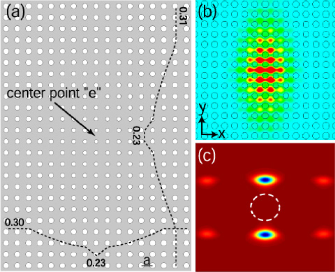
In Ref. Srinivasan and Painter (2002), high- PC cavities were designed by considering the Fourier space properties and symmetry of cavity modes. An important feature of these designs is their robustness, in that perturbations to the size and shape of individual holes do not deteriorate the significantly. Vertical radiation losses, which are characterized by the presence of power at in-plane momentum components () that lie within the light cone of the slab waveguide cladding, are reduced by choosing modes of a specific symmetry. In particular, the modes selected are those that are odd about mirror planes normal to the direction of the mode’s dominant Fourier components, eliminating the DC () part of the field. For the square lattice cavities studied in Ref. Srinivasan and Painter (2002), one such mode is a donor-type mode (labelled due to its symmetry) centered in the dielectric between two rows of air holes (point in Figure 1). Further improvements to both the in-plane and vertical loss are achieved by grading the lattice as shown in Figure 1(a). Figure 1(b)-(c) shows the magnetic field amplitude and Fourier transformed dominant electric field component for the resulting mode as calculated by finite-difference time-domain (FDTD) simulations. FDTD calculations predict for this mode, with a modal volume cubic half-wavelengths in air ( for refractive index , larger than original designs in Ref. Painter et al. (1999b)). Calculations show that the grade used in Figure 1(a) can be varied fairly significantly without degrading the to a value less than .
In order to measure the properties of the donor-type mode, graded square lattice PC cavities were fabricated in an active material consisting of five InAsP compressively-strained quantum wells, with peak spontaneous emission at 1285 nm. The details of the epitaxial growth and some of the important properties of the materials system are reported in Ref. Hwang et al. (1998). The creation of the 2D PC membrane is accomplished through a number of steps, including electron-beam lithography, pattern transfer to a SiO2 mask using an inductively coupled plasma reactive ion etch (ICP/RIE), and a high-temperature ( C) Ar-Cl2 ICP/RIE etch through the active material into a sacrificial InP layer. The sample is undercut by removing the InP layer with a HCl:H2O (4:1) solution leaving a 252 nm thick free-standing membrane; scanning electron micrographs (SEMs) of the graded lattice cavity are shown in Figure 2. Each cavity consisted of a total of 32 rows and 25 columns of air holes, with a lattice spacing of , , , or nm (chosen for m emission to be close to the normalized frequency of the mode, ), for total cavity dimensions on the order of m. The designed grade produces holes with radii between - nm. As will be described elsewhere, the fabrication was optimized to produce smooth vertical sidewalls in the holes, and to obtain small air holes, both of which were limitations of previous PC cavity workPainter et al. (1999b).
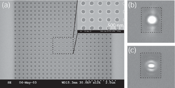
Devices are optically pumped (typically with a ns pulse width and ns period) at room temperature with a semiconductor laser at nm through a 20X objective lens, also used to collect emitted photoluminescence (PL) into an optical spectrum analyzer (OSA). We initially pump the cavities with a broad pump beam (see Figure 2(b), area ) for two reasons: (i) the broad pump beam covers a significant portion of the cavity area, so that after diffusion of carriers, the majority of the cavity should be pumped and therefore non-absorbing, and (ii) use of a broad pump beam limits the effects of thermal broadening, which, as discussed below, are significant for focused pump beams. A typical L-L (light-in vs. light-out) curve using the broad pump beam condition is shown in Figure 3(a), where the power in the laser line is taken over a 10 nm bandwidth about the laser wavelength of nm. In addition, the off-resonance background emission at nm was measured over a similar 10 nm bandwidth. For low pump powers ( W), the off-resonance emission and resonant wavelength emission linearly increase with pump power and are essentially identical in level, i.e., no resonance feature is observed. Above 300 W, we just begin to see a resonance peak in the spectrum and a characteristic super-linear transition from below threshold to above threshold follows. In order to estimate the position of threshold we extrapolate back the L-L curve from above threshold (Fig. 3(b)), giving an approximate threshold pump level of W. A plot of the off-resonance emission (Fig. 3(c)) shows a (weak) slope change around W giving a similar value for the estimated threshold value. The slope change in the laser line versus pump power is initially a result of the material becoming transparent (more photons being radiated as opposed to being absorbed), and is then due to an increase in the stimulated rate of emission into the cavity mode as the lasing threshold is crossed, increasing the radiative efficiency into the cavity mode due to the presence of non-radiative carrier recombination and spontaneous emission into other modes. The kink in the off-resonance background emission L-L curve can be attributed to the clamping of the carrier density (gain) in the region of the cavity mode and consequent saturation of the off-resonance (non-lasing modes’) emission. The background emission continues to increase after crossing threshold (rather than completely saturating) as a result of the pumping of areas which are outside of the cavity mode volume and thus not affected by the gain clamping (non-equilibrium carrier distributionsSlusher (1994) may also play a role).
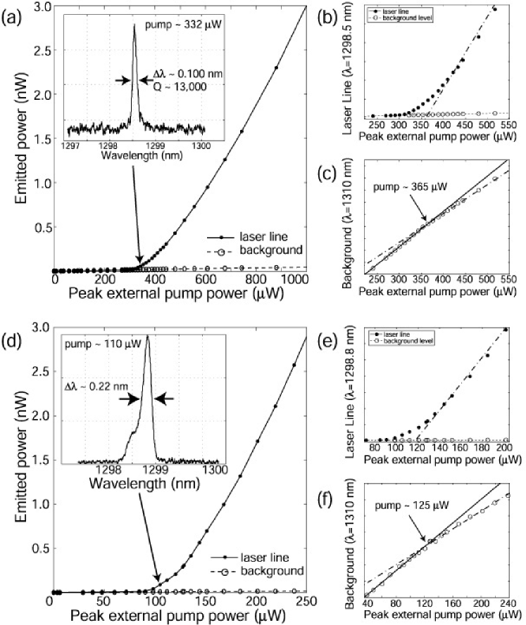
In order to estimate the cold cavity value of the PC microcavity mode we measured the linewidth of the resonance in the PL around threshold. The full-width half-maximum (FWHM) linewidth narrows from nm (at the lowest pump level we could accurately measure the linewidth, W) down to nm at threshold. A simple steady state rate equation modelAgrawal and Dutta (1993) of the cavity photon and excited state populations estimates the threshold pump level (with this beam size) to be W for in this quantum well active material, close to the experimentally measured value. In this model the transparency carrier density occurs within of the threshold carrier density for cavity modes with . A PL spectrum (Fig. 3(a), inset) for this device with the broad pump conditions, measured soon after detection of a resonance feature in the spectrum and below the estimated threshold level by about , shows a resonance linewidth nm, corresponding to a best estimate of the cold cavity . Above threshold we do not see further linewidth narrowing due to the resolution limit of the scanning monochromator ( nm) used, as well as the presence of thermal broadening of the emission line during the pump pulse (this may also be partially due to incomplete saturation of the carrier densitySlusher (1994)).
By using a more tightly focused beam (see Figure 2(c), area m2), the lasing threshold is considerably reduced. In Figures 3(d)-(f), we plot the L-L curve for the laser line and off-resonance background emission using such a pump beam. The plots are qualitatively similar to those for the diffuse pump beam; we begin to see a resonance feature when the pump power exceeds 95 W. Estimates for the threshold pump power from the laser line curve and off-resonance background emission are 120 W and 125 W, respectively. The reduction in lasing threshold from the broad pump beam to the focused pump beam follows a nearly linear scale with the area of the pump beam. Through further optimization of the pump beam, lasers with thresholds as low as W have been observed. From the sub-threshold spectrum shown in the inset of Figure 3(d) it is readily apparent that the lineshape has thermally broadened (the measured linewidth is now nm), as evidenced by its asymmetric shape on the short wavelength side. To reduce the effects of this thermal broadening, the duty cycle can be decreased to (1 s period and 10 ns pulse width), resulting in a less asymmetric resonance and sub-threshold linewidth of approximately nm. Conversely, we have also increased the duty cycle to (1 s period and 250 ns pulse width) and still observe lasing; heating in the membrane precludes lasing at even higher duty cycles.
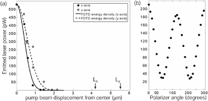
To determine whether the laser mode described above is indeed the localized mode of Figure 1, we have measured polarized intensity in the far-field as well as the sensitivity of the emitted laser power to pump position. The measurements show the mode to be predominantly polarized along the -axis (Fig. 4(b)) of the cavity, consistent with FDTD results, and eliminating the possibility that the mode is of the other potential symmetry supported by the cavity Srinivasan and Painter (2002). Furthermore, the lasing mode discussed above is the longest wavelength mode observed in the devices tested (higher frequency resonances are observed in some detuned devices), suggesting that it is the fundamental mode shown in Figure 1(b), and not a higher order version of it. In Figure 4(a) we show measurements of the emitted laser power as a function of the pump beam position (taken to be the center of the beam) relative to the center of the cavity (uncertainty in the pump position is m). The measurements indicate the mode is highly localized within the center of the cavity, consistent with simulations.
In summary, we have observed linewidths of nm, corresponding to a cavity of , in sub-threshold measurements of graded square lattice photonic crystal microcavity lasers fabricated in an InAsP/InGaAsP multi-quantum well membrane. In addition, lasing is seen at threshold peak external pump powers as low as 100 W. Measurements of the emitted power as a function of pump position show the mode to be strongly localized and give an estimate of the modal localization that is consistent with FDTD results. This realization of a high , small mode volume microcavity is an important step in demonstrating the potential of PC microcavities for use in optoelectronics and quantum optics.
K. Srinivasan thanks the Hertz Foundation for its financial support.
References
- Painter et al. (1999a) O. Painter, J. Vučković, and A. Scherer, J. Opt. Soc. Am. B 16(2), 275 (1999a).
- Painter et al. (1999b) O. Painter, R. K. Lee, A. Yariv, A. Scherer, J. D. O’Brien, P. D. Dapkus, and I. Kim, Science 284, 1819 (1999b).
- Vučković et al. (2002) J. Vučković, M. Lončar, H. Mabuchi, and A. Scherer, Phys. Rev. E 65(1) (2002).
- Srinivasan and Painter (2002) K. Srinivasan and O. Painter, Opt. Express 10(15), 670 (2002).
- Ryu et al. (2002) H.-Y. Ryu, S.-H. Kim, H.-G. Park, J.-K. Hwang, Y.-H. Lee, and J.-S. Kim, Appl. Phys. Lett. 80(21), 3883 (2002).
- Lončar et al. (2002) M. Lončar, T. Yoshie, P. Gogna, and Y. Qiu, Appl. Phys. Lett. 81(15), 2680 (2002).
- Yoshie et al. (2001) T. Yoshie, J. Vučković, A. Scherer, H. Chen, and D. Deppe, Appl. Phys. Lett. 79(26), 4289 (2001).
- Khitrova et al. (1999) G. Khitrova, H. M. Gibbs, F. Jahnke, M. Kira, and S. W. Koch, Rev. Mod. Phys. 71(5), 1591 (1999).
- Vernooy et al. (1998) D. W. Vernooy, A. Furasawa, N. P. Georgiades, V. S. Ilchenko, and H. J. Kimble, Phys. Rev. A 57(4), R2293 (1998).
- Michler et al. (2000) P. Michler, A. Kiraz, C. Becher, W. Schoenfeld, P. Petroff, L. Zhang, E. Hu, and A. Imomoglu, Science 290, 2282 (2000).
- Santori et al. (2001) C. Santori, M. Pelton, G. Solomon, Y. Dale, and Y. Yamamoto, Phys. Rev. Lett. 86(8), 1502 (2001).
- Spillane et al. (2002) S. M. Spillane, T. J. Kippenberg, and K. J. Vahala, Nature 415, 621 (2002).
- Gayral et al. (1999) B. Gayral, J. M. Gérard, A. Lematre, C. Dupuis, L. Manin, and J. L. Pelouard, Appl. Phys. Lett. 75(13), 1908 (1999).
- Gérard et al. (1998) J. M. Gérard, B. Sermage, B. Gayral, B. Legrand, E. Costard, and V. Thierry-Mieg, Phys. Rev. Lett. 81(5), 1110 (1998).
- Reese et al. (2001) C. Reese, B. Gayral, B. D. Gerardot, A. Imamoglu, P. M. Petroff, and E. Hu, J. Vac. S. Tech. B 19(6), 2749 (2001).
- Hwang et al. (1998) W.-Y. Hwang, J. Baillargeon, S. N. G. Chu, P. F. Sciortino, and A. Y. Cho, J. Vac. S. Tech. B 16(3), 1422 (1998).
- Slusher (1994) R. E. Slusher, Semiconductor Science and Technology 9(11), 2025 (1994).
- Agrawal and Dutta (1993) G. P. Agrawal and N. K. Dutta, Semiconductor Lasers (Van Nostrand Reinhold, New York, NY, 1993).