Negative Group Delay and Superluminal Propagation: An Electronic Circuit Approach
Abstract
We present a simple electronic circuit which provides negative group delays for band-limited, base-band pulses. It is shown that large time advancement comparable to the pulse width can be achieved with appropriate cascading of negative-delay circuits but eventually the out-of-band gain limits the number of cascading. The relations to superluminality and causality are also discussed.
Index Terms:
negative group delay, superluminal propagation, group velocity, filter, causalityI Introduction
Brillouin and Sommerfeld showed that in the region of anomalous dispersion, which is inside of the absorption band, the group velocity can exceed , the light speed in a vacuum, or even be negative [1, 2]. Recently, it was shown that for a gain medium, superluminal propagation is possible at the outside of the gain resonance. Superluminal effects are also predicted in terms of quantum tunneling or evanescent waves [3, 4, 5]. Superluminal group velocities have been confirmed experimentally in various systems, and most controversies over this counterintuitive phenomenon have settled down. However, there seem a several questions remain open; for example, “How far we can speed up the wave packets,” “Is it really nothing to do with information transmission,” “What kind of applications are possible,” and so on. In this paper we will try to solve some of these problems by utilizing a simple circuit model for negative group delays.
Negative delay in lumped systems such as electronic circuits is very helpful to understand various aspects of superluminal group velocity. Mitchell and Chiao [6, 7] constructed a bandpass amplifier with an resonator and an operational amplifier. An arbitrary waveform generator is used to generate a gaussian pulse by which a carrier is modulated. The circuit basically emulates an optical gain medium which shows anomalous dispersion in off-resonant region. Wang et al. [8] extended this circuit by using two resonators which correspond to the two Raman gain lines [9, 10]. At the middle of two gain peaks the frequency dependence of amplitude response is compensated and the pulse distortion can be minimized.
The present authors [11] used an operational amplifier with an feedback circuit. It provides negative delays for baseband pulses. In previous experiments, optical or electronic, a carrier frequency () is modulated by a pulse which varies slowly compared with the carrier oscillation and the displacement of the envelopes is measured. Without carriers (), the system becomes much more simple. The amplitude response symmetric with respect to zero frequency is helpful to reduce the distortion. The baseband pulse is simply derived from a rectangular pulse generator and a series of lowpass filters.
The time constants can easily be set at the order of seconds and we can actually observe that the output LED (light-emitting diode) is lit earlier than the input LED. In addition to the usefulness as a demonstration tool, this circuit turned out to be very convenient to look into the essentials of negative group delays and superluminal propagation because of its simplicity.
In this paper we exploit the circuit model in order to investigate some of the fundamental problems. First we discuss the relation between negative group delay and superluminarity, and then the approximate realization of (positive and negative) delays by lumped systems. Then we consider the spectral condition imposed on input pulses and describe the design of lowpass filters for pulse preparation. Next in order to increase the advancement, a number of negative delay circuits are cascaded. We find that an advancement as large as the pulse width is possible but the slow increase of the advancement and the exponential increase of out-of-band gain almost prohibit the achievement of further advancements. Finally by regarding our system as a communication channel, we discuss the causality in lumped systems.
II Negative delay and superluminal propagation
The group velocity in a dispersive medium is defined as
| (1) |
where the wavenumber is a function of frequency . It corresponds to the propagation speed of an envelope of signal whose spectrum is limited within a short interval containing .
Similarly the group delay is defined as
| (2) |
where represents the frequency-dependent phase shift. It corresponds to the temporal shift of the envelope of the band-limited signal passing through a system. For a medium with length , the phase shift is given by and we have
| (3) |
These two quantities seem almost identical, but the group delay is a more general concept because it can be defined even for a lumped system. The lumped system is a system whose size is much smaller than the wavelength of interest. Neglecting the propagation effects, the behavior of the system can be described by a set of ordinary differential equations with respect to time. For distributed systems, on the other hand, the spatio-temporal partial differential equation must be used.
The relation between negative group delays and superluminality can easily be understood when we consider a system consisting with a vacuum path (length ) and a lumped system (delay ) which is located at the end of the path. The total time required for a pulse to pass through the system is
| (4) |
The corresponding velocity satisfies the relation:
| (5) |
For (positive delay), is smaller than . For (negative delay), there are two cases. In the case , is larger than (superluminal in a narrow sense), while in the case , becomes negative (negative group velocity). In the latter case the contribution of the lumped part dominates that of the free propagation path.
Normally the superluminality has been considered as a propagation effect. But in many cases, it seems more appropriate to discuss in term of the negative group delay for a lumped system. Let us take experimental parameters from [9], in which the negative delay of was observed. We note that the pulse length is much longer than the cell length . Therefore we can safely use the lumped approximation. Since we can eliminate the carrier frequency by the slowly-varying envelope approximation, the wavelength of light () will not come into play any more.
It should be stressed that the cases where the second term in Eqs. (4) or (5), which is positive or negative, dominates the first term are very likely. For typical atomic experiments, the bandwidth , which is of the order of MHz to GHz, roughly determines advancement as , to , while the passage time is less than the order of. Forcible assignment of a velocity to such cases, in the above example, would have caused some confusions.
III Group delays – ideal and approximate
III-A Mathematical representation
A mathematical representation for ideal delays can be written as
| (6) |
where is the impulse response of the system and is the delay time. Its Fourier transform is given by
| (7) |
with
| (8) |
For (positive delay), the impulse response is causal, i.e., it is zero for . The positive delay can be realized easily, if you have an appropriate space (). But there is no way to make ideal, unconditional negative delays, because is non-causal in this case.
III-B Building blocks
It should be noted that no lumped systems () can produce ideal positive or negative delays. From now on let us consider how to make approximate delays with lumped systems. The amplitude and the phase of the ideal response function are
| (9) | |||||
| (10) |
In [11], we used a circuit having a transfer function
| (11) |
by which negative delay is provided for baseband pulses (). Here we will examine several transfer functions which can be realized with an operational amplifier and a few passive components.
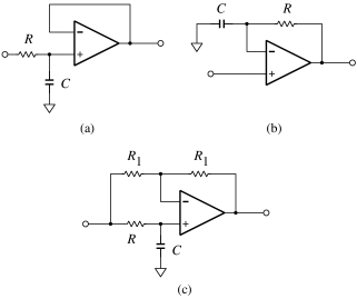
First, we consider a function with a single pole:
| (12) | |||||
| (13) | |||||
| (14) |
The stability condition that all the poles reside in the upper half plane requires , therefore, only positive delays can be achieved with this type of transfer function. An example of circuit is shown in Fig. 1(a). Only in the region , the amplitude response is flat and the phase response is linear. The circuit works only for band-limited signals.
Secondly, we will check a function with a single zero:
| (15) | |||||
| (16) | |||||
| (17) |
In this case, no sign restrictions are imposed on , therefore, both positive and negative delays can be realized; . A circuit for () is shown in Fig. 1(b). Perhaps this is the most simple circuit which provides negative delay. Again it works only in the region . Even worse is the rising of gain at the outside of the band. We can also construct a positive delay circuit utilizing the relation .
By observing the sign restrictions for and , we notice that an asymmetry between the positive and negative delays exists even in lumped systems.
Another interesting transfer function is
| (18) | |||||
| (19) | |||||
| (20) |
which can be realized by the circuit shown in Fig. 1(c). This circuit is called the all-pass filter. The phase function is the same as the above cases aside from the factor 2, but the amplitude response in independent of the frequency as in the case of ideal delay. The stability condition implies , therefore, only positive delays are possible.
IV Bandwidth and distortion
IV-A Bandwidth of negative delay circuit
It turned out that lumped circuits can provide a delay, positive or negative, only for a band-limited signal. From the approximate transfer function, , for negative delays, we have the imperfect amplitude and phase functions:

| (21) | |||||
| (22) |
which are plotted in Fig. 2. We see that the inputs must satisfy the spectral condition:
| (23) |
Otherwise the output waveform will be distorted due to the higher order terms in Eqs. (21) and (22). In electronic circuits, a rectangular pulse is most easily generated. But its spectrum has a long tail; . The tail must be suppressed with lowpass filters. The cutoff frequency must be smaller than .
IV-B Lowpass filter for pulse preparation
A simple method is to cascade suitable numbers of first-order lowpass filters, whose transfer function is represented by Eq. (14), as
| (24) |
where is a normalization parameter to keep the cutoff frequency constant. It is reduced as is increased. Otherwise, due to the decrease of bandwidth, the pulse width is broadened and the pulse height is reduced. For better low-pass characteristics, we can use Bessel filters [12, 13], whose transfer function is given by
| (25) |
where is the -th Bessel polynomials and the parameter is determined so that .


The effect of filtering is shown in Fig. 3 and Fig. 4. The initial, rectangular pulse is send to a series of filters, where represent the unit step function. As the order of the filter is increased, the high frequency tails are more suppressed and accordingly the waveform becomes smoother. Exceeding a few stages, the waveforms look very similar to each other. But the leading edge scales and the peak position is delayed. The delay, which is due to the phase transfer function of the lowpass filters, is unavoidable. We will see in Section VI that must be increased in order to attain large advancement. The pulse width approaches a value determined by the cutoff frequency , if the initial pulse width is smaller than .
From the way of preparation of input pulse with lowpass filters, we can interpret that the leading edge is shaped so as to be more predictable. The future can well be predicted, if enough restrictions are imposed on the pulse.
IV-C Gaussian pulse
The guassian pulse is widely used in negative delay or superluminal propagation experiments. It is because of the rapid tail-off of the spectrum and its mathematical simplicity. But there seems no natural implementation which generates a gaussian pulse. It is usually synthesized numerically and the calculated data is fed to a digital-to-analog converter. It should be noted that the ideal guassian pulse has a infinitely long leading edge. What we can generate practically is a truncated gaussian pulse:
| (26) |
where . A causal function is a unit step function or a smoothed version of it. This trancation necessarily introduces discontinuities for at and associates high frequency components. However small they may look like, eventually, they will be revealed by a negative delay circuit with advancement larger than . In order to reduce the effect of truncation, must be increased, which corresponds to the increase of in the pulse preparation with lowpass filters.
V Experiment
V-A Practical design
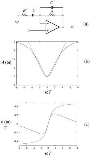
Figure 5(a) shows a practical circuit for negative delays [11]. The components are are added to the circuit of Fig. 1(b) in order to suppress the gain for higher frequency. Its transfer function can easily be derived. First, we see that
| (27) |
where , . If we assume a large gain of the operational amplifier, the virtual short condition, , holds and we have
| (28) | |||||
where . If and are satisfied, then the transfer function is approximated as near the origin (). Thanks to or , the maximum gain is limited by . The response functions for , are plotted in Figs. 5(b) and (c). The phase slope at the origin is almost conserved but the usable bandwidth is reduced.
V-B Experimental result
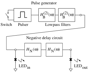
In Fig. 7, we show the overall block diagram for the negative delay experiment. The complete circuit diagram is presented in [11]. The pulse generator on the top is composed of a single-shot pulser and two 2nd-order Bessel filters. Triggered by the switch, a timer IC (ICM7555) generates a rectangular pulse with duration . The pulse is shaped by the filters. The cut-off frequency is chosen as , so that and can be considered to be constant and linear, respectively. is the time constant of the negative delay circuits.
Two negative delay circuits are cascaded for larger advancement. The circuit parameters are , , , .
The input and output terminals are monitored by LEDs. Their turn-on voltage is about .

The experimental result is shown in Fig. 8. The input and output waveforms are recorded with an oscilloscope. The time origin () is the moment when the switch is turned on or the rising edge of the initial rectangular pulse.
We see that the output pulse precedes the input pulse considerably (more than 20% of the pulse width). The slight distortion of the output waveform is caused by the non-ideal frequency dependence of and .
The observed advancement of agrees well with the expected value .
General purpose operational amplifiers (TL082) are used for low-pass filters and negative delay circuits. The time scale has been chosen so that we can directly observe the negative delay with two LEDs connected at the input and the output terminals. The whole experimental setup can be battery-operated and self-contained. If we want to observe the waveform, in stead of oscilloscopes, we can use two analog voltmeters (or circuit testers) to monitor the waveforms.
VI Cascading — for larger advancement
VI-A Normalized advancement
We have seen that in typical situations the advancement is fairly smaller than the pulse width . Typically the relative advancement only reaches to a few percents.
To see the reason, we consider a gaussian pulse and its Fourier transform . When it is passed through the negative delay circuit, the power is amplified owing to the rising amplitude response (16). We define the excess power gain as
| (30) |
which can be used as a measure of distortion. Now we have a relation between and the relative advancement ;
| (31) |
For example, if we allow , then the relative advancement is at most.
If we want to increase the advancement , for a given system, the bandwidth must be reduced, which results in the increase of pulse width and does not increase.
VI-B Degression of time constant
We will try to increase the relative advancement by cascading the negative group delay circuits in series. The transfer function for stages:
| (32) | |||||
| (33) | |||||
| (34) |
At first, we may expect that the total advancement increases in proportional to because the slope of at the origin increases as . But we should notice by looking at that the usable bandwidth is reduced as increased for fixed. In other words, for a given input pulse width , must be reduced as . Thus the total advancement scales as
| (35) |
It should be noted that the gain outside of the band is increases very rapidly. Spectral tails of the input pulse must be suppressed enough. Otherwise they could be amplified to distort the pulse shape. From the asymptotic forms of and , we see that the condition must be satisfied. Order of lowpass filters must be increased cooperatively. It is possible to increase the advancement as large as the pulse width or more, but the advancement increases very slowly; .
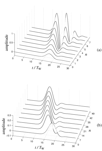
Fig. 9(a) represents a example of simple-minded cascading, where is kept constant. The waveforms are rapidly distorted as increased.
Fig. 9(b) shows the cascading, where is reduced as . The pulse shape is preserved fairly well. The input pulse is filtered with five 10-th order Bessel filters ().
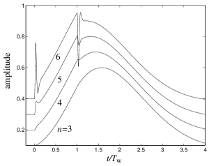
Figure 10 shows the case of . The input rectangular pulse is filtered by a 4-th order Bessel filter (). For cascading, scars of the initial pulse appear at and , and they become more prominent as increases.
VI-C Out-of-band gain
As we have seen, the out-of-band gain is the primary obstacle toward large advancement. In order to estimate how the gain increases we use a realistic transfer function (28), which has a finite maximum gain . For , , , we have
| (36) |
Such a huge gain will certainly induce instabilities. The noise level must also be suppressed. If we increase or to reduce , then the bandwidth is significantly reduced as seen in Fig. 5. For the reduced bandwidth, we have to increase the pulse width , which diminishes the relative advancement .
We see from this example, a large negative delay comparable to the pulse width is very hard to achieve or almost prohibitive. The allowable gain would be limited by system-dependent factors such as a performance of active devices, a threshold for instabilities, fluctuation due to quantum noise, and so on.
Again we notice the asymmetry between the negative and the positive delays. For positive delays, gain problem does not occur. In fact, the cascading of lowpass filters yields a large amount of delay without difficulty.
VII Discussion
VII-A Interference in the time domain
From the minimal transfer function, , for the negative delay, we see that in time domain the input-output relation can be written as
| (37) |
Here the two terms interfere constructively at the leading edge and destructively at the trailing edge. The addition of the time derivative to the original pulse results in the pulse forwarding.
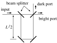
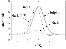
This time domain picture is useful to devise a new system which shows negative delays. The Mach-Zehnder interferometer shown in Fig. 11 is such an example. First we assume for the reflectivity of the beam splitters. The path difference is chosen so as to satisfy the condition , where is the wavelength, is the pulse width, and is the delay time due to the path difference. We can tune the path length so that the transmission for one port is unity. Then for the steady state, there appears no output at the other port (dark port) owing to the destructive interference.
For time dependent inputs, however, the cancellation is incomplete and the output corresponding to the time derivative of the amplitude appears at the dark port (see Fig. 12). If we superpose this output with the original waveform, we will have the advancement as shown in Eq. (37). The superposition can easily be provided by unbalancing the amplitude of each path. We set the reflectivity of the two beam splitters is slightly smaller than 50% : . Then the output of the dark port becomes
| (38) | |||||
and the advancement of is achieved. and are the envelope of the input field and the dark port field, respectively. The usable bandwidth of the system is , for which the darkness of the dark port is ensured.
This is an example of all-passive systems with negative delay. It should be noted that when we increase the advancement by decreasing , the transmission is decreased accordingly. It is also true for the superluminal propagation of evanescent waves and tunneling waves [4, 5].
This model convinces us that the negative group delay and the superluminal group velocity are the simple consequence of wave interference.
VII-B Causality and negative delay
It has been well recognized and confirmed in many ways that the front velocity is connected with the causality, and the causality has no direct connection with the group velocity. But one is still apt to connect the group velocity with the causality because many practical communication systems utilize pulse modulation to send information.
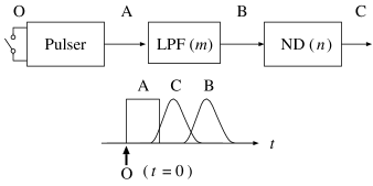
Let us examine our system shown in Fig. 13 in terms of causality. By pushing the switch (O), a rectangular pulse (A) is generated. Feeding it into the lowpass filter, a band-limited pulse (B) is prepared. Finally sending it through the negative delay circuit, an advanced pulse (C) is created. This would be a cause-effect chain in a casual sense. However the reversal of the chronological order between (B) and (C) causes the trouble for the naive picture. One may think that making use of this twist it is possible to send information to the past despite of the causality. Of course this is wrong.
First we should realize that in a strict sense all the pulses (A), (B), and (C) are causal to each other because they are the signals in a single lumped system. When an impulse is applied to a quiescent lumped system, then all parts respond instantaneously. Some of them look delayed, but they just started smoothly as (). All the pulse fronts share the time , when the switch is turned on (O). Therefore the above discussion on the order is totally pointless.
But one may still shelve the theory, which deals with the almost unseen signals just after , considering practical situation where the information is related to the peak position or the rising edge where a half of the pulse peak is reached. However, in order to generate a smooth pulse (B) which is acceptable to the negative delay circuit, we have to make a decision well in advance (before in this case) because of the delay caused by the lowpass filter. Once we miss the timing, the number of the lowpass filters must be reduced in order to catch up. But breaking the condition , the pulse cannot be forwarded any more and is distorted badly.
Let us regard the negative delay circuit of Fig. 13 as a communication channel. We assign three people, Alice, Bob, and Clare, on the sites (A), (B), and (C), respectively. Clare always finds a pulse before Bob does, i.e., she can always predict Bob’s pulse. But Bob has no control over his pulses; he cannot cancel a pulse initiated by Alice. The real sender of the pulse is not Bob, but Alice. Bob is just an observer standing at the sending site. This scenario tells us that comparing the input and the output pulses of superluminal channel is somewhat nonsense and that the real start point of the input pulse should be considered (See Sec. IV-C).
VIII Concluding remarks
The negative group delay is already utilized in many practical applications implicitly. Signals from slow sensors, such as a hotwire anemometer, are compensated by a differentiator with a transfer function . In PID (Proportional, Integral, and Derivative) controllers the derivative element (D) is used to predict the behavior of the system and to improve the dynamical response. When a capacitive load is connected to the output of an operational amplifier, an additional feedback loop with derivative element is used, which is called lead compensations. All these efforts are to compensate delays in a system as far as possible but the excessive use will result in instabilities or noise problems.
We have explored many aspects of negative delays and superluminality utilizing circuit models. The use of circuit model is very helpful because the choice of parameters are very flexible and many handy circuit-simulation softwares are available. Extension to nonlinear cases and to distributed systems [14] will be very interesting.
acknowledgments
One of the authors (MK) greatly appreciates stimulating and inspiring discussions with R. Chiao and all the participants of the mini program on Quantum Optics at the Institute of Theoretical Physics, University of California Santa Barbara. He also thanks K. Shimoda for informing about practical use of negative delay circuits.
References
- [1] L. Brillouin, Wave Propagation and Group Velocity. New York: Academic Press, 1960, pp. 113–137.
- [2] S. Chu and S. Wong, “Linear pulse propagation in an absorbing medium,” Phys. Rev. Lett., vol. 48, pp. 738–741, Mar. 1982.
- [3] R. Y. Chiao and A. M. Steinberg, “Tunneling times and superluminality” Prog. Opt., vol. XXXVII, pp. 345–405, 1997.
- [4] G. Enders and G. Nimtz, “On the superluminal barrier traversal,” J. Phys., vol. I2, pp. 1693–1698, Sep. 1992.
- [5] A. M. Steinberg, P. G. Kwiat, and R. Y. Chiao, “Measurement of the single-photon tunneling time,” Phys. Rev. Lett., vol. 71, pp. 708–711, Aug. 1993.
- [6] M. W. Mitchell and R. Y. Chiao, “Causality and negative group delays in a simple bandpass amplifier,” Am. J. Phys., vol. 66, pp. 14–19, Jan. 1998.
- [7] M. W. Mitchell and R. Y. Chiao, “Negative group delay and ‘fronts’ in a causal systems: An experiment with very low frequency bandpass amplifiers,” Phys. Lett., vol. A230, pp. 133–138, Jun. 1997.
- [8] H. Cao, A. Dogariu, and L. J. Wang, “Negative group delay and pulse compression in superluminal pulse propagation,” unpublished.
- [9] L. J. Wang, A. Kuzmich, and A. Dogariu, “Gain-assisted superluminal light propagation,” Nature, vol. 406, pp. 277–279, Jul. 2000.
- [10] A. Dogariu, A. Kuzmich, and L. J. Wang, “Transparent anomalous dispersion and superluminal light-pulse propagation at a negative group velocity,” Phys. Rev. A, vol. 63, pp. 053806-1–11, Apr. 2001.
- [11] T. Nakanishi, K. Sugiyama, and M. Kitano, “Demonstration of negative group delays in a simple electronic circuit,” Am. J. Phys., vol. 70, pp. 1117–1121, Nov. 2002.
- [12] U. Tietze and Ch. Schenk, Electronic Circuits. Verlin: Springer-Verlag, 1991, pp. 350–408.
- [13] P. Horowitz and W. Hill, The Art of Electronics, 2nd Ed. Cambridge: Cambridge University Press, 1989, pp. 175–284.
- [14] R. W. Ziolkowski, “Superluminal transmission of information through an electromagnetic metamaterial,” Phys. Rev. E, vol. 63, pp. 046604-1–13, Apr. 2001.