A single photoelectron transistor for quantum optical communications
Abstract
A single photoelectron can be trapped and its photoelectric charge detected by a source/drain channel in a transistor. Such a transistor photodetector can be useful for flagging the safe arrival of a photon in a quantum repeater. The electron trap can be photo-ionized and repeatedly reset for the arrival of successive individual photons. This single photoelectron transistor (SPT) operating at the = 1.3m tele-communication band, was demonstrated by using a windowed-gate double-quantum-well InGaAs/InAlAs/InP heterostructure that was designed to provide near-zero electron g-factor. The g-factor engineering allows selection rules that would convert a photon’s polarization to an electron spin polarization. The safe arrival of the photo-electric charge would trigger the commencement of the teleportation algorithm.
pacs:
85.35.Gv, 73.50.Pz, 85.35.Be, 78.67.DeQuantum information can take several different forms and it is beneficial to be able to convert among the different forms. One form is photon polarization, and another is electron spin polarization.
Photons are the most convenient medium for sharing quantum information between distant locations. Quantum key distribution Bennett92 has been demonstrated by sending photons through a conventional optical fiber up to distances over 80km Hiskett . As the distance increases, the secure data rate decreases, owing to photon loss. To expand the distance dramatically, it is necessary to realize a quantum repeater, that is based on quantum teleportation Bennett93 . A quantum repeater requires quantum information storage van Enk , and electron spin is a good candidate for such a quantum memory. We need to have a photodetector that converts from photon to electron, while transferring the quantum information from photon polarization to electron spin. This is sometimes called an entanglement preserving photodetector Vrijen . In addition, the photodetector must provide a trigger signal to flag the arrival of a photo-electric charge, and to commence the teleportation algorithm.
A Field Effect Transistor (FET), and a Single Electron Transistor (SET) based on quantum dots, can both function as sensitive electrometers that can detect a single trapped electric charge. Our goal is to safely trap a photoelectron, so that its spin state can then be monitored. In this paper we demonstrate the trapping and manipulation of individual photoelectrons, but we have not yet measured the trapped electron’s spin properties. Previous experiments have demonstrated interband photon absorption resulting in the trapping of photoholes; on self-assembled InAs quantum dots shields , or on DX centers kosaka02 , near an FET source/drain channel. These produce positive photoconductivity, that is fairly common. The trapping of photoelectrons is much more rarely observed, since it is accompanied by negative photoconductivity rose .
Several kinds of photon effects on SETs made on modulation-doped semiconductors have been reported. Photon assisted tunneling is the most common effect. The tunneling takes place between an island and source-drain reservoir blick98 ; blick95 , between two adjacent islands vaart , or between an inner island and an outer ring split into Landau levels by a magnetic field komiyama . In all these cases, the rather long photon wavelengths are controlled by the electron sub-band energy difference, rather than by the fundamental bandgap as in our experiments.
These types of single photon detectors should be distinguished from avalanche photo-diodes, where the single photon sensitivity arises from avalanche gain. In the FET and SET photodetectors, a single trapped electric charge can influence the current of millions of electrons in the source/drain channel. This is indeed the mechanism of “photoconductive gain” rose that is also sometimes called “secondary photoconductivity” rose . But this form of gain can also be considered as arising from transistor action. Thus the name ”single photoelectron transistor” (SPT) might be appropriate. Since the photoelectron is safely trapped, and is known to have a long spin lifetime in many semiconductors awschalom , it can then be interrogated to determine its spin state. The initial goal is to monitor the photo-electric charge in such a way as to not disturb its spin state. Ultimately the goal is to measure its spin state as well.
At least three requirements should be satisfied to make a photodetector for quantum repeaters: (1) The wavelength that should be in the 1.3m or 1.55m, the low-loss window of optical fibers. (2) The sign of the photoconductivity that should be negative, which means the trapped information carrier should be an electron instead of a hole. (3) The electron ge-factor, which should be small, to make the up-and-down electron spin states as indistinguishable as possible Vrijen . The 1st requirement suggests interband transition rather than intraband transition. The 2nd requirement suggests creation of a positively charged trap for an electron. The 3rd requirement is satisfied through ge-factor engineering kosaka01 ; kiselev02 .
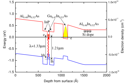
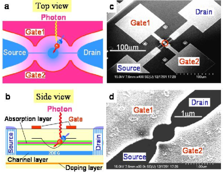
The single photoelectron transistor (SPT) that we present in this paper satisfies all of the above requirements. An InGaAs quantum well is used with a bandgap corresponding to = 1.3 m, as shown in Fig. 1. In Fig. 2 is shown the window-shaped circular gates that are negatively biased above the two-dimensional electron gas (2DEG), leaving behind a relatively positive central island. The InGaAs absorption layer, which has a ge-factor = –4.5 in the bulk, is sandwiched between InP cladding layers, of ge-factor = +1.2, to make the effective ge-factor in the absorption layer nearly zero. The measurements showed clear evidence for negative persistent photoconductivity steps. The abrupt drops in photoconductivity are strongly correlated with photon injection at the = 1.3 m wavelength, leading to the conclusion that the SPT detects a single photon by sensing the charge of a safely trapped photoelectron in the absorption quantum well.
The photo-absorption layer is located above the source/drain channel layer, and both are made of In0.53Ga0.47As, separated by a high electron barrier layer made of In0.52Al0.48As to prevent leakage. The source/drain channel layer is modulation doped and formed into a 1-dimensional electron gas (1DEG) channel whose conductance is sensitive to the charge state of the island in the absorption layer above it. All layers were grown by gas-source molecular beam epitaxy on semi-insulating InP, and consisted of a nominally undoped InP buffer layer 100nm thick; an i-In0.52Al0.48As buffer 1000nm thick; a Si-doped (5 1017/cm3) n-In0.52Al0.48As doping layer 10nm thick; an i-In0.52Al0.48As lower spacer layer 30nm thick; an i-In0.53Ga0.47As channel layer 10nm thick; an i-In0.52Al0.48As barrier layer 20nm thick; an i-InP cladding layer 10nm thick; an i-In0.53Ga0.47As absorption layer 4.5nm thick; an i-InP cladding layer 10nm thick; and an i-In0.52Al0.48As capping layer 60nm thick. The modulation-doped double-quantum well structure creates a 2DEG in the lower quantum well that is shaped into a 1DEG channel by the two split gates. The gates surround a circular window, 1 m in diameter, that masks out unnecessary light exposure, and fixes the potential at the edges surrounding of the window. The Schottky gates, Al/Pt/Au, are fabricated using electron-beam lithography and electron-gun evaporation. The source/drain ohmic contacts are made of AuGe/Ni/Au. Scanning Electron Microscope pictures of the whole device and the window gates are shown in Figs. 2c and 2d, respectively. The energy band diagram at zero bias, simulated by one-dimensional Poisson/Schrödinger equation, is shown in Fig. 1.
The sample is illuminated by monochromatic light through a large-core glass fiber, that is carefully shielded to block any photons from the outer jacket. The light is created by a tungsten lamp and then filtered by a monochromator, a long-pass filter passing wavelengths >1000nm, and a 30dB neutral density filter. The optical power at the end of the fiber is measured by a InGaAs detector. The illumination area in the plane of the device is about 5mm in diameter owing to light diffraction from the end of the fiber. Given the small device active area of 7.9 109 cm2, defined by the 1 m diameter gate window, we estimate the actual light power in the active area to be 2.8 10-8 times smaller than the total power (assuming a Gaussian profile). The incident photon number is estimated by multiplying this scaling factor by the measured power divided by the photon energy.
By applying a negative voltage to the split window gates, the source/drain current through the channel layer is pinched off. Simultaneously, the applied negative voltage creates a two-dimensional potential minimum in the window at the absorption layer. This is because the surface Fermi level in the circular area is pinned by the extrinsic surface states chou . The electric field in the electrostatic potential well can separate an electron-hole pair created by a photon. The electron is attracted to the potential minimum at on center, and the hole is attracted to the negative gates as schematically shown in Fig. 2b.
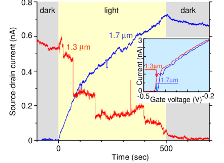
The source/drain current is measured at a constant voltage drop (Vsd) of 0.5mV, at a temperature of 4.2 K. The interesting property of these photodetectors is that = 1.77 m light produces positive photoconductivity effectively doping the channel, and = 1.3 m light produces negative photoconductivity. We attribute the channel doping by = 1.77 m light to be due to photo-ionization of donors in the n-InAlAs doping layer. As a normal practice, we initially prepare the photodetectors for use by means of a deep soak in = 1.77 m light, to fully ionize the donors and to populate the source/drain channel. The pinch-off behavior in the source-drain conductance (Isd-Vg curve) is shown in the inset of Fig. 3. The left-most I-V curve in that inset corresponds to full modulation doping after a deep soak in = 1.77 m light.
After the deep soak in = 1.77 m light to produce full channel doping, the gate voltage is adjusted for a current around 0.6nAmp. The device is then exposed to a photon flux at a wavelength of = 1.3 m (red curve labeled 1.3 m in Fig. 3). The photon exposure at = 1.3 m causes current to drop inexorably, step-by-step, except for occasional upward spikes. Thus as a result of trapped photoelectrons, the current is again pinched off, and the Isd-Vg curve was shifted toward positive gate voltages as shown in the right-most curve of the inset in Fig. 3. At this pinch-off condition, if the device was again exposed to = 1.77 m, the channel current would be restored (blue curve labeled 1.7 m in Fig. 3). The incident photon rate in the active window area for both wavelengths is about 100 photons/s. Since the absorptivity in the absorption layer is about 1%, on average 1 photon/sec is absorbed in the window area. Thus the quantum efficiency for producing negative steps is estimated to be 1%.
The current drop for = 1.3 m means that net negative charge
is trapped near the source/drain channel. The exposure to = 1.77 m photons is energetically able to cause only photo-ionization, because
the photon energy is smaller than any bandgaps.
Detailed examination of the spectral dependence is not straightforward since
the channel conductance depends on the starting bias, and the full history
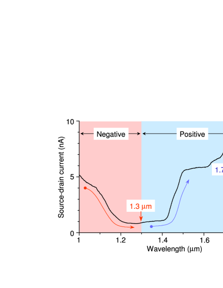
of spectral exposure. In Fig. 4 we start with an unpinched
channel, and sweep wavelength starting from = 1 m up to = 1.8 m over an 80second time period. First the current
monotonically decreases with increasing wavelength, corresponding to trapped
electrons, with no further decrease at around = 1.3 m, the
bandgap of the InGaAs quantum wells. Negative trapped charge at wavelengths
shorter than = 1.3 m is caused by photon absorption in the
absorption layer or the channel layer. The photoelectrons in the conducting
channel are mobile, and thus cannot contribute to trapped charge. Thus the
negative steps must originate from photoelectrons produced in the absorption
layer.
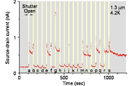
By having an incomplete initial soak in = 1.77 m radiation, we can control the pinch off voltage in between -0.5V and +0.1V. Now, when the pinch-off voltage is set to nearly zero, the = 1.3 m photocurrent still shows steps but they are equally likely to be either positive or negative. The incomplete photo-ionization of donors in the initial state allows a balance between electron trapping and photo-ionization. To make this phenomenon clear, we periodically opened the optical shutter for 10 seconds in every 50 seconds, maintaining the SPT in a balanced condition biased at 0 Volts. The resulting current pulses are shown in Fig. 5. The optical shutter is open during the time slots labeled a, b, c, etc., and closed during the intervening periods. Successive optical pulses usually produced either electron trapping or photo-ionization, alternating, depending on the previous state. Sometimes multiple optical pulses were required before the state would alternate. Within the 10sec optical pulse there might be a transient thermal response, especially in time slot g; but that returned to either of the two alternating states after the optical pulse. The photon number absorbed in the window area is 30 on average within the 10sec pulse. The estimated quantum efficiency is consistent with that in Fig. 3.
The switching behavior in Fig. 5 is due to photoelectron trapping/de-trapping located either in; (a) the shallow circular potential well between the window gates in the absorption layer, or (b) at donor sites. In case (b) the donors that could contribute to trapping/de-trapping are the residual donors in the absorption layer rather than those in the modulation doped layer. The modulation-doped donors, which are located far below the channel, would only produce a smooth increase in conductivity by photo-ionization as was seen in Fig. 3 for = 1.77 m light. In either case (a) or (b), there are two possible mechanisms for the positive steps in Fig. 5; photo-ionization of the trapped electron, or annihilation of the trapped electron by injected holes. The photo-ionization mechanism would require a specific photo-ionization cross-section to be consistent with the rough equality between trapping and de-trapping rates. On the other hand, annihilation by photo-holes would require a hole trapping rate that is roughly coincident with the electron trapping rate. Such an adjustment may have been made by the adjustment of potential wells through the pinch-off voltage requirement of Fig. 5.
In conclusion, we have trapped and safely stored single photoelectrons in a window-gate double-quantum-well transistor structure. This Single Photoelectron Transistor detector satisfies three key requirements for a quantum repeater photo-detector. It has a wavelength suitable for optical fibers, it safely traps and detects a single photoelectron, and the ge-factors can be designed to satisfy the requirements for an entanglement preserving photo-detector. The wavelength could be shifted to = 1.55 m, which is more preferable, by using strain engineered substrates [15]. The Single Photoelectron Transistor announces the arrival of the photoelectric charge, without disturbing the transfer of quantum information from photon polarization to the electron spin state. We have yet to prove the entanglement transfer, but we believe such a demonstration will be a breakthrough for realizing long-distance quantum key distribution or long distance teleportation.
The project is sponsored by the Defense Advanced Research Projects Agency & Army Research Office Nos. MDA972-99-1-0017 and DAAD19-00-1-0172. The content of the information does not necessarily reflect the position or the policy of the government, and no official endorsement should be inferred.
References
- (1) C.H. Bennett, F. Bessette, G. Brassard, L. Salvail, and J. Smolin, J. Cryptology 5, 3 (1992).
- (2) A.P. Hiskett, G. Bonfrate, G.S. Buller, and P.D. Townsend, J. Modern Optics 48, 1957, (2001).
- (3) C.H. Bennett, G. Brassard, C. Crepeau, R. Jozsa, A. Peres, and W.K. Wootters, Phys. Rev. Lett. 70, 1895 (1993).
- (4) S.J. van Enk, J.I. Cirac and P. Zoller, Phys. Rev. Lett. 78, 4293 (1997).
- (5) R. Vrijen and E. Yablonovitch, Physica E 10, 569 (2001).
- (6) A. J. Shields et al., Appl. Phys. Lett. 76, 3673 (2000).
- (7) H. Kosaka et al., Phys. Rev. B 65, R201307 (2002).
- (8) A. Rose, Concepts in Photoconductivity and Allied Problems (Krieger Publishing Co. Huntington New York, 1978).
- (9) R.H. Blick, V. Gudmundsson, R.J. Haug, K. von Klitzing, and K. Eberl, Phys. Rev. B 57, R12685 (1998).
- (10) R.H. Blick, R.J. Haug, D.W. van der Weide, K. von Klitzing, and K. Ebert, Appl. Phys. Lett. 67, 3924 (1995).
- (11) N.C. van der Vaart et al., Phys. Rev. B 55, 9746 (1997).
- (12) S. Komiyama, O. Astafiev, V. Antonov, T. Kutsuwa, and H. Hirai, Nature 403, 405 (2000).
- (13) D.D. Awschalom and J.M. Kikkawa, Physics Today 52, 33 (1999).
- (14) H. Kosaka, A.A. Kiselev, F.A. Baron, K-W. Kim, and E. Yablonovitch, Electron. Lett. 37, 464 (2001).
- (15) A.A. Kiselev, K.W. Kim, and E. Yablonovitch, Appl. Phys. Lett. 80, 2857 (2002).
- (16) W.Y. Chou, G.S. Chang, W.C. Hwang, and J.S. Hwang, J. Appl. Phys. 83, 3690 (1998).