Error Rate of the Kane Quantum Computer CNOT Gate in the Presence of Dephasing
Abstract
We study the error rate of CNOT operations in the Kane solid state quantum computer architecture [1]. A spin Hamiltonian is used to describe the system. Dephasing is included as exponential decay of the off diagonal elements of the system’s density matrix. Using available spin echo decay data, the CNOT error rate is estimated at approximately .
1 Introduction
Existing classical computers manipulate bits that can be exclusively or . Quantum computers manipulate two level quantum systems called qubits that can be arbitrary superpositions of and . While the idea of a quantum computer was first suggested by Benioff and Feynman in the early 80s [2, 3], the first quantum algorithm that could solve an interesting real world problem faster than it’s classical equivalent was published by Shor in [4]. Shor’s algorithm factorizes integers with the number of steps growing polynomially in the number of digits whereas the best known classical algorithm grows exponentially. A significant milestone in the quest to build a quantum computer was the construction of a 7 qubit liquid NMR implementation of Shor’s algorithm designed to factorize 15 [5]. Unfortunately, the liquid NMR approach is not expected to work beyond a few tens of qubits [6].
Many different technologies are being researched in the hope of producing a scalable quantum computer. A sample of the diverse proposals can be found in [1, 7, 8, 9, 10, 11]. In Kane’s solid state proposal [1, 12], the nuclear spins of single 31P dopant atoms in 28Si are used as qubits. This approach aims to take maximum advantage of the industry expertise acquired during the last 50 years of conventional semiconductor electronics.
In this paper we study the error rate of CNOT operations in the Kane quantum computer. Initial simulations were carried out without dephasing to enable the pulse profiles of the controlling electrodes to be optimized [13]. The lowest error rate achieved in the absence of dephasing was . When a physically reasonable level of dephasing was included in the simulation, the error rate increased to approximately . While theoretical estimates of the error rate required for fault tolerant computation are of order [14], numerical simulations by Zalka suggest an error rate of or higher may be tolerable [15]. Further work is required to determine the maximum allowed error rate in the Kane architecture.
This paper is organized as follows. In section 2 the physical architecture of the Kane quantum computer is described. In section 3 the process of performing a CNOT operation in the Kane architecture is presented with emphasis on achieving the lowest possible error rate in the absence of dephasing. Further details of this process can be found in [16]. In section 4 our model of dephasing is described and its effect on the error rate of the CNOT gate. In section 5 we conclude with a discussion of the implications of our estimate of the likely minimum error rate of the Kane CNOT gate.
2 The Kane Quantum Computer
The 31P in 28Si system is thought to be well suited to use as a qubit due to it’s long relaxation (T1) and dephasing (T2) times. Both times only have meaning when the system is in a steady magnetic field. Assuming the field is parallel with the z-axis, the relaxation time refers to the time taken for of the spins in the sample to spontaneously flip whereas the dephasing time refers to the time taken for the and components of a single spin to decay by a factor of . In natural silicon containing 4.7% 29Si, relaxation times T1 in excess 1 hour have been observed for the donor electron at T=1.25K and B0.3T [17]. The nuclear relaxation time has been estimated at over 80 hours in similar conditions [18]. The donor electron dephasing time T2 in enriched 28Si containing 29Si [19] has been measured at T=1.4K to be 0.5ms [20]. At the time of writing, no experimental data relating to the nuclear dephasing time has been obtained to the authors’ knowledge.
The phosphorous donor electrons are used primarily to mediate interactions between neighboring nuclear qubits. As such, they are polarized to remove their spin degree of freedom from the system. This can be achieved by maintaining a steady Bz=2T at around T=4K [16]. To take advantage of the long T1 and T2 times discussed in the previous paragraph, the operating temperature will more likely need to be 1K. Techniques for relaxing the high field and low temperature requirements such as spin refrigeration are under investigation [12].
In the Kane architecture, qubits are arranged in a single line. Control is achieved via electrodes above and between each qubit and a global transverse oscillating field of magnitude T (Fig. 1).
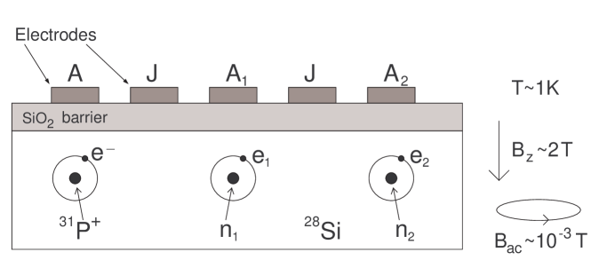
To selectively manipulate a single qubit, the A-electrode above it is biased. A positive/negative bias draws/drives the donor electron away from the nucleus reducing the magnitude of the interaction between the electron and nuclear spins. This in turn reduces the energy difference between nuclear spin up () and down () allowing this transition to be brought into resonance with a globally applied oscillating magnetic field. Depending on the timing of the A-electrode bias, the qubit can be rotated into an arbitrary superposition . Clearly this scheme also allows arbitrary combinations of individual qubits to be simultaneously and independently manipulated.
Interactions between neighboring qubits are governed by the J-electrodes. A positive bias encourages greater overlap of the donor electron wave functions leading to indirect coupling of their associated nuclei. In analogy to the single qubit case, this allows two qubit transitions to be performed selectively between arbitrary neighbors. A discussion of the electrode pulses required to implement a CNOT gate is given in the next section.
3 The CNOT Gate on a Kane QC
Performing a CNOT operation on a Kane QC is an involved process described in detail in [16]. Given the high field (2T) and low temperature (1K) operating conditions, we can model the behavior of the system with a spin Hamiltonian. Only two qubits are required to perform a CNOT operations so for the remainder of the paper we will restrict our attention to a computer with just two qubits. The basic notation is shown in (Fig. 1). Furthermore, let , , and where is the identity matrix, is the usual Pauli matrix and denotes the matrix outer product. With these definitions the meaning of terms such as and should be self evident.
Let be the g-factor for the phosphorus nucleus, the nuclear magneton and the Bohr magneton. The Hamiltonian can be broken into three parts
| (1) |
The Zeeman interactions terms are contained in
| (2) |
The contact hyperfine and exchange interaction terms, both of which can be modified via the electrode potentials are
| (3) |
where , is the magnitude of the wavefunction of donor electron at phosphorous nucleus , and depends on the overlap of the two donor electron wave functions. The dependance of these quantities on their associated electrode voltages is a subject of ongoing research [21, 22, 23]. In this paper the hyperfine and exchange interaction magnitudes and will frequently be discussed as though directly manipulable.
The last part of the Hamiltonian contains the coupling to the global oscillating field .
| (4) | |||||
Using the above definitions, only the quantities , and need to be manipulated to perform a CNOT operation.
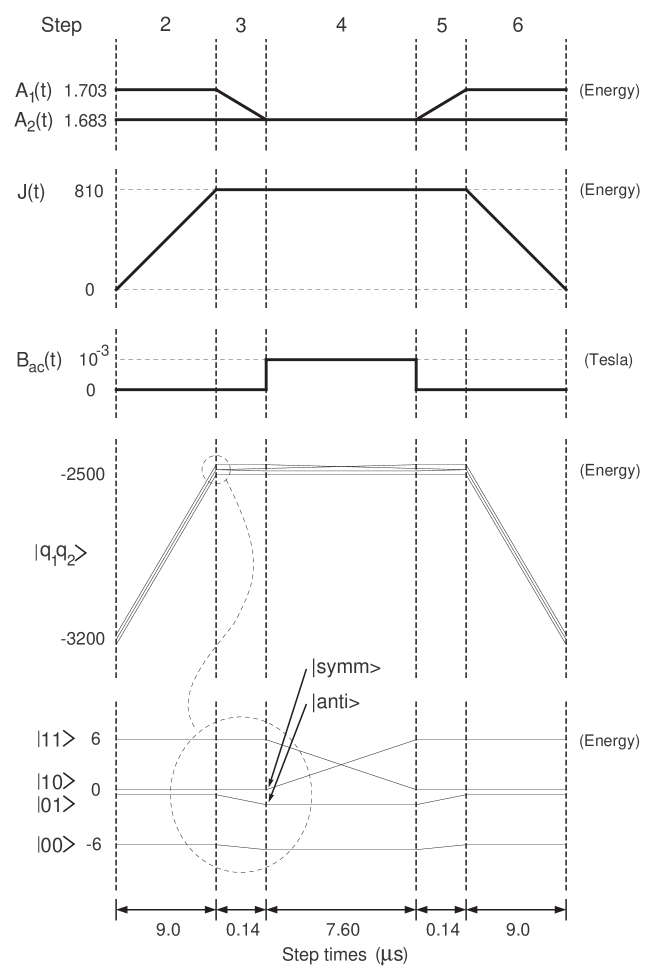
For clarity assume the computer is initially in one of the states , , or and that we wish to perform a CNOT operation with qubit 1 as the control. Step one is to break the degeneracy of the two qubits’ energy levels to allow the control and target qubits to be distinguished. To make qubit 1 the control the value of is increased (qubit 1 will be assumed to be the control qubit for the remainder of the paper).
Step two is to gradually apply a positive potential to the J electrode in order to force greater overlap of the donor electron wave functions and hence greater (indirect) coupling of the underlying nuclear qubits. The rate of this change is limited so as to be adiabatic — qubits initially in energy eigenstates remain in energy eigenstates throughout this step.
Let symm and anti denote the standard symmetric and antisymmetric superpositions of and . Step three is to adiabatically reduce the coupling back to its initial value once more. During this step, anti-level-crossing behavior changes the input states as symm and anti.
Step four is the application of an oscillating field resonant with the symm transition. This oscillating field is maintained until these two states have been interchanged. Steps five to seven are the time reverse of steps one to three. The process is shown schematically in (Fig. 2). Note that steps 1 and 7 (the increasing and decreasing of ) have been omitted as the only limit to their speed is that they be done in a time much greater than eVps where 0.01eV is the orbital excitation energy of the donor electron.
In general the fidelity of the adiabatic steps in the procedure can be increased arbitrarily by making them indefinitely long. In reality, of course, this is not practical and the procedure must be implemented on a time-scale that is short compared to the systems dephasing time. For a given , the degree to which the evolution deviates from perfect adiabaticity can quantified by the measure [24]
| (5) |
It is desired that . Here the states are the set of eigenstates of the Hamiltonian at time . It is possible to reduce without increasing the duration of the step by optimizing the profiles of the time dependent parameters in the Hamiltonian. In the case of the Kane architecture this means optimizing the shape of the evolution of and .


Various profiles for the adiabatic steps in the CNOT procedure have been investigated in [13]. In (Fig. 3), we have plotted three possible profiles for step 2 of the CNOT gate. The function for each profile is shown in (Fig. 4). Profile 1 is a simple linear pulse, profile 2 can be seen to be the best of the three and is described by where is the duration of the pulse and is a factor introduced to ensure that . The third profile
| (6) |
although not quite as efficient as profile 2, is a composite linear-sinusoidal profile that was used in the calculations presented in this paper due to numerical difficulties in solving the Schrödinger equation for profile 2. The advantage of the second two profiles over the linear one is that they flatten out as approaches . At , the system undergoes a level crossing. To maintain adiabatic evolution, needs to change more slowly near this value. Note that the reason it is desirable to make so large is to ensure that there is a large energy difference between symm and anti during step 4 (the application of ). This difference is given by
| (7) |
Without a large energy difference, the oscillating field which is set to resonate with the transition symm will also be very close to resonant with anti causing a large error during the operation of the CNOT gate. While it is desirable to make large, it must be kept comfortably below as near this level crossing the time required to adiabatically increase increases significantly.
Step 3 (the decreasing of ) could be performed without degrading the overall fidelity of the gate in a time of less than a micro-second with a linear pulse profile.
The above steps were simulated using an adaptive Runge-Kutta routine to solve the density matrix form of the Schrödinger equation in the computational basis .
| (8) |
The times used for each stage are as follows
| stage | duration () |
|---|---|
| 2 | 9.0000 |
| 3 | 0.1400 |
| 4 | 7.5989 |
| 5 | 9.0000 |
| 6 | 0.1400 |
Note that the precision of the duration of stage 4 is required as the oscillating field induces the states and symm to swap smoothly back and forth. The duration 7.5989 is the time required for one swap. The other step times were obtained by first setting them to arbitrary values (5) and increasing them until the gate fidelity ceased to increase. The step times were then decreased one by one until the fidelity started to decrease. As such, the above times are the minimum time in which the maximum fidelity can be achieved. This maximum fidelity was found to be for all computation basis states.
4 Intrinsic dephasing and fidelity
In this paper, dephasing is modelled as exponential decay of the off diagonal components of the density matrix. While a large variety of dephasing models exist [25, 26, 27, 28, 29, 30], this approximation is consistent with the first order nature of the spin Hamiltonian. The donor electrons and phosphorous nuclei are assumed to dephase at independent rates. With the inclusion of dephasing terms (Eq. 8) becomes
| (9) | |||||
To understand the effect of each double commutator, it is instructive to consider the following simple mathematical example :
| (14) | |||||
| (19) |
Thus each double commutator in (Eq. 9) exponentially decays it’s associated off diagonal elements with a characteristic time or .
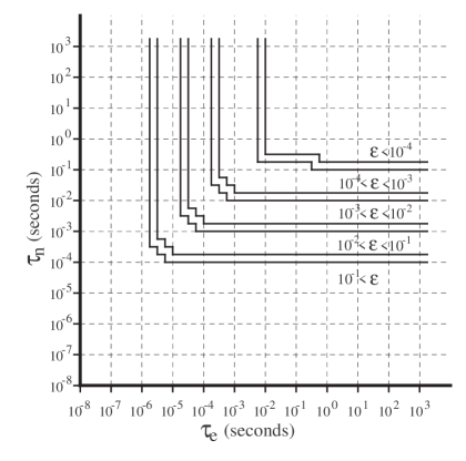
For each initial state , , and (Eq. 9) was solved for a range of values of and using the pulse profiles described in section 3 allowing a contour plot of the gate error versus and to be constructed (Fig. 5). Note that each contour is a double line as each run of the simulation required considerable computational time and the data available does not allow finer delineation of exactly where each contour is. The worst case error of all input states as a function of and is shown in (Fig. 6).
5 Conclusion
At the time of writing, to the authors’ knowledge the only experimental measurement of the 31P in 28Si dephasing times in is [20] in which the donor electron dephasing time T2 was measured at T=1.4K, Bz=0.3T to be 0.5ms. The 28Si sample contained 29Si [19]. Note that a dopant concentration of cm-3 was used implying a donor separation of 50nm. If this T2 is used for and if is assumed to be a couple of orders of magnitude larger as in the case of the relaxation times, then from (Fig. 6) the overall error probability would be just under
Theoretical calculation of and has been performed in [29] for a 2D array of P donors spaced 10nm apart in pure 28Si yielding and s. Such a short would imply an unacceptable error probability of about 10%. However, this same paper also contains similar calculations for natural silicon (4.7% 29Si) with quoted as 200 which leads to an overall error probability just over . The suppression of decoherence in this case arises from line broadening due to the presence of 29Si nuclei. In the case of the Kane quantum computer, similar suppression can be achieved by biasing the A-electrodes such that nearby qubits have different spin-flip energies. Further investigation of this point is required.
Though is a large error probability, numerical simulations by Zalka suggest this may be tolerable [15]. Work is in progress on simulations to determine an acceptable error rate for the Kane architecture.
6 Acknowledgements
The authors thank W. Haig (High Performance Computing System Support Group, Department Of Defence), as well as the Victorian Partnership for Advanced Computing for computational support. This work was funded by the Australian Research Council.
References
- [1] B. Kane, Nature 393, 133(1998)
- [2] P. Benioff, Journal of Statistical Physics 22, 563(1980)
- [3] R. Feynman, International Journal of Theoretical Physics 21, 467(1982)
- [4] P. Shor, Algorithmic Number Theory. First International Symposium, ANTS-I. Procedings, 289(1994)
- [5] L. Vandersypen et. al, Nature 414, 883(2001)
- [6] J. Jones, Progress in Nuclear Magnetic Resonance Spectroscopy 38, 325(2001)
- [7] H-A. Engel, P. Recher and D. Loss, Solid State Communications 119, 229(2001)
- [8] V. Giovannetti, P. Tombesi and D. Vitali, Journal of Modern Optics 21, 467(1982)
- [9] E. Hinds, Physics World, 39(2001)
- [10] D. James, Fortschritte der Physik 48, 823(2000)
- [11] J. Mooij, Microelectronic Engineering 47, 3(1999)
- [12] B. Kane, Forschritte der Physik 48, 1023(2000)
- [13] C. Wellard, PhD Thesis, The University of Melbourne, (2001)
- [14] E. Knill, R. Laflamme and W. Zurek, quant-ph/9702058, (1997)
- [15] C. Zalka, quant-ph/9505011, (1997)
- [16] H.S. Goan and G.J. Milburn, unpublished internal SRC report, (2001)
- [17] G. Feher and E. Gere, Physical Review 114, 1245(1959)
- [18] A. Honig and E. Stupp, Physical Review 117, 69(1960)
- [19] G. Feher and others Physical Review 109, 221(1958)
- [20] J.P. Gordon and K.D. Bowers, Physical Review Letters 10, 368(1958)
- [21] B. Koiler, X. Hu and S. Das Sarma, cond-mat/0106259, (2002)
- [22] A. Larionov, L. Fedichken, A. Kokin and K. Valiev, Nanotechnology 11, 392(2000)
- [23] K. Valiev and A. Kokin, quant-ph/9909008, (1999)
- [24] B.H. Bransden and C.J. Joachain, Introduction to Quantum Mechanics, (1989)
- [25] W.Bauer and W. Nadler, cond-mat/0204325, (2002)
- [26] G. Burkard and D. Loss, Physical Review B 59, 2070(1999)
- [27] K. Kim and H. Kwon, Physical Review A 65, 1(2002)
- [28] D. Mozyrsky, S. Kogan and G. Berman, cond-mat/0112135, (2001)
- [29] R. de Sousa and S. Das Sarma cond-mat/0203101, (2002)
- [30] M. Thorwart, Physical Review A 65, 1(2001)
- [31] D. Gottesman, quant-ph/9903099, (1999)