Demonstration of negative group delays in a simple electronic circuit
Abstract
We present a simple electronic circuit which produces negative group delays for base-band pulses. When a band-limited pulse is applied as the input, a forwarded pulse appears at the output. The negative group delays in lumped systems share the same mechanism with the superluminal light propagation, which is recently demonstrated in an absorption-free, anomalous dispersive medium [Wang et al., Nature 406, 277 (2000)]. In this circuit, the advance time more than twenty percent of the pulse width can easily be achieved. The time constants, which can be in the order of seconds, is slow enough to be observed with the naked eye by looking at the lamps driven by the pulses.
I Introduction
Brillouin and Sommerfeld investigated the propagation of light pulse in a dispersive medium described by the Lorentz model. They pointed out that in the region of anomalous dispersion the group velocity could be larger than , the light velocity in a vacuum, or even be negative Brillouin . The anomalous dispersion occurs near the center of absorption lines. In the case of superluminal group velocities (), the transit time of the light envelope through the medium is shorter than that for a vacuum with the same length. In the case of negative group velocities (), the envelope leaves before it enters into the medium.
Chu and Wong demonstrated experimentally that the light in a Ga:N crystal can be propagated at such extraordinary group velocities Chu . But in these kind of experiments it is inevitable that the shape of the light pulse is largely distorted due to the absorption. The standard definition of the group velocity, , which describes the velocity of the light envelope or peak, tends to lose its physical meaning under the strong distortion of the waveform. A new definition of group velocities, considering the reshape of the spectrum caused by the absorption, was proposed recently Tanaka .
Wang et al. realized anomalous dispersion without absorption using the gain-assisted linear anomalous dispersion, and demonstrated the light propagation at the negative group velocities Wang ; Dogariu . For the light pulse propagation in an absorption-free medium, the normal definition of the group velocity describes precisely the propagating speed of the waveform, or the envelope.
The pulse propagation with superluminal or negative group velocities is very counterintuitive and is liable to cause many misunderstandings. However, it is the direct results of the interference of the wave and is consistent with the relativistic causality.
The anomalous dispersion with no absorption induces phase shifts depending on the frequencies, thereby enhances the front part of the pulse by constructive interference and cancels the rear part by the destructive interference. The pulse shape is conserved if the phase shift is a linear function of the frequency.
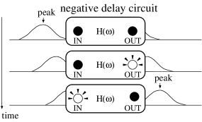
The interference does not occur only in the light propagation, but also in other wave or oscillation dynamics. Signals in electrical circuits also interfere. In lumped systems, we cannot define the group velocities, because there exists no finite length scale. Instead, we can define the group delay. The group delay is the time difference between the input and output signal envelopes. If it is negative, the output pulse precedes the input as shown in Fig. 1. The negative delays are closely connected to the superluminal or negative group velocities in spatially extended systems.
In this paper, we propose a simple electronic circuit which generates negative group delays. While the dispersion relation of dispersive media determines the phase shifts in the light propagation, the transfer function of the circuit determines the phase shifts of the output in reference to the input. Mitchell and Chiao Mitchell demonstrated negative delays in a bandpass filter circuit to which the carrier signal modulated with a pulse is applied. They showed that if the carrier frequency is located outside of the pass band, the envelope of the output pulse precedes the input. In practical implementation, a large inductor is required and it is replaced by a simulated inductor with operational amplifiers. The use of the carrier signal also increases the complication of the circuit.
The circuit that we present here generates negative delays for baseband signals or signals with zero carrier frequency. It is easy to produce negative delays as large as a few seconds, therefore, we can observe it with the naked eye by watching two LEDs (light emitting diodes) each of which is driven by the input and output pulses. It is helpful and illuminating to translate fundamental physical concepts into a simple circuit which replicates the essence of the phenomena Rosner ; Frank .
In the next section we explain the relation between the superluminal or negative group velocity in the light propagation and the negative group delay in lumped circuits. Then, in Sec. III, we present a circuit generating negative group delays and the pulse generator used for the input. In Sec. IV, we propose a method for larger negative delays by cascading the circuits. It is shown that the negative delay time can be increased as without introducing additional distortion of the pulse shape, where is the number of the stages. But for large , the circuit becomes susceptible to the noise.
II Transfer function for negative group delay
In this section we deal with a transfer function in order to study negative group delays. The discussion can be applied to both electric circuits and light propagation in a dispersive medium. A band-limited input signal can be expressed as a product of the carrier and the envelope ; , where represents the complex conjugate term. Our circuit deals with the baseband signal (), but we include the carrier for the purpose of comparison with other cases. The signal is expanded with the Fourier component of the envelope as
| (1) |
where is the bandwidth and is the offset frequency from .
The transfer function is defined for each frequency and the output can be written as
| (2) |
We assume that within the bandwidth (), the amplitude is nearly unity and the phase can be approximated by a linear function, i.e.,
| (3) |
The group delay is defined as
| (4) |
Then the envelope of the output is obtained from Eqs. (2) and (3) as
| (5) |
This means that, aside from the phase factor, the envelope of the output is shifted by the group delay , while maintaining the shape. For , the input precedes the output (normal delay) and for , the output precedes the input (negative delay). We will represent a circuit that satisfies the latter condition in the next section.
In order to translate the above discussion into the light propagation through a dispersive medium with length , we suppose and represent the field of input and that of output of the medium, respectively. When the monochromatic light with frequency is propagated in the medium, the phase of the field is shifted as , where is the wavenumber in the medium. If is linear in the bandwidth, with the help of Eq. (4), we have
| (6) |
where is the group velocity . The envelope of the light is delayed by .
If the difference between the propagation time of the envelopes in the dispersive medium and that in a vacuum with the same length is negative, i.e.,
| (7) |
then the light propagation in the medium is called superluminal. There are two cases which satisfy this condition; and . In the former case, the output envelope precedes the output for the vacuum case but does not precede the input. In the latter case, the output precedes the input, or the whole system provides the negative group delay .
III Circuits and experiment
III.1 Negative delay circuit for baseband signals
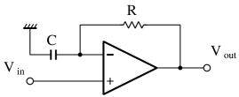
In Fig. 2, we show a negative delay circuit for baseband () signals. This is basically a non-inverting (imperfect) differentiator. Its transfer function is easily obtained as
| (8) |
where .
We note that the corresponding action in the time domain is . The advancement of a pulse can be understood qualitatively. For the rising edge, which has a positive slope, the two terms interfere constructively, while for the falling edge with a negative slope, they interfere destructively. Thus the pulse is forwarded.
In the low-frequency region ( ), is approximated as
| (9) | ||||
| (10) |
which mean that the amplitude is nearly constant and the phase increases linearly with frequency. Then the group delay becomes negative:
| (11) |
As seen in Fig. 3, the amplitude and the phase of the transfer function are not linear except in owing to the higher order terms in Eqs. (9) and (10). These terms induce waveform distortion of the output. In order to keep the distortion as small as possible, the spectrum of the input signal must be restricted within the frequency region . For this purpose low-pass filters are needed.


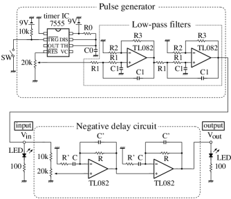
III.2 Low-pass filter
In order to prepare a band-limited, base-band pulse we introduce low-pass filters. The initial source is a rectangular pulse from a timer IC (integrated circuit). The rectangular pulse has high-frequency components, and the negative delay circuit does not work correctly. We must eliminate the high-frequency components with low-pass filters. We introduce two 2nd-order low-pass filters shown in Fig. 4. Each transfer function is
| (12) |
where and . By changing , we can tailor the characteristic of the filter. In our experiment we choose the value , which corresponds to a Bessel filter Tietze . The Bessel filter is designed so that the overshoot for rectangular waves is small. The cut-off frequency is defined by .
III.3 Experiment
We show the overall circuit diagram for the negative delay experiment in Fig. 4 and the parameters in Table 1.
The pulse generator in the upper section of Fig. 4 is subdivided into the generator of single-shot rectangular wave and the low-pass filters. In the first part, when triggered by the switch, the timer IC generates a single pulse, whose width is determined by the time constant . The rectangular pulse is shaped by the two-stage low-pass filters. The total order of low-pass filter is . We set the cut-off frequency of the low-pass filter as , so that and can be considered to be constant and linear, respectively, below the cut-off frequency (see Fig. 3). Finally, the band-limited single pulse is sent out for the input of the negative delay circuit in the lower section of Fig. 4.
Two delay circuits shown in Fig. 2 are cascaded for larger advance time. The input and output terminals are monitored by LEDs. Their turn-on voltage is about . The variable resistor at the input is adjusted so that the input and the output have the same height.
The experimental result is shown in Fig. 5. The input and output waveforms are recorded with a oscilloscope. The origin of the time () is the moment when the switch in Fig. 4 is turned on. We see that the output precedes the input considerably (more than 20% of the pulse width). The slight distortion of the output waveform is caused by the non-ideal frequency dependence of and , as mentioned in Sec. III.1.
The expected negative delay derived from Eq. (11) is ; we have connected two circuits (each time constant ) in series for larger effect. This quantitatively agrees with the experimental result, where the time difference between the output and the input peaks is about . The time scale is chosen so that one can directly observe the negative delay with two LEDs connected at the input and the output terminals. We could also use two voltmeters (or circuit testers) to monitor the waveforms. We could dispense with an oscilloscope.
The actual negative delay circuit in Fig. 4 differs from that shown in Fig. 2. The resistor and the capacitor are supplemented for the suppression of high-frequency noises. As shown in Fig. 3, the gain at is large. Although the high-frequency components of the input signal are suppressed by the low-pass filters, the internal and external noises with high frequency are unavoidable. With and , the high-frequency gain is limited. The parameters are chosen as so that the phase for is not affected.

IV Realization of larger negative delay

The obtained negative delay in the above experiment is about 20% of the pulse width. This is larger than the values obtained in other superluminal-velocity or negative-delay experiments. We consider the way to make even larger negative delays. We assume noise-free environment for a simplicity.
Cascading the negative delay circuits, the time advance can be increased. One might simply expect that, by increasing the number of stages , the total time advance can be increased linearly with . But, unfortunately, this is not the case. It is obvious from Eqs. (9) and (10) that the distortion of the waveform of the output is also increased. When circuits are connected in cascade, the total transfer function can be written as . Correspondingly, the amplitude and the phase are given as
| (13) | ||||
| (14) |
In order to keep the wave distortion below a certain level, we have to limit the excess gain within the bandwidth by some value ;
| (15) |
Then the advance time per circuit should satisfy
| (16) |
where is the pulse width. It is determined by the cut-off frequency of the low-pass filter.
If we want to increase the time advance in conserving the pulse width and the distortion of the signal, we must reduce the time advance per circuit by the factor . Therefore, the total time advance scales as
| (17) |
which is a slowly increasing function of .
In addition, there is another factor to be considered. A causal transfer function cannot generate negative delays unconditionally. It is impossible to advance the signal beyond the time when the switch is turned on in the rectangular pulse generator in Fig. 4. The reason of the advancement is that the slow rising part of the pulse, which has been suppressed by the low-pass filter, is reemphasized by the negative delay circuit. The slowness of rising part of the pulse is determined by the order of the low-pass filter. Figure 6 represents responses of various order Bessel filters with the same cut-off to a rectangular wave with a unit height and a pulse width . The pulse shapes, especially the widths of the pulses, are similar to each other owing to the same cut-off frequency, but the higher the order of filter the more the rising part is delayed. Hence we need a high order filter to attain large time advance. In other words, the pulse must be delayed appropriately in advance in order to get a large negative delay.
Moreover the short-time behavior of the total circuit including the low-pass filters and the negative delay circuits is determined by the composite transfer function at high frequency (). The order of the low-pass filter should not be smaller than the number of the stages of the negative delay circuits. Otherwise the total transfer function would diverge at and the derivative of the rectangular pulse would appear at the output.
Figure 7 represents a result of simulation for the response of ten negative delay circuits with the input of a tenth order Bessel filter. The used parameters are and . The total time advance is estimated from Eq. (17). This estimation is consistent with the result of the simulation. The advance time is comparable to the pulse width. It is so large that the input starts to rise when the output begins to fall.

V Discussion and conclusion
Let us consider a positive delay circuit. A circuit called all-pass filter has the transfer function Tietze :
The all-pass filter can be build with an operational amplifier, three resistors, and a capacitor. It is very convenient for generating positive delays for base-band signals because the amplitude and phase of the transfer functions are given as , and , respectively. The flat amplitude response allows us to cascade the circuits without introducing pulse distortion and results in the delay . Unfortunately the negative version () of all-pass filter
will not work because it is not causal. The pole of , , is located in the right half plain. If one makes this circuit, it will be unstable owing to the time response function . This example tells us about the asymmetry between the negative delay and the positive delay. The former is much more difficult to achieve than the latter.
The group velocity has no direct connection with the relativistic causality, therefore, it can exceed the speed of light in a vacuum. But the front velocity (or the wavefront velocity) is constrained by the causality and is equal to , namely, . In lumped systems (), the wavefront delay must vanish. Actually all of the pulses in our system have their wavefronts at , the moment when the original rectangular pulse rises or the switch is turned on.
To conclude, we demonstrated the negative group delay in a simple electronic circuit. A considerably large negative delay () could easily be achieved. It is slow enough to be observed with the LEDs or voltmeters with the naked eye. The negative delay amounts to 20% of the pulse width. In the light experiment Wang , is and is only a few percents of the pulse width, .
Including the pulse generator for the input of the negative delay circuit, the apparatus consists of common parts available in any laboratories. It is so simple that a beginner can build it in an hour. The setup can be operated stand-alone and no expensive instruments such as oscilloscopes and function generators are required. It is useful for understanding the physics of superluminal propagation as well as the negative group delays.
Acknowledgements.
This research was supported by the Ministry of Education, Culture, Sports, Science and Technology in Japan under a Grant-in-Aid for Scientific Research No. 11216203 and No. 11650043.References
- (1) L. Brillouin, Wave Propagation and Group Velocity (Academic Press, New York, 1960) pp. 113 – 137.
- (2) S. Chu and S. Wong, “Linear Pulse Propagation in an Absorbing Medium,” Phys. Rev. Lett. 48, 738 – 741 (1982).
- (3) M. Tanaka, M. Fujiwara, and H. Ikegami, “Propagation of a Gaussian wave packet in an absorbing medium” Phys. Rev. A 34, 4851 – 4858 (1986).
- (4) L. J. Wang, A. Kuzmich, and A. Dogariu, “Gain-assisted superluminal light propagation,” Nature 406, 277 – 279 (2000).
- (5) A. Dogariu, A. Kuzmich, and L. J. Wang, “Transparent anomalous dispersion and superluminal light-pulse propagation at a negative group velocity,” Phys. Rev. A 63, 053806-1 – 053806-11 (2001).
- (6) M. W. Mitchell and R. Y. Chiao, “Causality and Negative Group Delays in a Simple Bandpass Amplifier,” Am. J. Phys. 66 (1), 14–19 (1998).
- (7) J. L. Rosner, “Tabletop time-reversal violation,” Am. J. Phys. 64 (8), 982–985 (1996).
- (8) W. Frank and P. Brentano, “Classical analogy to quantum mechanical level repulsion,” Am. J. Phys. 62 (8), 706–709 (1994).
- (9) U.Tietze and Ch. Schenk, Electronic Circuit (Springer-Verlag, Berlin, 1991) pp. 350–408.