Room temperature stable single-photon source
Abstract
We report on the realization of a stable solid state room temperature source for single photons. It is based on the fluorescence of a single nitrogen-vacancy (NV) color center in a diamond nanocrystal. Antibunching has been observed in the fluorescence light under both continuous and pulsed excitation. Our source delivers s-1 single-photon pulses at an excitation repetition rate of MHz. The number of two-photon pulses is reduced by a factor of five compared to strongly attenuated coherent sources.
pacs:
42.50.Dv, 03.67.-a, 78.67.-nI Introduction
The security of quantum cryptography is based on the fact that quantum mechanics does not allow one to duplicate an unknown state of a single quantum system (for a review see TRG ). This property is referred to as the no-cloning theorem. After the pioneering experiment of the group of Bennett and Brassard BBBSS , several quantum key distribution set-ups using attenuated laser pulses have been demonstrated (see for example refs TRG ; BHLMNP ). In these implementations, single photons are approximated by strongly attenuated coherent pulses so that the average number of photons per pulse is . In this case, the probability of having two photons in a pulse is approximately LoiPoisson . Two-photon pulses are a potential information leakage source L . Indeed, an eavesdropper could tap on the communication between the sender (Alice) and the receiver (Bob), by keeping one of the two photons and sending the other one to Bob. The eavesdropper can then measure the state of the photon once Alice and Bob have revealed their measurement basis. With attenuated coherent pulses, the only way to reduce the probability of having two photons in a pulse is to lower and thereby decreasing the transmission rate. Our aim is to realize an efficient single-photon source that would have a vanishing two photon probability for a non vanishing transmission rate.
Single photons on demand can be produced by pulsed excitation of a single dipole MGM ; pra . The principle is that a single emitting dipole has to undergo a full excitation-emission-reexcitation cycle before emitting a second photon. For a sufficiently short and intense excitation pulse, a single dipole emits one and only one photon pra .
Several solid state sources, like single organic molecules BMOT ; BLTO ; KJRT ; wild ; ML ; TCGR , self-assembled semiconductor quantum dots YY ; I2 ; ZBJPJTGPSB , or semiconductor nanocrystals I1 have been presented lately as potential candidates. However, the ideal candidate should be photostable, work at room temperature and be easy to manipulate. Single nitrogen-vacancy (NV) color centers in bulk diamond GDTFWB have recently been shown to exhibit strong antibunching at room temperature ol ; capri ; KMZW . They are intrinsically photostable and are believed to have a unity quantum efficiency efficiency . The high refractive index of diamond leads however to small a collection efficiency owing to total internal reflection and spherical aberrations. Also, the signal to background ratio is limited by the light emitted from the surrounding diamond crystal. One can also point out that bulk diamond cannot be manufactured in any desirable shape, and thus is very difficult to handle and insert, for example, into a microcavity.
In this paper, we show that the use of single NV color center in diamond nanocrystals (typical size nm) is a very convenient solution to these problems. The subwavelength size of the nanocrystals renders refraction irrelevant. One can simply think of the nanocrystal as a point source emitting light in air. Furthermore, the small volume of diamond excited by the pump light reduces the emitted background light. Also, diamond nanocrystals can be easily handled in order to be inserted in a cavity or to be deposited on a fiber tip KHSPV . In addition NV centers in diamond nanocrystals preserve all the important features of NV centers in bulk diamond. In particular, we have checked that the fluorescence spectrum of NV centers in nanocrystals at room temperature is the same as in bulk. By investigating the autocorrelation function under continuous wave (CW) and pulsed excitation, we demonstrate the possibility to use NV centers in diamond nanocrystals as a room temperature stable single-photon source.
II Experimental set-up
The color center used in our experiments is the NV defect center in synthetic Ib diamond, with a zero phonon line at a wavelength of nm GDTFWB . The defect consists in a substitutional nitrogen and a vacancy in an adjacent site. A simplified level structure is a four-level scheme with fast non radiative decays within the two upper states and within the two lower states. This amounts to an incoherent two-level system. The lifetime of the excited state in the bulk is ns CTJ .
NV centers are artificially created in synthetic MDA diamond powder from de Beers. Nitrogen is naturally present in diamond. Vacancies are created by irradiation with MeV electrons at a dose of cm2. Subsequent annealing in vacuum at C during hours leads to the formation of NV centers GDTFWB . The nanocrystals are dispersed by sonification in a solution of polymer (Polyvinylpyrrolidone at 1 weight in propanol). This allows the disaggregation of the particles and their stabilization in a colloidal state. Centrifugation at 11000 rpm for 30 min allows us to select nanocrystal sizes of nm (measured by dynamical light scattering). The average number of NV centers in a nanocrystal has been evaluated to (see below). Nanocrystals containing a single NV center should therefore have a size around nm, which lies in the lower wing of the size distribution. The nanocrystal solution is then spin coated at 3000 rpm on thin fused silica substrates. Evaporation of the solvent leaves a 30 nm thick film of polymer with the nanocrystals well dispersed on the surface. Their density was estimated to be around m-2. In most experiments we look at the centers from the other side of the plate, which is in contact with the oil of an immersion microscope lens (Nachet 004279, N.A. = 1.3).
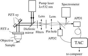
The experimental setup (fig. 1), based on a confocal microscope, has been described in detail elsewhere ol ; capri . The pump laser (CW or pulsed) is focused with an immersion oil, high numerical aperture objective (), onto a diffraction limited spot ( nm FWHM). The fluorescence light is collected by the same objective and after proper frequency and spatial filtering, it can either be send on a spectrometer, or to a Hanbury-Brown and Twiss set-up using two avalanche photodiodes (APD) from EGG. Appropriate data processing allows us to obtain the histogram of the time separations between successive photons. A slow (8s response time) x-y-z computerized servo-loop is used to compensate for any drifts. Bandpass filters allow detection from to nm. This spectral window matches the broad emission spectrum of a NV center GDTFWB .
III Continuous wave excitation
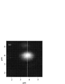

At first, we investigate the fluorescence of single NV centers in nanocrystals under CW excitation with a frequency doubled YAG laser ( nm). Fig. 2(a) displays a 2D scan of a single NV center. From the line scan in fig.2(b) we deduce a spatial resolution of nm and a signal (S) to background (B) ratio of . The corresponding value in the bulk is (see fig. 3).
Fig. 3 shows the saturation behavior of the fluorescence rate of NV centers in bulk and in nanocrystals with respect to pump power. The slightly decreasing rate at high pump power is due to a trapping metastable state capri . The saturating count rate in a diamond nanocrystal ( s-1) is slightly lower than that in bulk diamond ( s-1), but one has to take into account the longer lifetime of a NV center in a nanocrystal (see at the end of this section). The number of photons detected in a lifetime is in the nanocrystal (lifetime ns) and in bulk diamond (lifetime ns). This means that the geometrical collection efficiency for nanocrystals is increased by .
It can also be seen in fig. 3 that the contribution of background next to the nanocrystal is greatly reduced. The background coming from the diamond nanocrystal itself is reduced mainly because the excited volume of diamond is smaller.
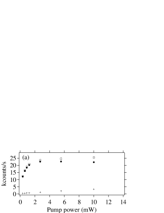

The evaluated overall detection efficiency is given by , where for the bulk or for a nanocrystal, respectively. The geometrical collection efficiencies for a dipole oriented orthogonally to the optical axis are and (calculated). The optical transmission from the sample to the detectors is (measured), and the detector quantum efficiency is (taken from the data sheet). In addition the NV center presents a metastable state in which the excitation can be shelved GDTFWB ; capri ; KMZW . This leads to a reduction of the count rate by a factor equal to the saturated population of the excited state. This value has been inferred by fitting a saturation curve (cf fig. 3) and a set of autocorrelation functions (like fig. 4) obtained for different pump powers capri . This fit involves many parameters and gives only approximative results. For a nanocrystal, the saturated count rate should then be s-1, which is times more than what we actually detected ( s-1). This discrepancy exists also in bulk and its origin is still under investigation efficiency .
We have also studied the autocorrelation function of the fluorescence of single NV centers in diamond nanocrystals. The raw coincidences (right axis) and autocorrelation function (left axis) are represented in fig. 4.
For evaluating the intensity correlation function of the NV center, the raw correlation data is normalized and corrected in the following way. The raw coincidence rate counted during a time within a time bin of width is first normalized to that of a Poissonian source according to the formula
| (1) |
where are the count rates on each detector. The normalized coincidence rate is then corrected for the background light , and we obtain
| (2) |
where is related to the signal to background ratio, which is measured independently in each experimental run by measuring the count rate next to the nanocrystal (see fig. 2(b)). This takes into account only the background coming from the fused silica and the polymer, and not the parasitic light emitted by the diamond nanocrystal itself. Note that we have checked experimentally that the background light has a Poissonian statistics.
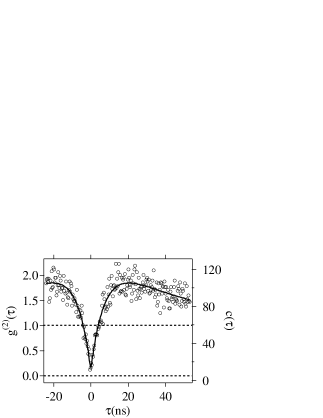
It can be seen in fig. 4 that , where the slight difference with zero is attributed to remaining background light emitted by the nanocrystal and electronic jitter of the avalanche photodiodes ( ps). This almost vanishing value of is the signature of the presence of a single emitter in the observed nanocrystal. In the case of the presence of centers within a nanocrystal, the value of the zero-time antibunching is . This is actually how we estimate the number of NV centers in a nanocrystal.
We have obtained a normalized coincidence rate at the fluorescence rate maximum (input power of mW), where the best value in bulk diamond was capri ; KMZW . As we shall see in the next section, this uncorrected normalized coincidence rate is the relevant parameter for characterizing a single photon source.
It should also be mentioned that reaches values greater than unity for ns. This bunching effect for longer time scale is due to the presence of the trapping metastable state in which the system can be shelved KJRT ; DFTJKNW ; capri ; BFTO . This effect can also be seen as blinking on a time scale of ns. The time distribution of photons can ve viewed as bursts of photons of about ns duration. In each burst the delay between successive photons is always larger than ns (antibunching).
In a low pump regime, the central dip in the antibunching traces can be fitted by an exponential function with the argument , where , with being the NV center spontaneous decay rate and the pumping rate capri . Such fits have been performed for different pumping powers. The inverse lifetime of an NV center in a nanocrystal can then be inferred by extrapolating the value of the time constant for vanishing pump power (fig. 5). We deduce a lifetime for NV centers in bulk diamond of ns CTJ whereas the lifetime is found to be ns in diamond nanocrystals qph . This value has been obtained by observing different nanocrystals. A possible explanation for this lifetime increase is that the refractive index experienced by the emitted light is different in bulk diamond and nanocrystals. When working out the spontaneous emission rate from the Fermi’s golden rule, it turns out that this rate is proportional to the refractive index of the material in which the dipole is radiating.

In our case, the NV center in bulk diamond emits within a medium of index , whereas the center in a sub-wavelength nanocrystals emits as if it were in air for one half of the space, and in fused silica (refractive index ) for the other half. The expected lifetime is then ns in good agreement with the experimental values. A full description of lifetime changes due to refractive index is a controversial subject mainly because of local field correction issues gl ; cc ; cb . However, our results tend to show that the local field experienced by the NV center in bulk and in nanocrystals is the same qph . As mentioned earlier no substantial difference in the emission spectrum of NV centers in nanocrystals and in bulk has been found. This is a good indication that the observed lifetime change is mainly due to the modification of the refractive index of the medium in which the NV center is radiating.
IV Pulsed excitation
The pulsed excitation consists of a home build source along the lines of reference pct . The output of a mW continuous wave Nd:YAG laser ( nm) is coupled into a fast ( GHz) integrated LiNbO3 modulator (Alenia) which slices up pulses of ns duration at a repetition rate of MHz. The pulses are then amplified to W mean power by an Ytterbium fiber amplifier (Keopsys) and frequency doubled using a PPKTP crystal. In this way we obtain pulses at ns of energy nJ.
We investigate the intensity autocorrelation function of the fluorescence light of a single NV center in a nanocrystal under pulsed excitation. For a Poissonian source the probability of having a coincidence between two photons in the same pulse, or two photons coming from different pulses, is equal. Therefore the autocorrelation function for a pulsed Poissonian source exhibits peaks of same height separated by the repetition period (fig. 6).
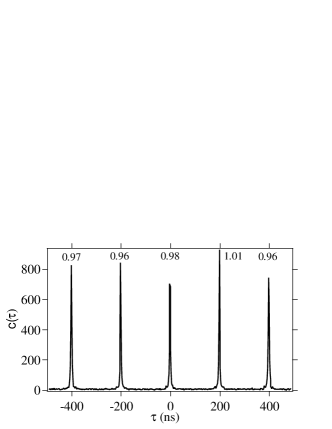
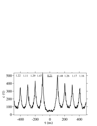
In fig. 7 is shown the intensity autocorrelation function of a single NV center under pulsed excitation. The excitation pulse duration is ns and the repetition period is ns. It can be seen that the peak around is missing, which implies that the probability of having two photons in one pulse is strongly reduced. This gives rise to a highly sub-Poissonian light source. In order to compare our single photon source to a pulsed Poissonian light source, one has to normalize the area of peak number to the area of a peak corresponding to a pulsed Poissonian distribution with the same count rate, with being the total acquisition time. Analogously to eq.(1), the normalized area of each peak is given by
| (3) |
The determination of the area is performed in the following way. The peaks are fitted by exponential decays with the same lifetime. We checked that the lifetime found from the fit is the same than that deduced from the CW excitation. This fitting procedure allows an accurate evaluation of the area of peak , in spite of the significant overlap between peaks. The normalized peak areas are given by the numbers displayed above each peak in fig. 7. For a Poissonian pulsed light source for all (see fig. 6). For our single dipole in the most favorable case, in which the NV center is saturated but the zero time peak is as low as possible, we obtained . Note that this value is slightly larger than . This is attributed to the finite duration ( ns) of the exciting pulses pra .
Let us recall that the probability of having two photons in a pulse is given by (assuming )
| (4) |
where is the probability of having a single photon. Note that for Poissonian light , and eq.(4) with gives the photon probability distribution of an attenuated coherent pulse. The zero time normalized coincidence rate means that the rate of two photon pulses is nearly five times lower than for Poissonian light. Since our source has a single photon rate of s-1 at an excitation repetition rate of MHz, its rate of two-photon pulses is only of s-1.
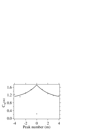
It can also be observed that the peaks grow above unity. Just as in fig. 4, this bunching effect for non zero time scale comes from the existence of a metastable state KJRT ; GDTFWB ; capri ; KMZW ; BFTO . In fig. 8 we have plotted the normalized area of the first peaks. The long time decay behavior can be described by a simple model assuming that the NV center gets randomly trapped in the metastable state. This results in random blinking of the NV center. The normalized area of peak is then given by YY
| (5) |
where is the mean time during which the excitation is trapped in the metastable state and the emission is inhibited and is the mean time during which the center is emitting. Fitting the normalized peak area (cf fig. 8) with eq.(5) allows us to extract the values ns, ns. The saturated count rate should then be s-1, while we detect only s-1. This is the same discrepancy that what was observed for CW excitation efficiency . Note that the factor accounts for the shelving state and plays the same role as for CW excitation. Their different values are attributed to the fact that the shelving and deshelving rates depend on the excitation power capri and are therefore different in CW and in pulsed regime.
V Conclusion
In this paper we have demonstrated the possibility of using single NV centers in diamond nanocrystals as a room temperature solid state source for single photons. They present the advantages of being photostable and easy to manipulate. Furthermore the fabrication of the samples is easy and inexpensive. The single photon rate summed over both photodiodes is s-1 for an excitation repetition rate of MHz. Our source exhibits a strong sub-Poissonian distribution. The two photon pulse rate is reduced by a factor of five compared to a Poissonian source and is equal to s-1. Improvements in the collection efficiency should be obtained by depositing the nanocrystals on a mirror or inserting them into a microcavity. Even though the repetition rate is low compared to what can be obtained with attenuated pulses using laser diodes, the reduction by a factor of 5 of the two photon pulses will allow a secure transmission over larger distances L .
VI Acknowledgements
We thank F. Treussard and R. Pansu for lending us crucial electronic equipment, P. Georges for constructive discussions on the pulsed laser system, E. Bréelle from the “Groupe de Physique des Solides” at Paris 6 for the sample irradiation, and A. Machu for sample annealing. This work is supported by the European IST/FET program “Quantum Information Processing and Telecommunication”, project number 1999-10243 “S4P”. SK is supported by a Marie Curie fellowship from the European Union.
References
- (1) N. Gisin, G. Ribordy, W. Tittel, and H. Zbinden, to appear in Rev. Mod. Phys, and references therein. See also quant-ph/0101098.
- (2) C.H. Bennett, F. Bessette, G. Brassard, L. Salvail, and J. Smolin, Journal of Cryptology 5; 3-28 (1992)
- (3) W. T. Buttler, R. J. Hughes, P. G. Kwiat, S. K. Lamoureaux, G. L. Morgan, J. E. Nordholt, C. G. Peterson, and C. M. Simmons, Phys. Rev. Lett. 81 3283 (1998).
- (4) This approximation is valid if the mean photon number per pulse is smaller than unity.
- (5) N. Lütkenhaus, Phys. Rev. A 59, 3301 (1999); G. Brassard, N. Lütkenhaus, T. Mor, and B. C. Sanders, Phys. Rev. Lett. 85, 1330 (2000).
- (6) F. de Martini, G. di Guiseppe, and M. Marrocco, Phys . Rev. Lett. 76, 900 (1996).
- (7) R. Brouri, A. Beveratos, J.-Ph. Poizat, and P. Grangier, Phys. Rev. A 62, 063817 (2000)
- (8) Th. Basché, W. E. Moerner, M. Orrit, and H. Talon, Phys. Rev. Lett. 69, 1516 (1992)
- (9) C. Brunel, B. Lounis, Ph. Tamarat, and M. Orrit, Phys. Rev. Lett. 83, 2722 (1999)
- (10) S. C. Kitson, P. Jonsson, J. G. Rarity, and P. R. Tapster, Phys. Rev. A 58, 620 (1998).
- (11) L. Fleury, J.M. Segura, G. Zumofen, B. Hecht, and U.P. Wild, Phys. Rev. Lett. 84, 1148 (2000).
- (12) B. Lounis and W.E. Moerner, Nature 407, 491 (2000).
- (13) F. Treussart, A. Clouqueur, C. Grossman, and J.-F. Roch, Opt. Lett. 26, 1504 (2001).
- (14) C. Santori, M. Pelton, G. Solomon, Y. Dale, and Y. Yamamoto, Phys. Rev. Lett. 86 1502 (2001).
- (15) P. Michler, A. Kiraz, C. Becher, W. V. Schoenfeld, P. M. Petroff, L. Zhang, E. Hu, and A. Imamoğlu, Science 290, 2282 (2000)
- (16) V. Zwiller, H. Blom, P. Jonsson, N. Panev, S. Jeppesen T. Tsegaye, E. Goobar, M.-E. Pistol, L. Samuelson, and G. Björk, Appl. Phys. Lett. 78, 2476 (2001)
- (17) P. Michler, A. Imamoğlu, M.D. Mason, P.J. Carson, G.F. Strouse, and S.K. Buratto, Nature 406, 968 (2000).
- (18) A. Gruber, A. Dräbenstedt, C. Tietz, L. Fleury, J. Wrachtrup, and C. von Borczyskowki, Science 276, 2012 (1997).
- (19) R. Brouri, A. Beveratos, J.-Ph. Poizat, and P. Grangier, Opt. Lett. 25, 1294 (2000)
- (20) A. Beveratos, R. Brouri, J.-Ph. Poizat, and Ph. Grangier, QCMC 3 Proceedings (Kluver Academic/Plenum Publisher) (2000) (see also arXiv:quant-ph/0010044).
- (21) C. Kurtsiefer, S. Mayer, P. Zarda, and H. Weinfurter, Phys. Rev. Lett. 85, 290 (2000)
- (22) Unity quantum efficiency implies that the only way for the excited dipole to loose its excitation is by emitting a photon. In E. Pereira, Datareview 7.2, Properties and growth of diamond, Ed G. Davies, (INSPEC, The Institution of Electrical Engineers, London, 1994), the author gives a quantum efficiency deduced from the experimental data of CTJ . This deduction is made by saying that the temperature independence of the luminescence lifetime means that non-radiative decays are absent and therefore that the quantum efficiency is unity.
- (23) Diamond nanocrystals have been used as nanoscopic light source for Scanning Near-field Optical Microscopy (SNOM) in S. Kühn, C. Hettich, C. Schmitt, J.-Ph. Poizat, and V. Sandoghdar, J. Microscopy 202,2 (2001).
- (24) A. T. Collins, M. F. Thomaz, and M. I. B. Jorge, J. Phys. C: Solid State Phys. 16, 2177 (1983).
- (25) A. Dräbenstedt, L. Fleury, C Tietz, F. Jelezko, S. Kilin, A. Nizovtev, and J. Wrachtrup, Phys. Rev. B 60, 11503 (1999).
- (26) J. Bernard, L. Fleury, H. Talon, and M. Orrit, J. Chem. Phys. 98, 850 (1993).
- (27) A. Beveratos, R. Brouri, T. Gacoin, J-Ph. Poizat, and Ph. Grangier, to appear in Phys. Rev. A. See also quant-ph/0104028.
- (28) R. J. Glauber and M. Lewenstein, Phys. Rev. A 43, 467 (1991).
- (29) G. L. J. A. Rikken and Y. A. R. R. Kessener, Phys. Rev. Lett. 74, 880 (1995); F. J. P Schuurmans, D. T. N. de Lang, G. H. Wegdam, R. Sprik, and Ad. Lagendijk Phys. Rev. Lett. 80, 5077 (1998) and references therein.
- (30) M. E. Crenshaw and C. M. Bowden, Phys. Rev. Lett. 85, 1851 (2000).
- (31) S.V. Popov, S.V. Chernikov, and J.R. Taylor, Opt. Comm. 174, 231-234 (2000).