Microoptical Realization of Arrays of Selectively Addressable Dipole Traps:
A Scalable Configuration for Quantum Computation with Atomic Qubits
Abstract
We experimentally demonstrate novel structures for the realisation of registers of atomic qubits: We trap neutral atoms in one and two-dimensional arrays of far-detuned dipole traps obtained by focusing a red-detuned laser beam with a microfabricated array of microlenses. We are able to selectively address individual trap sites due to their large lateral separation of 125 m. We initialize and read out different internal states for the individual sites. We also create two interleaved sets of trap arrays with adjustable separation, as required for many proposed implementations of quantum gate operations.
pacs:
03.67.-a, 32.80.Pj, 42.50.-pThe dramatic progress in micro- and nanofabrication of the hardware for information technology will lead to the encoding of logical information on a single particle basis in the near future. Therefore, the quantum behavior of the physical carriers of information has to be considered. Moreover, quantum effects may provide qualitatively new modes for information processing driving research in the field of quantum information processing [1].
Among the broad range of currently investigated approaches, important progress has been obtained with atom physical schemes. Entanglement and quantum gate operations have been achieved with trapped ions [2] or photons in cavity QED experiments [3]. Several schemes for quantum gates based on the direct interaction of neutral atoms have been proposed theoretically [4, 5, 6, 7]. Still, there is an intensive search for appropriate systems allowing the experimental realisation of these schemes.
Several requirements have to be fulfilled for the sucessful implementation of quantum computation [8], such as the scalability of the physical system, the capability to initialize and read out qubits, long decoherence times, and the existence of a universal set of quantum gates. These requirements are potentially met by setups which are based on miniaturized structures for trapping, guiding, and manipulating neutral atoms as it is investigated in the newly developing field of integrated atom optics or ATOMICS [9]. This approach draws its strength from the combination of the well developed techniques for the manipulation of atomic quantum states with the state-of-the-art manufacturing basis of micro- and nanofabrication. A number of groups use microfabricated charged and current carrying structures for this purpose [10, 11, 12, 13, 14, 15, 16, 17].
As an alternative approach, we have proposed the application of microfabricated optical elements (microoptical elements) and have developed a number of configurations for atom optics, atom interferometry, and quantum information processing [18, 19]. We consider this approach to be extremely powerful since most of the techniques for manipulating atomic qubits are based on the interaction with light and since optical trapping potentials can be made state selective in a simple fashion as required for many quantum gate proposals [4, 5, 6].
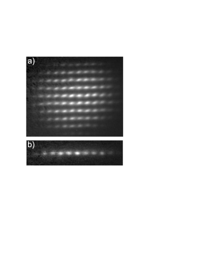
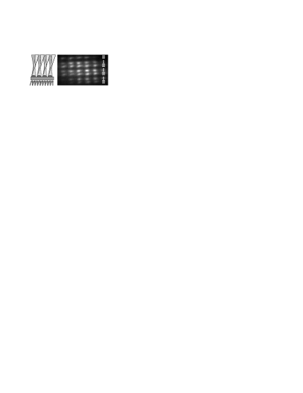
In this paper we present the first experimental implementation of microfabricated optical systems for quantum computing purposes with atoms: Figure 1 shows rubidium atoms trapped in one and two-dimensional arrays of dipole traps created by a microoptical system. More than 80 traps hold atoms in Fig. 1 (a). Each trap can act as a memory site for quantum information encoded in the two hyperfine groundstates of the atoms. Thus, the arrays can serve as registers of atomic qubits.
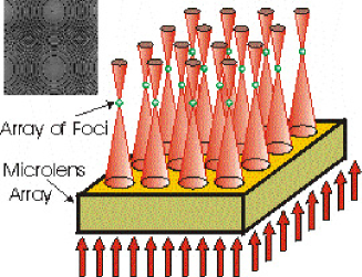
We obtain the trap arrays by employing a two-dimensional array of spherical, diffractive microlenses with a focal length of 625 m and a lens diameter and separation of 125 m (inset in Fig. 2). The microlens array is made of fused silica and contains 50x50 diffractive lenslets. The trapping light is derived from a 500 mW amplified diode laser system and is sent through a rubidium gas cell heated to a temperature of 110 serving as a narrowband absorption filter. This reduces the strong background of amplified spontaneous emission by at least two orders of magnitude otherwise preventing the operation of a dipole trap due to scattering of resonant photons. The light is then sent through an acoustooptical switching device and through a polarizer, which ensures a high degree of linear polarisation. The remaining light (typical power P = 100 - 200 mW, typical detuning = 0.2 to 2 nm below the transition at 780 nm (’red-detuning’)) is focused by the microlens array. In order to have full optical access for atom preparation and detection, we image the focal plane of the microlens array onto a magnetooptical trap (MOT) with the help of two achromats (magnification = 1 and no significant reduction of numerical aperture). Thus, we obtain an array of foci with a separation of 125 m and a spot size of (m (-radius of intensity). For a red-detuned laser beam this results in an array of dipole traps, each analogous to a trap obtained by a single focused laser beam [20, 21] (see also [22]). The optical transfer of the trapping light has the additional advantage that we can place the microoptical system outside the vacuum chamber and thus can switch between a variety of microoptical elements easily. On the other hand, trapping of atoms directly in the first focal plane close to the surface is possible as well.
We load the array of dipole traps and detect the trapped atoms similar to [23]: We start with a MOT of to atoms which we overlap for several hundreds of ms with the dipole trap array and optimize the loading process for highest atom number. The MOT is then switched off and the atoms are held in the dipole traps for a variable storage time (typically 25 to 60 ms). This time is long enough for untrapped atoms to leave the detection region. The primary MOT light and the repumper are switched on again for a period of approximately 1 ms to detect the trapped atoms via spatially resolved detection of fluorescence with a spatial resolution of 17 m (rms-spread of smallest observed structures).
We obtain a two-dimensional array of approximately 80 well separated dipole traps with a potential depth of about 1 mK containing up to atoms (Fig. 1 (a)). The number of filled traps is limited by the size of the laser beam illuminating the microlens array and by the initial MOT size. The apparent larger extent of the individual traps in the horizontal direction in all images presented in this paper is caused by the detection optics being horizontally tilted relative to the beam axis of the trap light, necessary to avoid trapping light entering the camera aperture. The detection efficiency of our setup is already high enough to be able to detect atom samples of fewer than 100 atoms per trap. We are currently optimizing the detection efficiency to allow the observation of single atoms as well [21, 24, 25].
Illumination of only one row of the microlens array leads to a one-dimensional array of dipole traps (Fig. 1 (b)). For the traps of this array (power per trap P = 3 mW, = 0.4 nm) the calculated potential depth is = 2.5 mK, which agrees within a factor of 2 with the one inferred from the measured radial oscillation frequency of 7.5 kHz [26]. The discrepancy can be fully explained by the known uncertainties in determining the laser power per trap, the focal waist, and the oscillation frequencies. The lifetime of the atoms in the traps is 35 ms, which is most probably limited by heating due to scattering of residual near resonant light not completely absorbed from the trapping beam. Using a time-of-flight technique, we determined the atom temperature to be below 20 K, which suggests the presence of an additional cooling mechanism during the loading phase as also observed in [27].
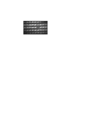
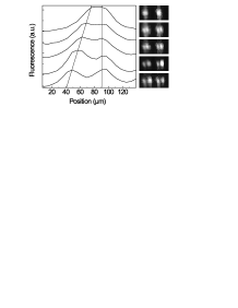
In addition to its scalability, our approach is especially suited to fulfill another requirement for the physical implementation of quantum information processing, namely the ability to selectively address, initialize, and read out individual qubits: The large lateral separation between the dipole traps enables us to selectively address the individual traps in a straightforward fashion. We demonstrate this by focusing a near-resonant laser beam onto one of the dipole traps for a few ms after the loading process is completed [28]. This heats the atoms out of the addressed dipole trap. As can be seen in Figure 3, no atoms are left at the site of the addressed dipole trap, while the atoms at the adjacent sites remain unaffected. By two-dimensional scanning of the addressing beam or by illuminating each lenslet individually with spatially modulated addressing light, every site can be addressed individually. This opens the possibility to selectively prepare and manipulate the qubits in the individual traps.
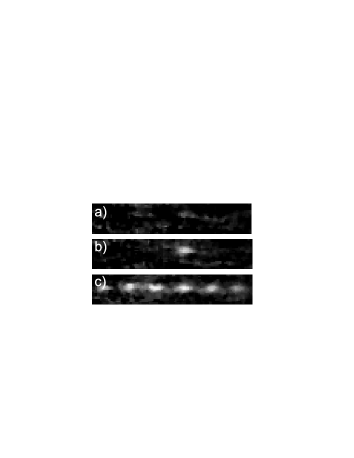
As a next step, we demonstrated the site specific and state selective initialization and readout of atomic
quantum states (Fig. 4). Here, we illuminate a one-dimensional atom array (analogous to Fig. 1 (b)) only with light resonant with the transition (i.e. the repump light switched off) during detection. Since the atoms are almost exclusively in the lower hyperfine groundstate after the loading phase, they do not scatter the detection light (Fig. 4 (a)) unless we actively pump them into the upper hyperfine groundstate during the time the atoms are stored in the dipole traps, i.e. prior to the detection phase (Fig. 4 (b),(c)). This has been done for one (Fig. 4 (b)) or, alternatively, all (Fig. 4 (c)) of the trap sites. This demonstrates the site specific and state selective initialization and detection capability of our approach.
While many of the advantages of our system result from the large lateral separation of the individual trap sites, it is also possible to actively control the distance between individual traps if smaller or adjustable distances are required, e.g. for quantum gate operations and the entanglement of atoms via atom-atom interactions. In our setup, this can be accomplished by illuminating one microlens array with two beams under slightly different angles (Fig. 5 (left)) [18, 21], which results in two interleaved sets of arrays of trapped atoms. Interference effects between the two laser beams are prevented by using orthogonal linear polariations. Figure 5 (right) shows two vertically displaced sets of arrays of trapped atoms with a mutual separation of 45 m. The separation only depends on the angle between the two laser beams and can easily be changed, especially to smaller values. By reducing the relative angle to zero, overlapping traps can be created. Figure 6 shows vertical cross-sections through one pair of dipole traps for different angles between the two laser beams and thus different site separations. We could also change the separation of the traps and thus move the atoms in one set of traps in real time by deflecting one beam with the help of a fast acoustooptical beam deflector. With this technique it should become possible to selectively prepare qubits at large distances, then decrease the distance for gate operations and entanglement via atom-atom interactions and then increase the distance again for the read out of the qubit states.
In order to demonstrate the full potential for quantum information processing, we evaluate the criteria given in [8] for our approach. Scalability, site specific and state selective initialization and readout, as well as the ability to change the separation of trapping sites at will are the most important advantages of our approach, and have been demonstrated in the previous sections. In addition, the concept presented here and the underlying technology fulfill the remaining two criteria, namely long relevant decoherence times and the availabilty of a universal set of quantum gates as well.
With the specific lens array of this work (beam waist 7 m) and a standard set of laser parameters (Ti:Sa laser, wavelength 825 nm, power per trap 50 mW) several tens of traps with radial vibrational frequencies of 10 kHz and a decoherence time (assumed to be limited by spontaneous scattering) of 50 ms can be obtained [18]. These parameters allow the implementation of collisional gates [4] with a decoherence time being at least 50 times longer than the gate time.
The full potential of our concept can be exploited by using available lens arrays optimized for large numerical
aperture: it has been shown experimentally [29] that beam waists below 1 m can be achieved with microlens arrays similar to the one used in this work. With standard laser parameters (wavelength 850 nm, power per trap 1 mW) radial vibrational frequencies of 50 kHz and decoherence times of 150 ms can be obtained. This allows the implementation of various types of quantum gates [4, 6, 7]. Due to its potentially short gate times and its insensitivity to the temperature of the atoms and to the variations in atom-atom separation, the Rydberg gate of [6] deserves specific attention: Using the parameters and scaling laws of [6], for atoms in microlens dipole traps with a waist and a respective minimum trap separation of 1 m, a gate time of about 1 s can be achieved. This gate time is 20 times shorter than the oscillation period and times shorter than the decoherence time, giving favorable experimental conditions. Further evidence for the potential of this approach can be drawn from the fact that this array of 1 m-waist dipole traps represents a 2D extension of the dipole trap demonstrated in [21]. For this trap a detailed investigation [30] gives proof for the feasability of Rydberg gates and explicitly shows that for trap separations of 1 to 5 m, gate times of 1 to 10 s are possible.
We conclude this discussion by pointing out that since our dipole trap arrays can give the same trap parameters as single dipole traps or standing wave dipole potentials, the single atom loading schemes experimentally demonstrated in [21] and [25] can be extended to our configurations in a straightforward fashion. In addition, with the achievable vibrational frequencies being larger than the recoil frequency, sideband-cooling of atoms to the vibrational ground state of the trap arrays should be possible. Finally, the demonstration of the loading of periodic dipole potentials with single atoms from a Bose Einstein condensate [31] might allow an extemely efficient means of single atom loading into vibrational ground states of our trap arrays.
This work is supported by the SFB 407 and the program Quanteninformationsverarbeitung of the Deutsche Forschungsgemeinschaft as well as by the program ACQUIRE (IST-1999-11055) of the European Commission.
REFERENCES
- [1] A.M. Steane, Rep. Prog. Phys. 61, 117 (1998); D. Bouwmeester, A. Ekert, and A. Zeilinger (ed.), The Physics of Quantum Information, Springer, Berlin (2000); Special Issue of Fortschritte der Physik 48 (2000).
- [2] C. Monroe et al., Phys. Rev. Lett. 74, 4011 (1995); C.A. Sackett et al., Nature 404, 256 (2000).
- [3] E. Hagley et al., Phys. Rev. Lett. 79, 1 (1997); A. Rauschenbeutel et al., Phys. Rev. Lett. 83, 5166 (1999).
- [4] D. Jaksch et al., Phys. Rev. Lett. 82, 1975 (1999); T. Calarco et al., Phys. Rev. A 61, 022304 (2000).
- [5] G.K. Brennen et al., Phys. Rev. Lett. 82, 1060 (1999).
- [6] D. Jaksch et al., Phys. Rev. Lett. 85, 2208 (2000).
- [7] E. Charron, E. Tiesinga, F. Mies, and C. Williams, Phys. Rev. Lett. 88, 077901 (2002).
- [8] D.P. DiVincenzo, Fortschr. Phys. 48, 9 (2000).
- [9] for ATom Optics with MICroStructures.
- [10] J.D. Weinstein and K.G. Libbrecht, Phys. Rev. A 52, 4004 (1995); J. Schmiedmayer, Eur. Phys. J. D 4, 57 (1998); E.A. Hinds and I.G. Hughes, J. Phys. D 32, R119 (1999).
- [11] J. Reichel, W. Hänsel, and T.W. Hänsch, Phys. Rev. Lett. 83, 3398 (1999); W. Hänsel, J. Reichel, P. Hommelhoff, and T.W. Hänsch, Phys. Rev. Lett. 86, 608 (2001); W. Hänsel, P. Hommelhoff, T.W. Hänsch, and J. Reichel, Nature 413, 498 (2001).
- [12] D. Müller et al., Phys. Rev. Lett. 83, 5194 (1999).
- [13] N.H. Dekker et al., Phys. Rev. Lett. 84, 1124 (2000).
- [14] M. Key et al., Phys. Rev. Lett. 84, 1381 (2000).
- [15] R. Folman et al., Phys. Rev. Lett. 84, 4749 (2000); D. Cassettari et al., Phys. Rev. Lett. 85, 5483 (2000).
- [16] H. Ott et al., Phys. Rev. Lett. 87, 230401 (2001).
- [17] P. Engels, W. Ertmer, and K. Sengstock, submitted.
- [18] G. Birkl, F.B.J. Buchkremer, R. Dumke, and W. Ertmer, Opt. Comm. 191, 67 (2001).
- [19] F.B.J. Buchkremer et al., Laser Physics 12, 143 (2002).
- [20] for an overview see R. Grimm, M. Weidemüller, and Y.B. Ovchinnikov, Adv. At. Mol. Opt. Phys. 42, 95 (2000).
- [21] N. Schlosser, G. Reymond, I. Protsenko, and P. Grangier, Nature 411, 1024 (2001).
- [22] D.Boiron et al., Phys. Rev. A 57, R4106 (1998).
- [23] S.J.M. Kuppens et al., Phys. Rev. A 62, 013406 (2000).
- [24] Z. Hu and H.J. Kimble, Opt. Lett. 19, 1888 (1994); F. Ruschewitz et al., Europhys. Lett. 34, 651 (1996); D. Frese et al., Phys. Rev. Lett. 85, 3777 (2000).
- [25] S. Kuhr et al., Science 293, 278 (2001).
- [26] We measure this frequency by parametrically heating the atoms and observing the number of remaining atoms.
- [27] M.D. Barrett, J.A. Sauer, and M.S. Chapman, Phys. Rev. Lett. 87, 010404 (2001).
- [28] R. Scheunemann, F.S. Cataliotti, T. W. Hänsch, and M. Weitz, Phys. Rev. A 62, 051801 (2000).
- [29] T. Hessler et al., Pure Appl. Opt. 6 673 (1997).
- [30] I.E. Protsenko, G. Reymond, N. Schlosser, and P. Grangier, accepted for publication in Phys. Rev. A.
- [31] M. Greiner, O. Mandel, T. Esslinger, T. W. Hänsch, and I. Bloch, Nature 415, 39 (2002).