The breakdown flash of Silicon Avalance Photodiodes – backdoor for eavesdropper attacks?
submitted to J. Mod. Opt.)
Abstract
Silicon avalanche photodiodes are the most sensitive photodetectors in the visible to near infrared region. However, when they are used for single photon detection in a Geiger mode, they are known to emit light on the controlled breakdown used to detect a photoelectron. This fluorescence light might have serious impacts on experimental applications like quantum cryptography or single-particle spectroscopy. We characterized the fluorescence behaviour of silicon avalanche photodiodes in the experimentally simple passive quenching configuration and discuss implications for their use in quantum cryptography systems.
1 Introduction
For a long time, silicon avalanche photodiodes (APD) have been used for single photon detection in the near-infrared region[1, 2] because of their high quantum efficiency and low dark count rate. These properties are particularly important for quantum cryptography[3, 4, 5, 6], where a huge yield of secure bits and a low signal/noise ratio is crucial.
To obtain a single photon counting behaviour, the avalanche diode is operated in an all-or-nothing counting mode similar to the way Geiger detectors are used in nuclear physics for particle counting. In this so-called Geiger mode, the diode is reversely biased above the breakdown voltage such that a single photoelectron can generate a self-sustaining discharge. The discharge current is used as an indicator for the generation of a photoelectron and thus of an absorbed photon. Thereby, a timing accuracy better then 60 ps has been achieved[7].
It has been observed previously that the avalanche of charge carriers is accompanied by photon emission[8]. Although this light emission is not very strong, in several single photon counting applications it may have serious impacts on the experiment. In quantum cryptography, for example, such a light emission might enable an external observer to gain information of a photo detection event on the receiver side, opening a possible eavesdropping back door to an otherwise secure communication channel. Another experimental situation in which this photoemission has to be considered are photon correlation measurements, as they are performed in single atom or molecule spectroscopy. In a typical Hanburry-Brown–Twiss configuration, two photodetectors are looking onto a faint light source, and one has to ensure that light emitted in the breakdown flash of one photodiode is not causing artificial photo events in the second photodetector due to residual crosstalk between the two photodetectors[9, 10, 11]. It is therefore important to know the photoemission characteristics of that breakdown photoemission to avoid crosstalk with the light to be detected. In this paper, we describe our investigation of the temporal and spectral distribution as well as the absolute amount of light emitted during a detection event.
2 Photodiode operation
A photodetection process is initiated by a photoelectron created after absorption of a photon in a reverse-biased -junction. This electron is accelerated into a highly doped region where an avalanche of charge carriers is triggered. In single photon counting mode, the bias voltage exceeds the breakdown voltage of the diode, meaning that once an avalanche has been triggered, it is self-sustaining as long as the external voltage exceeds the breakdown threshold. To avoid the thermal damage of the diode and to bring it back into a state ready for a subsequent photoelectron detection, the avalanche has to be quenched. This is done by lowering the reverse bias voltage across the diode for a certain time. After allowing all charge carriers to recombine and thus bringing the diode into an insulating state again, a full photodetection cycle is finished and the diode is ready for the next event.
The usual configurations for that procedure are referred to passive and active quenching[12]. In passive quenching, the diode is reverse-biased via a low-current network (e.g. a large resistor ) such that the discharge current triggered by a photoelectron avalanche causes a voltage drop, reducing the voltage across the diode below the breakdown voltage (see figure 1). Then, the junction capacity has to be recharged again to the full reverse bias voltage. With usual passive quenching configurations, a recharge time on the order of a microsecond is achieved. To obtain a faster recharge and thereby a shorter dead time, active quenching techniques have to be used[7]. Yet, the discharge current and thus the breakdown flash should not depend on the quenching configuration.

In our experiments, we used an APD with an integrated two stage thermoelectric cooler, type C30902-SDTC from Perkin-Elmer. The diodes have a circular active area of 0.5 mm diameter, and are accessible through a transparent window. They are mounted in modules together with a high voltage supply, a discriminator to generate standard NIM pulses and a temperature controller for the peltier element[13]. We use a current limiting network instead of a quenching resistor, a measurement resistor of and a reverse bias voltage of V at a temperature of C, which is approximately 20 V above the breakdown of the APD. According to the manufacturer, the diodes are supposed to show a single photon detection efficiency of up to % at a wavelength of 800 nm[14], depending on operating conditions.
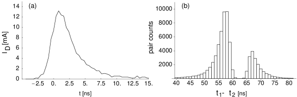
The discharge current we measured under these conditions is shown in figure 2a. It reflects an exponential decay, convoluted with a Gaussian distribution. From this measurement, we obtain a total charge of
released during a diode breakdown. From that value, we deduce a parasitic capacity of
assuming that during breakdown, most of the current through is supplied by , and not by the biasing network.
3 Absolute photoemission rate
To determine the amount of light emitted during a breakdown cycle, we used an optical arrangement sketched in figure 3. The active area of an APD module is imaged with a lens mm onto a second APD, , with a demagnification of 2 (corresponding to distances of mm and mm, respectively). This ensured that light emitted from all parts of the active area of diode could reach the active area of even for imperfect alignment. To define the solid angle of light collected from diode , we used an aperture with a diameter of 3 mm (and 5 mm in a second experiment) at a distance of mm from the diode. The corresponding solid angles are sr and sr, respectively.
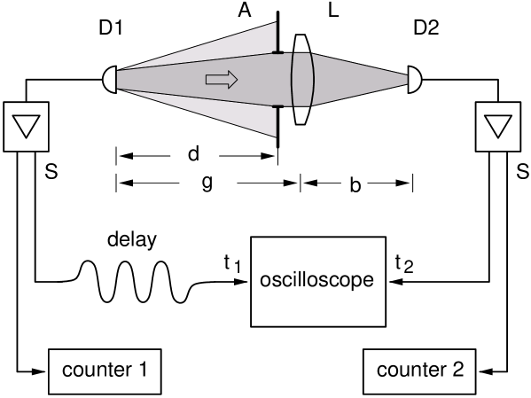
The NIM pulses were sent both to PC-card based counters, and for timing analysis to a digital oscilloscope (LeCroy LC574A). Using a pair trigger feature together with an auxiliary delay line of 63 ns, we collected coincidence events of the two detectors and histogrammed their time differences in an interval of -40 ns to +60 ns with a resolution of a few 100 ps.
To measure only the light emitted by the diode , we lowered the ambient light such that registered a count rate of cps. This is only moderately larger than the dark count rate (approximately 500 cps) and ensures that scattering of external light to the second diode is minimal. With the optical path open to the second diode and an aperture diameter of 3 mm, we observe a count rate from diode of cps. Finally, only pair events are selected which ensures that only the properties of the breakdown flash were analysed.
A histogram of time differences for double photo events is shown in figure 2b. One can clearly recognize two peaks, the left one ( ns) corresponding to photo events registered in detector after a discharge of detector , and the right one corresponding to the reverse process. The asymmetry in the amplitudes of the two peaks can be explained by the asymmetry in the imaging optics, as the aperture is not located exactly at the lens position, and/or by a difference in the amount light produced by the two diodes. Each peak shows a rise time between 1 and 2 ns, and an exponential decay, probably following the discharge current of the diode. The distribution of each peak of time differences in figure 2b has the same temporal pattern as the discharge current shown in figure 2a.
We modeled a higher resolution histogram of the first peak of by a convolution of an exponential decay with a time constant and a Gaussian distribution with a variance . Using the model function
where is a step function, we obtain fit values of ns and ns. The actual shape of this distribution is determined by the discharge network.
Integration over the pair distribution from ns to 62 ns leads to a rate of for photo events of detector induced by breakdown events of ; the accidental count rate for that time window,
is negligible. With the breakdown rate of and the captured solid angle , and assuming isotropic emission of the fluorescence light, we obtain a differential breakdown emission intensity of
for each detected breakdown of the diode . From a similar measurement with an aperture diameter of 5 mm, we found a value of photons/sr. Within the accuracy of the alignment of the photodetectors and the assumption of isotropy of emission, these two values are compatible. However, these values do not contain a detection efficiency yet. Because this detection efficiency varies with the wavelength (and has a maximum of at nm[14]), an estimate of total rate can only be given with a knowledge of the spectral distribution.
4 Spectral distribution of the breakdown emission
In order to evaluate possible countermeasures in experiments sensitive to the breakdown light emission of an APD, we measured the spectral distribution of that light. Therefore, we used again a setup of two single photon counting APDs looking at each other, where we inserted a reflection grating as a tunable filter in the optical path as shown in figure 4. The active area of the diode under investigation, , was placed in the focal plane of a lens ( mm) to collimate the light emitted in a diode breakdown. The first diffraction order of a blazed grating (1200 lines/mm) was focused with another lens onto the second APD, , acting as a photon detector. At a wavelength of 632 nm, we thereby obtain a wavelength resolution of approximately 3.3 nm FWHM; we adjusted the transmitted wavelength by turning the grating.

Again, we identify photons from the breakdown flash in by looking for coincidences of detector events in and . We have chosen a coincidence time window of ns after a breakdown of . In the experiment, we recorded the number of coincidence events, , and events of the individual detectors for an integration time . To obtain acceptable signal levels, we exposed detector to a raised level of background light, causing breakdown rates of . The corresponding count rate of detector was in the range of . The number of coincidence events varied form 300 to 1100 counts over the recording periode.
We correct for accidental coincidences and fluctuations in the breakdown rates of APD , and obtain a normalized spectral distribution from our experimental data using the expression:
The spectrum obtained after an integration time of sec per point is shown in figure 5, using a normalization constant of .
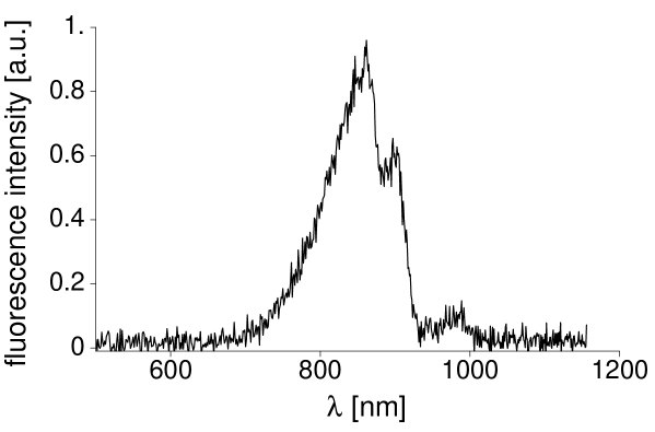
One can identify a spectral emission ranging from 700 nm to 1000 nm, with a maximum at 860 nm, two sharp edges at 872 nm and 913 nm, respectively, and two weaker maxima at 900 nm and 980 nm, respectively. This structure is a product of the emission spectrum of the breakdown light, the transfer function of our spectrometer setup and the spectral sensitivity for photo detection of the second avalanche diode . While the transmission of the spectrometer is reasonably flat over the investigated region, the main deviation between the measured and the emitted spectrum can be attributed to the wavelength dependency of the quantum efficiency of detector , which, according to the manufacturer, has a smooth drop-off from 70% to 8% in the range of to 1000 nm[14]. However, the key structures of the spectrum obtained are not an artefact of the detection efficiency, and are characteristic to the generation process of the emitted light.
5 Impact of photoemission on a quantum cryptography system
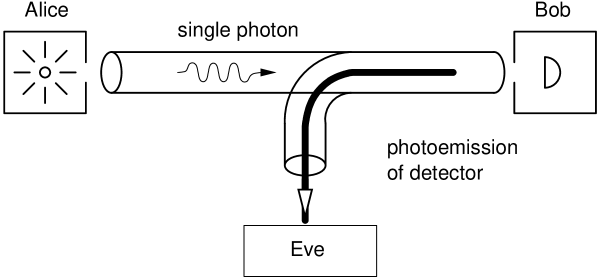
In our experiments, we tried to quantify the photoemission on breakdown of silicon avalanche photodiodes in Geiger mode. This photoemission may allow a possible eavesdropper in a quantum cryptography application to gain information of the outcome of a measurement simply by looking at this photoemission, as sketched in figure 6. It therefore has to be ensured that the amount of light leaking back to a possible eavesdropper is small in order to limit its knowledge on the outcome of the single particle measurement by Bob.
To minimize the amount of light generated in the first place, the capacity should be reduced to a minimum. This technique, however, quickly reaches a limit with currently available photodiode packages.
Another measure to reduce the emitted light would be the use of optical filters, blocking the spectral range of 700-1000 mn in which photoemission occurs. However, this technique is restricted to cases where the wavelength of the transmitted light is outside that range. This is the case with recently developed diamond-based single photon sources[9], or using shorter wavelength laser diode emission[15]. For systems using laser diodes around 850 nm exploring an absorption minimum in optical fibers[16], this technique would require narrow band interference filters around the emission wavelength of the diodes. Then, the possible leakage of information to an eavesdropper can be made negligibly small, too.
Additionally, spatial filtering may be used to block light propagating back the quantum channel. Assuming that the photoemission light is emitted without spatial coherence across the photo detection surface, and that light to be detected is coming out of a single spatial mode from an optical fiber or an equivalent spatial mode filter in a free space arrangement, the back-propagating light is reduced.
To estimate the fraction of light coupled back, we first consider the breakdown flash brilliance (i.e., the number of photons emitted per surface area and solid angle) for each photon detection event. From our measurements, we find
where is the sensitive area of the photodiode. The number of photons collected from such an incoherent source into a single spatial mode, characterized e.g. by a Gaussian beam waist and a corresponding divergence , is given by:
Integrating over a wavelength range from 700 nm to 1050 nm, we obtain a numerical value of photons coupled into the single spatial mode of the quantum channel for a detection event. This value is independent of the detailed structure of the coupling optics as long as reciprocal optical elements are used. It is also only a lower limit obtainable with a similar photodetector, since we have not taken into account the quantum efficiency of the photo detector.
To correct for the quantum efficiency and to estimate the real number of photons coupled back into the quantum channel, we use the measured spectral distribution and a detection efficiency (i.e., the product of photoelectron generation probability given by the manufacturer and the photoelectron detection efficiency of .55 at 20 V above breakdown) obtained from the manufacturer. Then, we numerically derive a correction factor given by the expression:
For a wavelength range from 700 nm to 1050 nm, we obtain a numerical value of . With this factor, we end up with a corrected numerical value of photons coupled back into the single spatial mode of a quantum channel.
6 Summary
To summarize, we quantified the photoemission behavior of a silicon avalanche diode during a breakdown, such as induced by a detection event of a single photon, we found an emission spectrum ranging from 700 nm to 1000 nm, and estimated the possible leak of information to a possible eavesdropper due to this effect. Whereas this emission might have to be considered for single atom and molecule spectroscopy, in quantum cryptography the backdoor for an eavesdropper can be closed by taking some care with spectral and spatial mode filtering. It remains to be investigated if photodiodes used for quantum cryptography systems[17] in the telecom wavelength range (1300 nm and 1550 nm) which are usually based on InGaAs or Ge, show a similar effect. With InGaAs being a direct semiconductor, one could expect it to be more likely for charge carriers to undergo radiative recombinations than in silicon or germanium, thus showing a stronger breakdown flash.
Acknowledgements
This work was supported by the European Union in the EQCSPOT project (EC28139) and the Deutsche Forschungsgemeinschaft.
References
- [1] R. Conradt, 1968, Z. f. Physik, 209, 445.
- [2] W. Haecker, O. Groetzinger, and M.H. Pilkhuhn, 1971, Appl. Phys. Lett., 19, 113.
- [3] H.-K. Lo, S. Popescu, and T. Spiller, 1998, Introduction to Quantum Computation and Information (Singapore: World Scientific).
- [4] D. Bouwmeester, A. Ekert, and A. Zeilinger, 2000, The Physics of Quantum Infotmation (Berlin: Springer Verlag).
- [5] An updated bibliography on quantum cryptography can be found at http://www.cs.mcgill.ca/crepeau/CRYPTO/Biblio-QC.html
- [6] H. Zbinden, H. Bechman-Pasquinucci, N. Gisin and G. Ribordy, 1998, Appl. Phys. B, 67, 743-748.
- [7] S. Cova, A. Longoni, and A. Andreoni, 1981, Rev. Sci. Instr., 52(3), 408.
- [8] J.G. Rarity, Private communication.
- [9] C. Kurtsiefer, S. Mayer, P. Zarda, and H. Weinfurter, 2000, Phys. Rev. Lett., 85, 290.
- [10] W. E. Moerner, and M. Orrit, 1999, Science, 283, 1670-1676
- [11] B. Lounis and W.E. Moerner, 2000, Nature, 407, 491-493.
- [12] R.G.W. Brown, R. Jones, J.G. Rarity and K.D. Ridley, 1987, Appl. Opt., 26, 2383.
- [13] P. Zarda, 1999, Quantenkryptographie – Ein Experiment im Vergleich. Diploma thesis, University of Innsbruck, Austria.
- [14] Data sheet for the C30902-SDTC diode module, supplied by Perkin-Elmer, formerly EG&G.
- [15] W.T. Buttler, R.J. Hughes, S.K. Lamoreaux, G.L. Morgan, J.E. Nordholt, and C.G. Peterson, 2000, Phys. Rev. Lett., 84, 5652.
- [16] S. Chingga, P. Zarda, T. Jennewein, and H. Weinfurter, 1999, Appl. Phys. B, 69, 389.
- [17] A. Muller, T. Herzog, B. Huttner, W. Tittel, H. Zbinden and N. Gisin, 1997, Appl. Phys. Lett., 70, 793-795.