Atom Optics with Microfabricated Optical Elements
Abstract
We introduce a new direction in the field of atom optics, atom interferometry, and neutral-atom quantum information processing. It is based on the use of microfabricated optical elements. With these elements versatile and integrated atom optical devices can be created in a compact fashion. This approach opens the possibility to scale, parallelize, and miniaturize atom optics for new investigations in fundamental research and application. It will lead to new, compact sources of ultracold atoms, compact sensors based on matter wave interference and new approaches towards quantum computing with neutral atoms. The exploitation of the unique features of the quantum mechanical behavior of matter waves and the capabilities of powerful state-of-the-art micro- and nanofabrication techniques lend this approach a special attraction.
I Introduction
The investigation and exploitation of the wave properties of atomic matter is of great interest for fundamental as well as applied research and therefore constitutes one of the most active areas in atomic physics and quantum optics. Profiting from the enormous progress in laser cooling [1], the field of atom optics has been established and research in this area has already led to many exciting results: Various types of atom optical elements (lenses, mirrors, beam splitters, etc.) [2] and atom interferometers [3] have been realized and precise atom interferometrical measurements of fundamental constants [4], atomic properties [5, 6, 7, 8], acceleration forces [9, 10] and rotations [11, 12, 13] have been performed. With the development of reliable sources for coherent matter waves such as Bose-Einstein condensates [14] and laser-like atom beams [15] this work is in the process of being extended towards improved measurement schemes based on the properties of many-particle wavefunctions [16].
As a consequence of all these developments, there is now a vast interest in compact and reliable atom optical setups which not only expand the applicability of atom optics in fundamental research, but also allow the technological implementation of atom optical measurement systems. A new approach to this challenge lies in the development of miniaturized and integrated atom optical setups based on microfabricated structures.
A number of groups have employed microfabricated mechanical structures [5, 17, 18, 19] for applications in atom interferometry and atom optics. While these elements have a number of promising features, integrated atom optical setups based on these structures still have to be developed. As an alternative approach, the trapping and guiding of neutral atoms in microfabricated charged and current carrying structures has been pursued in recent years [20, 21, 22, 23, 24, 25, 26, 27]. The simplicity and stability of these setups as well as the favorable scaling laws make them promising candidates for the miniaturization and integration of atom optical elements.
In this paper we introduce a new approach to generate miniaturized and integrated atom optical systems: We propose the application of microfabricated optical elements (microoptical elements) for the manipulation of atoms and atomic matter waves with laser light. This enables one to exploit the vast industrial and research interest in the field of applied optics directed towards the development of micro-optical elements, which has already lead to a wide range of state-of-the-art optical system applications [28, 29] in this field. Applying these elements to the field of atom optics, however, constitutes a novel approach. Together with systems based on miniaturized and microfabricated mechanical as well as electrostatic and magnetic devices, the application of microoptical systems will launch a new field in atom optics which we call ATOMICS for ATom Optics with MICro-Structures. This field will combine the unique features of devices based on the quantum mechanical behavior of atomic matter waves with the tremendous potential of micro- and nanofabrication technology.
II Microoptical Elements for Atom Optics
A special attraction of using microoptical elements lies in the fact, that most of the currently used techniques in atom optics as well as laser cooling are based on the optical manipulation of atoms. The use of microfabricated optical elements is therefore in many ways the canonical extension of the conventional optical methods into the micro-regime, so that much of the knowledge and experience that has been acquired in atom optics can be applied to this new regime in a very straightforward way. There are however, as we will show in the following, a number of additional inherent advantages in using microoptics which significantly enhance the applicability of atom optics and will lead to a range of new developments that were not achievable until now: The use of state-of-the-art lithographic manufacturing techniques adapted from semiconductor processing enables the optical engineer to fabricate structures with dimensions in the micrometer range and submicrometer features with a large amount of flexibility and in a large variety of materials (glass, quartz, semiconductor materials, plastics, etc.). The flexibility of the manufacturing process allows the realization of complex optical elements which create light fields not achievable with standard optical components. Another advantage lies in the fact, that microoptics is often produced with many identical elements fabricated in parallel on the same substrate, so that multiple realizations of a single conventional setup can be created in a straightforward way. A further attraction of the flexibility in the design and manufacturing process of microoptical components results from the huge potential for integration of different elements on a single substrate, or, by using bonding techniques, for the integration of differently manufactured parts into one system. No additional restrictions arise from the small size of microoptical components since for most applications in atom optics, the defining parameter of an optical system is its numerical aperture, which for microoptical components can easily be as high as NA=0.5, due to the small focal lengths achievable.
Among the plethora of microoptical elements that can be used for atom optical applications are refractive or diffractive microoptics, computer generated holograms, microprisms and micromirrors, integrated waveguide optics, near-field optics, and integrated techniques such as planar optics or micro-opto-electro-mechanical systems (MOEMS). Excellent overviews of microoptics can be found in [28, 29]. To our knowledge, of all these elements only computer generated holograms and phase gratings have been used in atom optics so far for guiding [30] and trapping [31, 32, 33] of atoms.
In this paper we give an overview of the novel possibilities arising for atom optics with the use of microfabricated optical elements. We show how all crucial components for miniaturized systems for atom optics, atom interferometry, and quantum information processing with neutral atoms can be realized with microoptical elements. We will present the key properties as well as the achievable parameter range of selected atom optical elements based on microoptical components and will discuss the advantages and new possibilities that arise with this novel approach.
III Optical Dipole Force and Photon Scattering
The optical manipulation of neutral atoms in most cases is based on the electric dipole interaction of atoms with laser light. It leads to spontaneous scattering of photons, which allows cooling, state preparation and detection of atoms and to an energy shift experienced by the atoms, which gives rise to the dipole potential.
For an understanding of the basic properties of both effects it is sufficient to assume the atom to act as a two-level system ignoring the details of its internal substructure [34]. A detailed treatment of the dipole force and the modifications arising for multi-level atoms can be found in [35, 36].
The rate of spontaneous scattering processes is given by
| (1) |
valid for negligible saturation () and large detuning . is the position dependent laser intensity, and are the laser frequency and the atomic resonance frequency respectively, and is the natural decay rate of the population in the excited state.
A conservative, non-dissipative force acting on the atoms is derivable from the dipole potential
| (2) |
again valid for () and . The direction of the dipole force depends on the sign of the detuning . The dipole force is attractive if the frequency of the laser light lies below an atomic resonance (, ”red detuning”), and repulsive if the frequency of the light lies above an atomic resonance (, ”blue detuning”). For typical experimental conditions, the detuning is much smaller than the atomic resonance frequency (). In this regime the dipole potential scales as , whereas the rate of spontaneous scattering scales as . If decoherence as caused by spontaneous scattering has to be suppressed the detuning should be chosen as large as possible.
It is the basic principle of the optical manipulation of atoms to create light fields with the appropriate intensity distribution at a suitable detuning. Microoptical systems are extremely well suited for this purpose since they allow the efficient and flexible generation of complex intensity distributions.
IV Multiple Atom Traps
Among the key elements in atom optics are traps for neutral atoms. Already very early in the development of this field, a simple atom trap based on the dipole potential of a focused red-detuned laser beam has been realized [37] and has remained an important element ever since [35]. This work has been extended to the generation of multiple dipole traps by the interference of multiple laser beams [31, 38].
A new approach arises from the application of one- or two-dimensional arrays of spherical microlenses for atom trapping (Fig. 1). Microlenses have typical diameters of ten to several hundreds of m. Due to their short focal lengths of typically 100m to 1mm, their numerical aperture can be easily as high as 0.5, resulting in foci whose focal size q (defined as the radius of the first minimum of the Bessel function which results from the illumination of an individual microlens with a plane wave [39]) can be easily as low as q=1m for visible laser light [40].
By focusing a single red-detuned laser beam with a spherical microlens array, one- or two-dimensional arrays of a large number of dipole traps can be created, in which single- or multiple-atom samples can be stored (Fig. 2).
Table I shows the properties of such dipole traps (m) for rubidium atoms, as an example of a frequently used atomic species, for various commonly used laser sources [39]. One can easily obtain an individual atom traps in a very compact setup with extremely low laser power or a large number (100 in the case of Table I) of atom traps of considerable depth with rather moderate laser power. The trap depth is significantly larger than the kinetic energy of the atoms achievable with Doppler cooling (0.141 mK for rubidium). The low rates of spontaneous scattering that are achievable with sufficiently far-detuned trapping light ensure long storage and coherence times, while the strong localization of the atoms in the Lamb-Dicke-regime [42] () strongly suppresses heating of the atoms and makes it possible to cool the atoms to the ground state of the dipole potential via sideband cooling in all dimensions. In this case the size of the atomic wavefunction reaches values that are significantly smaller than 100 nm, even approaching 10 nm in many cases, thus making microlens arrays well suited for the generation of strongly confined and well localized atom samples.
The advantages of trap arrays can, for example, be exploited for atom-interferometrical applications where it becomes possible to simultaneously perform a large number of measurements (thereby improving the signal-to-noise ratio) or to instantaneously measure the spatial variation of the property under investigation.
The lateral distances between the individual traps (typically 100 m) make it easy to selectively detect and address the atom samples in each dipole trap. While the natural way of addressing an individual trap consists in sending the addressing laser beams through the corresponding microlens, there are also more sophisticated methods possible, e.g. with a two-photon Raman-excitation technique as depicted in Fig. 2. Raman excitation has been applied frequently to create superposition states in alkali atoms [41] and relies on the simultaneous interaction of the atoms with two mutually coherent laser fields. For a sufficiently large detuning from the single photon resonance, only the atoms in the trap that is addressed by both laser beams are affected by them. By sending one Raman beam along a column and the other beam along a row of the lens array a specific superposition can be created for each individual trap, while unwanted energy shifts affecting the remaining traps can be easily compensated.
These factors open the possibility to prepare and modify quantum states in a controlled way (”quantum engineering”) in each trap, which is a necessary ingredient for parallelized atom interferometers and atom clocks but also for quantum computing, thus making this system also very attractive for quantum information processing applications (see section VII. below).
The manipulation of atoms with microlens arrays is extremely flexible: It is easily possible to temporarily modify the distances between individual traps if smaller or adjustable distances between traps are required. This can be accomplished either by using two independent microlens arrays which are laterally shifted with respect to each other or by illuminating a microlens array with two beams (possibly of different wavelength) under slightly different angles (Fig. 3), thereby generating two distinct sets of dipole trap arrays. Their mutual distance can be controlled by changing the angle between the two beams. With a fast beam deflector, this can be done in real-time during the experiment.
V Atomic Waveguides
Many of the future applications of cold atomic ensembles rely on the development of efficient means for the transport of atoms. Several configurations for one-dimensional guiding of atoms have been studied in recent years. The guiding of atoms along the dark center of blue-detuned Laguerre-Gaussian laser beams has been achieved [30, 43]. Hollow core optical fibres have been used to guide atoms [44]. Using magnetic fields, atoms have also been guided along current carrying wires [45, 46], above surface mounted current carrying wires [22, 23, 24, 25, 26] and inside hollow-core fibres with current carrying wires embedded in the fibre [27].
For atom guiding too, novel approaches arise from the application of microfabricated optical elements. By using cylindrical microlenses or microlens arrays, for example, one-dimensional guiding structures for atoms can be developed (Fig. 4). The light that is sent through such a system forms a single line-focus or a series of parallel line-foci above the lens system.
By focusing a red-detuned laser beam with homogeneous intensity distribution an atomic waveguide is formed. Atoms are confined in the two dimensions perpendicular to the lens axis but are free to propagate along the axis. Since the manufacturing process is identical to that of spherical microlens arrays, cylindrical microlenses can be manufactured with similar dimensions and numerical apertures so that the focal size of the line foci again can be as low as q=1 m for visible light. Due to the flexibility of the fabrication process, rather complicated waveguide geometries can be achieved. The shape of the lens can be curved (Fig. 5 (a)) creating a bent waveguide or the lens can even be circular (Fig. 5 (b)) resulting in a closed one-dimensional potential minimum which can be used as a miniaturized storage ring or resonator for atomic matter waves.
Table II shows the properties of a 10mm long waveguide for m, rubidium atoms and various commonly used laser sources. Waveguides with potential depths comparable to the kinetic energy achievable with Doppler cooling can easily be created. They are well suited for generating single or integrated structures for guiding atoms and atomic matter waves in compact atom optical systems although other guiding structures [22, 23, 24, 25, 26, 27, 30, 43, 44, 45, 46] might be more favorable for guiding atoms over distances that are larger than several cm.
Of specific interest for atom optical applications are single-mode waveguides for atomic matter waves since the development of atom interferometers based on guided atoms and the coherent transport of Bose-Einstein condendates or atom laser outputs are strongly profiting from single-mode guiding. For this purpose it is essential to have the atoms confined in the Lamb-Dicke regime. As can be seen from Table II, with the exception of the waveguide, the oscillation frequencies are comparable to (in the z-direction) or significantly larger than (in the r-direction) the recoil frequency (= for rubidium). Thus, single-mode guiding with sufficiently low probability of excitation of the atomic wave packets to higher vibrational states is achievable with very low rates for spontaneous scattering.
In addition to microfabricated cylindrical lenses, there exist other microoptical techniques which can be applied to create waveguide structures for atoms. One of the most promising candidates for large scale integration of atomic waveguides is the application of planar optical waveguide structures [28, 29]. The basic concept is to implement spatial variations in the index of refraction near the surface of an optical substrate in order to induce total internal reflection at the boundaries of these regions and thus spatially localize the light field. The structured light field evanesces from the surface and can be used to create complex two-dimensional patterns of dipole potential wells and barriers parallel to the surface of the substrate. Additional confinement of the atoms in the direction perpendicular to the surface can be achieved for example by a standing light wave pattern created by reflecting a laser beam from the surface [47] or by an additional magnetic field creating a two-dimensional magnetic waveguide [48].
VI Beam Splitters and Interferometers
Significant applications of microfabricated atom-optical and atom-interferometrical devices arise when the key elements for more complex systems can be demonstrated and their integration can be realized. One of the key elements in this respect is a beam splitter for atomic matter waves. Beam splitters based on microfabricated current carrying wires have already been demonstrated [49, 50]. Microoptical beam splitters on the other hand, can be based on a straightforward extension of the microoptical waveguides discussed above. The demonstration of coherent beam splitting will be the next step for all of these devices (see also [51]).
Fig. 6 shows a beam splitter based on the combined light fields of two curved cylindrical microlenses. Each microlens is illuminated by a light beam under a different angle (Fig. 6 (b)). This causes the laser foci to be laterally displaced with respect to the center of the lenses. By an appropriate choice of the displacements, the guiding potentials of the waveguides can be made to overlap at the closest approach making the full structure to act as a beam splitter. With an appropriate choice of the polarization states of the two light fields, interference effects can be avoided. Input wave packets propagating along one of the waveguides are split into up to four output wave packets propagating along both waveguides in both directions. Since the full structure is completely based on conservative potentials, the beam splitting process should be non-dissipative, so that coherent beam splitting of atomic matter waves is achievable. A detailed discussion of the properties of this beam splitter is published elsewhere [51].
This beam splitter can easily be extended to a microfabricated interferometer for atomic matter waves: Combining two beam splitters creates a Mach-Zehnder-type interferometer (Fig. 7). The two wave packets propagating along the output waveguides of the first beam splitter can be recombined in a second beam splitter and made to interfere.
As shown in section V, with typical laser powers guiding of ultracold atomic matter waves along microlens-based waveguides over distances of several 10 mm is possible. This allows the realization of interferometers with an enclosed area of at least 1 which represents the state-of-the-art for atomic matter wave interferometers [13]. With microfabrication such a large area can be achieved in a system with dimensions that are significantly smaller than those of setups based on conventional methods. This presents a major step towards miniaturization of atom-interferometrical devices and promotes the wide applicability of sensors based on atom interferometry. The Mach-Zehnder interferometer presented in Fig. 7 can be used as a Sagnac interferometer for measuring rotational motion with extremely high sensitivity.
VII Quantum Information Processing
The microoptical elements discussed so far lend themselves also particularly well to quantum information processing [52] exploiting the fact that qubits can be represented by superpositions of internal and external states of atoms in a straightforward fashion. Inherently an approach based on microoptical systems addresses two of the most important requirements for the technological implementation of quantum information processing: parallelization and scalability. In addition, the possibility to selectively address individual qubits is essential for most schemes proposed for quantum computing with neutral atoms. As a first and easily achievable implementation, single qubits associated with long-lived internal states can be prepared and rotated in each individual trap of a two-dimensional dipole trap array (Fig. 2), stored and later read out again. Thus, this device can serve as a quantum state register. The low rates of spontaneous scattering that are achievable in far-detuned microtraps (see Table I) ensure the long coherence times that are required for succesful quantum information processing.
An important step towards a functioning quantum computer is the implementation of two-qubit gates. Due to their inherent features, microoptical devices are also well suited for this purpose. Considering, for example, quantum gates based on dipole-dipole interactions between atoms [53] all requirements are fulfilled in the configuration depicted in Fig. 3. Atoms localized in neighboring traps can be brought close to each other with a definable separation in the single-micron range and for a predefined duration, in order to collect the required phase shift. Especially well suited is this configuration also for quantum gates based on the dipole-dipole interaction of low-lying Rydberg states in constant electric fields, as proposed in [54].
Another possible implementation of quantum gates relies on the entanglement of atoms via controlled cold collisions [55] which can be realized in configurations that consist of a combination of spherical and cylindrical microlenses. As depicted in Fig. 8, the two-dimensional array of dipole traps shown in Fig. 2 can be combined with waveguides created by cylindrical lens arrays. The result is a network of interconnected dipole traps. This network can be utilized for the transport of atoms from one potential well to the other by applying additional laser fields. Since this transfer can be made state dependent - via the detuning of the transport light fields - this mechanism can be utilized for letting the atoms collide state-dependently, thereby allowing the implementation of controlled-collision quantum gates.
A further, very powerful method for two- or multiple-atom entanglement is based on the extremely strong coupling between atoms and single-mode light fields exploited in cavity-QED experiments [56, 57]. Fig. 9 shows a configuration where two atoms trapped in microoptical dipole traps based on spherical microlenses (Fig. 2) can interact with the whispering-gallery mode of a dielectric microsphere [58, 59, 60, 61]. The interaction with this mode, which can have a quality factor Q as high as represents an extremely fast method of atom entanglement.
Due to their large numerical aperture, microoptical components can also be used for efficient spatially resolved read-out of quantum information of atoms (Fig. 10). In most cases the state of a qubit is recorded by exciting the atom state-selectively with resonant light and collecting the fluorescence light. Microoptical components can be used for the collection optics. Furthermore, the optical detection of quantum states with microoptical components is not restricted to optical trapping structures (Fig. 10 (a)) but can also be combined with the miniaturized magnetic and electric trapping structures (Fig. 10 (b)) currently investigated by a number of groups [22, 23, 24, 25, 26, 27].
Thus, all steps required for quantum information processing with neutral atoms - i.e. the preparation, manipulation and storage of qubits, entanglement, and the efficient read-out of quantum information - can be performed using microfabricated optical elements.
VIII Microstructured Atom Sources
An important step towards fully integrated atom optical setups is the development of miniaturized sources of ultracold atoms. Again, microoptical components can be used to achieve this goal, once more profiting from the fact that most of the preparation techniques for atom samples are based on optical manipulation. In this section we describe a miniaturized version of the ”workhorse” in atom optics, the magneto-optical trap (MOT). Our approach for developing a compact MOT is based on the concept of ”planar optics” [28, 29].
In planar optics, complex optical systems are integrated monolithically on a substrate. The optical path is folded in such a way, that the light propagates along a zig-zag path inside the substrate and the light is manipulated by reflective optical components (mirrors, beam splitters, lenses, retarders, etc.) that are mounted on or machined into the surface of the substrate. Planar optical systems can be used for a broad range of atom optical applications including atom traps, waveguides, beam splitters, interferometers, networks, and systems for quantum information processing.
As one example of an integrated system based on planar optics, Fig. 11 depicts an integrated MOT. The optical components are mounted on two parallel substrates, separated by several mm or cm. The trapping light is coupled into the lower substrate and split into four beams, which, after passing through quarter-wave plates, intersect a few mm or cm above the substrate. The beams enter the upper substrate and are retroreflected after double-passes through quarter-wave plates. Between the two substrates microfabricated coils for the MOT quadrupole fields are mounted. At the center of the upper substrate a two-dimensional microlens array is included indicating the possibility of integrating the MOT with other microoptical elements. The small size of an integrated MOT configuration will limit the achievable atom number. With a beam diameter of several mm still several atoms should be trapped imposing no limitations for most of the applications discussed here.
IX Integration
The huge potential for integration of microoptical components can be used for a large variety of further atom optical purposes. Since the same techniques are applied for the fabrication of microoptical components and microstructured wires on surfaces, microoptical components can be easily combined with the magnetic and electric strucures of [20, 21, 22, 23, 24, 25, 26, 27] (e.g., as shown Fig.10 (b)). In addition, microfabricated atom-optical components can be integrated with optical fibres and waveguides so that the results of atom optical operations after being read-out by detection of the scattered light can be further processed by optical means. Another canonical extension is given by the integration of microoptical components with optoelectronic devices such as semiconductor laser sources and photodiode detectors. In this case, the communication with the outside world can take place fully electronically, with the required laser light created in situ and the optical signals converted back to electrical signals on the same integrated structure.
The richness of the available microfabrication technologies manifests itself in another approach to integration based on micro-opto-electro-mechanical systems (MOEMS) [28, 29, 62]. The defining purpose of these elements is to steer optical signals by microfabricated mechanical components which can be positioned electrically. Significant research effort has been directed towards the development of microfabricated opto-electro-mechanical components. With these elements fast switching and steering of laser beams becomes possible, so that complex spatial and temporal field patterns can be generated.
X Experimental Considerations
One important question that has to be addressed in view of the applicability of microoptical systems is how to load atoms into these microscopic traps and guides. Since the distance of the substrate carrying these structures to the atom sample for microoptical components is typically given by the focal length of several hundred m, loading of atoms should be easier than for microstructured systems based on the magnetic or electrostatic fields [20, 21, 22, 23, 24, 25, 26, 27] with distances on the order of 1 to 100 m. Loading into these magnetic microstructures has been achieved by modified MOT configurations and a transfer of the atoms to the substrate’s surface [22, 23] or by elaborate schemes to transfer the atoms to the surface [24, 25, 26, 27]. Similar solutions can be applied for systems based on microoptical elements since for small microoptical structures the laser beams for a MOT can be reflected off or transmitted by the structure carrying substrate with only minor perturbations of the MOT.
In addition, further loading techniques are available for optical microstructures: 1) Microoptical systems can be positioned several mm or even cm away from the MOT with the focal plane being imaged into the center of the MOT without significant degredation thus significantly enlarging the distance between the MOT and the structure carrying substrate. 2) The compact size of microoptical elements together with the transmittivity of the supporting substrate should enable one to position the substrate directly at the required distance from the MOT by simply shining parts of the MOT beams through the transparent substrate, thus allowing to capture atoms in the micropotentials in situ or, if necessary, after a small lateral translation at the end of the MOT phase.
In the long term, the canonical way to load atoms into these devices will be based on microstructured atom sources as described in section VIII., or on the transfer of atoms collected in a separated MOT and then transferred into the microfabricated atom-optical systems by guiding them with laser beams, magnetic fields or inside guiding structures based on some of the systems discussed above.
Another point that has to be considered, which is also present for magnetic and electrostatic structures, are the possible side-effects of stray fields. In the case of microoptics, especially for more complex and integrated devices, unwanted scattering, diffraction, and reflection of the light fields has to be suppressed. Due to the small distance of the atoms from the structure carrying substrates these problems might be more severe than for conventional optical components. Measures have to be taken to minimize these side effects and to absorb or guide the light fields away from the atoms after their desired interaction. Techniques for this purpose (e.g., beam-dumping) are, however, well established in standard optics and can also be applied for the structures discussed here. In addition, similar questions arise for standard applications of microoptical components in applied optics and the design of the components is optimized to reduce these effects.
For all of the configurations presented above, fluctuations of the depth, shape, and position of the trapping potentials have to be sufficiantly small. This is especially true for applications requiring a preservation of coherence. The effects of beam jitter, intensity fluctuations, etc. have to be investigated and minimized if necessary although integrated microoptical systems have the advantage of being instrinsically stable.
Finally, the availability of microoptical components has to be discussed. Standard components such as arrays of spherical or cylindrical microlenses are commercially available. Optimized or highly integrated components can be custom-made with available micro- and nanofabrication technology by several companies. An excellent overview of the state-of-the-art of microoptics design and manufacturing can be found in references [28, 29].
XI Conclusion
In this paper we have shown that by using microoptical components one can create
a variety of powerful configurations with many applications in the fields of atom optics, atom
interferometry, and quantum information processing with neutral atoms. These applications
hugely benefit from the many inherent advantages of microoptical
components.
- Importance of optical methods: In atom optics, atom
interferometry and quantum information processing with neutral atoms, the initial preparation
of atom samples, the preparation and
manipulation of superposition states and qubits and the readout of results are usually
achieved by optical
means.
For this reason the application of state-of-the-art microoptical systems for the optical
manipulation of atoms is the canonical extension of today’s experimental techniques into the
microregime.
Another potential advantage
of the application of microoptical systems relates to
the fact that in the microscopic magnetic and electric structures of
[20, 21, 22, 23, 24, 25, 26, 27]
the atoms have to be very close
(typically 1-100m) to a room-temperature metallic surface in order to ensure the large
potential depths required for the envisaged applications. As calculated in
[63], this can significantly reduce the trapping and coherence times due to the
coupling of the atoms to fluctuating magnetic fields in the vicinity of the surface.
In the case of
microoptical systems this problem is insignificant, since for glass substrates the
effects of magnetic fluctuations are significantly reduced, and since the distance of the atoms
to the surface is
much larger (typically several hundreds of m) for the same potential depths.
Optical trapping potentials on the other hand, intrinsically suffer from possible losses of
coherence due to spontaneous scattering of photons. While this effect can in principle
be suppressed by employing light fields with sufficiently large detuning
the final limit of the trapping and coherence
times in optical traps remains to be investigated.
- Size: The small size of microoptical components ensures a decrease in volume, weight
and, ultimately, cost of the setups. As shown, this does not negatively
affect the attainable optical properties since the numerical aperture of microoptical components
can be very high.
- Design flexibility: Microoptical components are fabricated using lithographic
fabrication techniques that are adapted from semiconductor processing. The use of these
techniques allows for a large amount of flexibility in the design of microoptical
components. Devices that are impractical or impossible to fabricate under the constraints of
the
conventional fabrication techniques for optical components, can now easily be designed and
fabricated, thereby opening new possibilities for optical atom manipulation.
- Scalability:
Microoptical systems
can also be easily produced with many identical elements fabricated in parallel on the same substrate,
so that multiple realizations of atom optical configurations are easily achievable without
the unwanted side effect of loosing individual addressability. Thus, massive parallelization
and the development of extremely complex systems can be achieved.
- Integrability: The utilization of the same fabrication techniques also enables one to
combine microoptical
components with optoelectronic devices.
For the purpose of the optical manipulation of atoms
the integrability of microoptical components offers enormously fruitful possibilities for
future developments. In addition to utilizing complex configurations consisting of several
microoptical components, integration with microfabricated magnetic and electric structures
for atom manipulation but also with detectors and laser sources can
be foreseen.
In summary, we have introduced the new research direction of using microfabricated optical elements for atom optics, atom interferometry, and quantum information processing with neutral atoms. We have presented a variety of possible configurations with widespread applications and have discussed the advantages of this new approach. Together with the currently investigated, promising techniques of microfabricated mechanical, magnetic and electric structures [5, 17, 18, 19, 20, 21, 22, 23, 24, 25, 26, 27], our approach opens the possibility to combine the principal advantages of quantum mechanical systems with the advanced technological basis of micro- and nanofabrication and will lead to integrated setups, that will significantly enhance the applicabiltiy of integrated atom optics.
XII Acknowledgements
We thank A. Sanpera, M. Lewenstein, and P. Zoller for helpful discussions on quantum information processing with neutral atoms. This work is supported by the program ACQUIRE (IST-1999-11055) of the European Commission and the SFB 407 of the Deutsche Forschungsgemeinschaft.
REFERENCES
- [1] H.J. Metcalf and P. van der Straten, Laser Cooling and Trapping, Springer, New York, 1999; S. Chu, Rev. Mod. Phys. 70, 685 (1998); C.N. Cohen-Tannoudji, Rev. Mod. Phys. 70, 707 (1998); W.D. Phillips, Rev. Mod. Phys. 70, 721 (1998).
- [2] C.S. Adams, M. Sigel, and J. Mlynek, Phys. Rep. 240, 143 (1994).
- [3] P.R. Berman (ed.), Atom Interferometry, (Academic Press, San Diego, 1997), and references therein.
- [4] B. Young, M. Kasevich, and S. Chu, in [3], and references therein.
- [5] J. Schmiedmayer, M.S. Chapman, C.R. Ekstrom, T.D. Hammond, D.A. Kokorowski, A. Lenef, R.A. Rubenstein, E.T. Smith, and D.E. Pritchard, in [3], and references therein.
- [6] U. Sterr, K. Sengstock, W.Ertmer, F. Riehle, and J. Helmcke, in [3], and references therein.
- [7] K. Gibble and S. Chu, Phys. Rev. Lett. 70, 1771 (1993); C. Fertig and K. Gibble, Phys. Rev. Lett. 85, 1622 (2000).
- [8] S. Ghezali, Ph. Laurent, S.N. Lea, and A. Clairon, Europhys. Lett. 36, 25 (1996); Y. Sortais, S. Bize, C. Nicolas, A. Clairon, C. Salomon, and C. Williams, Phys. Rev. Lett. 85, 3117 (2000).
- [9] M. Kasevich and S. Chu, Appl. Phys. B 54, 321 (1992); A. Peters, K.Y. Chung, and S. Chu, Nature 400, 849 (1999).
- [10] M.J. Snadden, J.M. McGuirk, P. Bouyer, K.G. Haritos, and M.A. Kasevich, Phys. Rev. Lett. 81, 971 (1998).
- [11] F. Riehle, T. Kisters, A. Witte, J. Helmcke, and C.J. Bordé, Phys. Rev. Lett. 67, 177 (1991).
- [12] A. Lenef, T.D. Hammond, E.T. Smith, M.S. Chapman, R.A. Rubinstein, and D.E. Pritchard, Phys. Rev. Lett. 78, 760 (1997).
- [13] T.L. Gustavson, P. Bouyer, and M.A. Kasevich, Phys. Rev. Lett. 78, 2046 (1997); T.L. Gustavson, A. Landragin, and M.A. Kasevich, Class. Quantum Grav. 17, 2385 (2000).
- [14] M.H. Anderson, J.R. Ensher, M.R. Matthews, C.E. Wieman, and E.A. Cornell, Science 269, 198 (1995); K. B. Davis, M.-O. Mewes, M.R. Andrews, N.J. van Druten, D.S. Durfee, D.M. Kurn, and W. Ketterle, Phys. Rev. Lett. 75, 3969 (1995); C.C. Bradley, C.A. Sacket, J.J. Tollet, and R.G. Hulet, Phys. Rev. Lett. 75, 1687 (1995); C.C. Bradley, C.A. Sacket, and R.G. Hulet, Phys. Rev. Lett. 78, 985 (1997); for an extensive list of references see: http://amo.phy.gasou.edu/bec.html/bibliography.html.
- [15] M.-O. Mewes, M.R. Andrews, D.M. Kurn, D.S. Durfee, C.G. Townsend, and W. Ketterle, Phys. Rev. Lett. 78, 582 (1997); B.P. Anderson and M. A. Kasevich, Science 282, 1686 (1998); E.W. Hagley, L. Deng, M. Kozuma, J. Wen, K. Helmerson, S.L. Rolston, and W.D. Phillips, Science 283, 1706 (1999); I. Bloch, T.W. Hänsch, and T. Esslinger, Phys. Rev. Lett. 82, 3008 (1999).
- [16] P. Bouyer and M.A. Kasevich, Phys. Rev. A 56, R1083 (1997).
- [17] O. Carnal and J. Mlynek, Phys. Rev. Lett. 66, 2689 (1991); O. Carnal, M. Sigel, T. Sleator, H. Takuma, and J. Mlynek, Phys. Rev. Lett. 67, 3231 (1991).
- [18] J.F. Clauser and S. Li, in [3], and references therein.
- [19] F. Shimizu, in [3], and references therein.
- [20] J.D. Weinstein and K.G. Libbrecht, Phys. Rev. A 52, 4004 (1995).
- [21] For an overview of early experimental work see: E.A. Hinds and I.G. Hughes, J. Phys. D: Appl. Phys. 32, R119 (1999).
- [22] J. Schmiedmayer, Eur. Phys. J. D 4, 57 (1998); R. Folman, P. Krüger, D. Cassettari, B. Hessmo, T. Maier, and J. Schmiedmayer, Phys. Rev. Lett. 84, 4749 (2000).
- [23] J. Reichel, W. Hänsel, and T.W. Hänsch, Phys. Rev. Lett. 83, 3398 (1999); W. Hänsel, J. Reichel, P. Hommelhoff, and T.W. Hänsch, LANL preprint server, quant-ph/0008111.
- [24] D. Müller, D.Z. Anderson, R.J. Grow, P.D.D. Schwindt, and E.A. Cornell, Phys. Rev. Lett. 83, 5194 (1999).
- [25] N.H. Dekker, C.S. Lee, V. Lorent, J.H. Thywissen, S.P. Smith, M. Drndić, R.M. Westervelt, and M. Prentiss, Phys. Rev. Lett. 84, 1124 (2000).
- [26] P. Engels, W. Ertmer, and K. Sengstock, in preparation.
- [27] M. Key, I.G. Hughes, W. Rooijakkers, B.E. Sauer, and E.A. Hinds, Phys. Rev. Lett. 84, 1371 (2000).
- [28] H.P. Herzig (ed.), Micro-Optics, (Taylor Francis, London, 1997).
- [29] S. Sinzinger and J. Jahns, Microoptics, (Wiley-VCH Verlag, Weinheim, 1999).
- [30] S. Kuppens, M. Rauner, M. Schiffer, G. Wokurka, T. Slawinski, M. Zinner, K. Sengstock, and W. Ertmer, in TOPS VII, K. Burnett (ed.) (OSA, Washington, 1996); M. Schiffer, M. Rauner, S. Kuppens, M. Zinner, K. Sengstock, and W. Ertmer, Appl. Phys. B 67, 705 (1998); K. Bongs, S. Burger, S. Dettmer, D. Hellweg, J. Arlt, W. Ertmer, and K. Sengstock, LANL preprint server, cond-mat/0007381.
- [31] D.Boiron, A. Michaud, J.M. Fournier, L. Simard, M. Sprenger, G. Grynberg, and C. Salomon, Phys. Rev. A 57, R4106 (1998).
- [32] D. Boiron, C. Mennerat-Robilliard, J.M. Fournier, L. Guidoni, C. Salomon, and G. Grynberg, Eur. Phys. J. D 7, 373 (1999).
- [33] R. Ozeri, L. Khaykovich, and N. Davidson, Phys. Rev. A 59, R1750 (1999).
- [34] For the quantitative discussion given in Table I and II we performed a weighted average of different components of the interaction assuming the light to be linearly polarized.
- [35] R. Grimm, M. Weidemüller, and Y.B. Ovchinnikov, Adv. At. Mol. Opt. Phys. 42, 95 (2000).
- [36] I.H. Deutsch and P.S. Jessen, Phys. Rev. A 57, 1972 (1998).
- [37] S. Chu, J.E. Bjorkholm, A. Ashkin, and A. Cable, Phys. Rev. Lett. 57, 314 (1986).
- [38] For and overview on optical lattices see P.S. Jessen and I.H. Deutsch, Adv. At. Mol. Opt. Phys. 37, 95 (1996); D.R. Meacher, Cont. Phys. 39, 329 (1998); L. Guidoni and P. Verkerk, J. Opt. B 1, R23 (1999).
- [39] As intensity distribution close to the beam focus we use the three-dimensional distribution given by Bessel functions describing the diffraction pattern of a lens of finite size smaller than the laser beam (see, e.g., M. Born and E. Wolf, Principles of Optics, 6. corr. ed., (Pergamon Press, Oxford, 1987)). Oscillation frequencies and ground state size of the trapping potentials are derived from an harmonic approximation of the Bessel functions close to the trap minimum.
- [40] Th. Hessler, M. Rossi, J. Pedersen, M.T. Gale, M. Wegner, D. Steudle, and H.J. Tiziani, Pure Appl. Opt. 6, 673 (1997).
- [41] M. Kasevich and S. Chu, Phys. Rev. Lett. 67, 181 (1991).
- [42] R. Dicke, Phys. Rev. 89, 472 (1953).
- [43] Y. Song, D. Milam, and W.T. Hill III, Opt. Lett 24, 1805 (1999).
- [44] For an overview see: K. Dholakia, Cont. Phys. 39, 351 (1998) and references therein.
- [45] J. Denschlag, D. Cassettari, A. Chenet, S. Schneider, and J. Schmiedmayer, Appl. Phys. B 69, 291 (1999).
- [46] J. Fortagh, H. Ott, A. Grossmann, and C. Zimmermann, Appl. Phys. B 70, 701 (2000).
- [47] H. Gauck, M. Hartl, D. Schneble, H. Schnitzler, T. Pfau, and J. Mlynek, Phys. Rev. Lett. 81, 5298 (1998).
- [48] E. Hinds, M.G. Boshier, and I.G. Hughes, Phys. Rev. Lett. 80, 645 (1998).
- [49] D. Müller, E.A. Cornell, M. Prevedelli, P.D.D. Schwindt, A. Zozulya, and D.Z. Anderson, Opt. Lett. 25, 1382 (2000).
- [50] D. Cassettari, B. Hessmo, R. Folman, T. Maier, and J. Schmiedmayer, Phys. Rev. Lett. 85, 5483, (2000).
- [51] A. Sanpera et al., in preparation.
- [52] A.M. Steane, Rep. Prog. Phys. 61, 117 (1998); J. Gruska, Quantum Computing, (McGraw-Hill, London, 1999); D. Bouwmeester, A. Ekert, and A. Zeilinger (ed.), The Physics of Quantum Information, (Springer, Berlin, 2000); Special Issue of Fortschritte der Physik 48 (2000).
- [53] G.K. Brennen, C.M. Caves, P.S. Jessen, and I.H. Deutsch, Phys. Rev. Lett. 82, 1060 (1999).
- [54] D. Jaksch, J.I. Cirac, P. Zoller, S.L. Rolston, R. Côte, and M.D. Lukin, LANL preprint server, quant-ph/0004038.
- [55] D. Jaksch, H.-J. Briegel, J.I. Cirac, C.W. Gardiner, and P. Zoller, Phys. Rev. Lett. 82, 1975 (1999).
- [56] P. Berman (ed.), Cavity Quantum Electrodynamics, (Academic Press, San Diego, 1994), and references therein.
- [57] Special Issue on Modern Studies of Basic Quantum Concepts and Phenomena [Phys. Scr. T76 (1998)].
- [58] V.B. Braginsky, M.L. Gorodetsky, and V.S. Ilchenko, Phys. Lett. A 137, 393 (1989).
- [59] L. Collot, V. Lefèvre-Seguin, M. Brune, J.M. Raimond, and S. Haroche, Europhys. Lett. 23, 327 (1993).
- [60] H, Mabuchi and H.J. Kimble, Opt. Lett. 19, 749 (1994).
- [61] M.L. Gorodetsky, A.A. Savchenkov, and V.S. Ilchenko, Opt. Lett. 21, 453 (1996).
- [62] M.E. Motamedi, M.C. Wu, K.S.J. Pister, Opt. Eng. 36, 1282 (1997).
- [63] C. Henkel, S. Pötting, and M. Wilkens, Appl. Phys. B 69, 379 (1999); C. Henkel and S. Pötting, LANL preprint server, quant-phys/0007083.

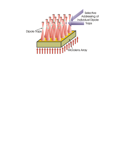

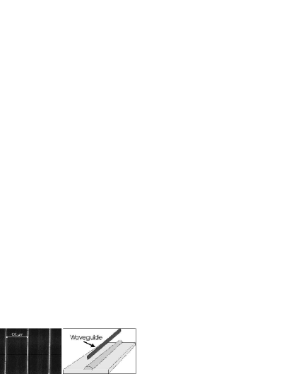
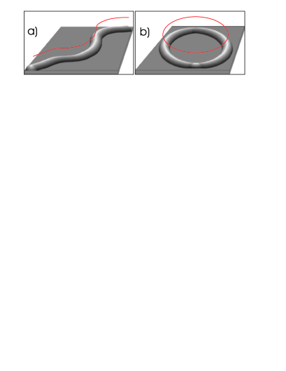
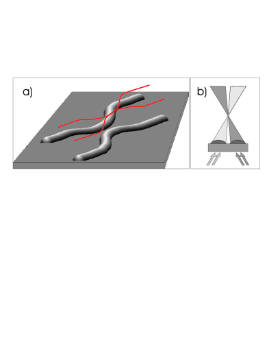
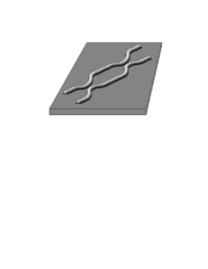

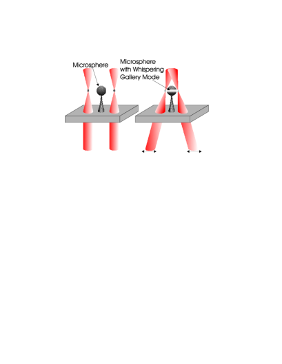
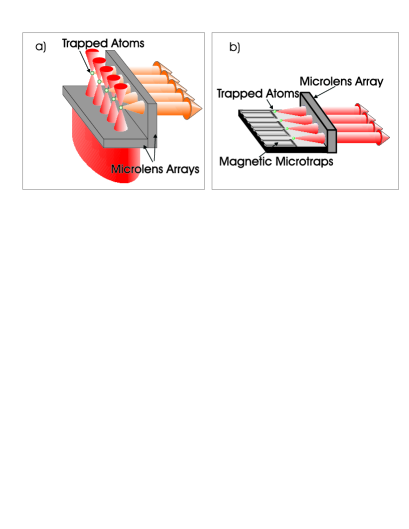
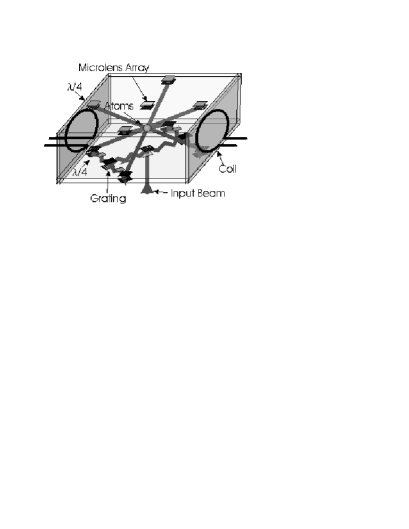
Table I
| Power per | Potential | Vibrational | Ground State | Scattering | |||
| Laser | Lenslet | Depth | Frequency [] | Size [nm] | Rate | ||
| [mW] | [mK ] | [] | |||||
| Diode | |||||||
| (=783nm) | 1 | 6.1 | 22 | 61 | 3800 | ||
| Ti:Sapphire | |||||||
| (=783nm) | 10 | 61 | 13 | 34 | 38000 | ||
| Ti:Sapphire | |||||||
| (=830nm) | 10 | 7.8 | 21 | 57 | 270 | ||
| Nd:YAG | |||||||
| (=1064nm) | 100 | 18 | 17 | 47 | 63 | ||
| (=10,6m) | 1000 | 0.80 | 120 | 270 | 1.3x | ||
Table II
Power Potential Vibrational Ground State Scattering Laser Depth Frequency [] Size [nm] Rate [W] [K ] [] Diode (=783nm) 0.1 59 72 190 37 Ti:Sapphire (=783nm) 1 590 40 110 370 Ti:Sapphire (=830nm) 1 75 67 180 2.6 Nd:YAG (=1064nm) 10 170 53 140 0.6 (=10,6m) 100 77 210 490 1.3x