Atom Chip for Transporting and Merging Magnetically Trapped Atom Clouds
Abstract
We demonstrate an integrated magnetic “atom chip” which transports cold trapped atoms near a surface with very high positioning accuracy. Time-dependent currents in a lithographic conductor pattern create a moving chain of magnetic potential wells; atoms are transported in these wells while remaining confined in all three dimensions. We achieve fluxes up to with a negligible heating rate. An extension of this “atomic conveyor belt” allows the merging of magnetically trapped atom clouds by unification of two Ioffe-Pritchard potentials. Under suitable conditions, the clouds merge without loss of phase space density. We demonstrate this unification process experimentally.
pacs:
32.80.Pj, 03.75.-b, 03.67.Lx, 39.90.+dMiniaturization makes it possible to design tightly confining magnetic atom traps with large field gradients and high field curvature without the need for large currents. With lithographic or other surface-patterning processes complex “atom chips” may be built which combine many traps, waveguides, and other elements in order to realize controllable composite quantum systems [1], as epitomized by the concept of the quantum computer [2].
We are experimenting with lithographically produced planar conducting patterns in an external magnetic bias field as a means to realize microscopic atom manipulation devices. Although lithographic neutral-atom traps have been proposed as early as 1995 [3], the difficulty of loading atoms into such traps has prevented their realization in the past. We have introduced an efficient loading mechanism [4] with the help of a novel mirror-MOT, using a reflecting layer on top of the circuit pattern to realize the laser fields for laser cooling and trapping in close proximity to the surface. In this way, we were able to demonstrate the first lithographic magnetic trap, a quadrupole trap capturing 87Rb atoms. More recently, the same technique has been applied to construct a Ioffe-Pritchard (IP) trap for 7Li atoms [5]. Integrated parallel conductors have also been used to realize atom guides in which atoms are confined in two dimensions and move freely along the third [6, 7]. A different, but related approach was described in [8], where a combination of permanent surface fields and an external bias field produces a series of parallel magnetic tubes, which propagate as the bias field vector rotates. In this experiment, too, the mirror-MOT plays a crucial role in loading the magnetic tubes.
Here we demonstrate an “atomic conveyor belt”, an integrated magnetic device proposed in [4], which transports trapped atoms to very precisely controlled positions near a surface. While the atoms are transported, they remain trapped in all three dimensions, the rms extension of the trap ground state being on the order of 1 m. The speed of displacement can be freely controlled by adjusting the frequency of modulating currents, the device is therefore capable of transporting atoms adiabatically within well-defined quantum states. As we use a thermal atomic cloud in the experiment (temperature in the K range), the adiabaticity of the transport is evidenced by the heating rate, which becomes unmeasurably low for sufficiently slow transport velocity.
An extension of the conveyor belt allows the merging of atom clouds trapped in two adjacent Ioffe-Pritchard (IP) traps. The transfer is complete and, under suitable conditions, occurs without loss of phase space density. We demonstrate this unification process experimentally.
Figure 1 shows the conductor pattern used in the experiment. It is a slightly modified version of the layout proposed in [4]. The width of all relevant conductors is m. In the simplest case, one can create a quasi-2D-Ioffe-Pritchard trap by applying the current to the center wire and superimposing the bias field . The trap center forms at distance from the surface, and if the distance is much smaller than the length of the center wire (5.5 mm in this setup), the longitudinal potential is box-like with a minimum field strength of .
For example, by applying a current A (cf. fig. 1) and a bias field , a very elongated IP trap is formed at a distance of m from the conductor surface. Atom-surface interactions are not expected to be important at such a large distance [9]. For magnetically trapped 87Rb atoms this configuration yields transverse oscillation frequencies of kHz in the trap center, leading to a Lamb-Dicke parameter with respect to the 87Rb D2 line ( is the recoil frequency). An experiment with a potential of this type is described in [10].
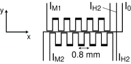
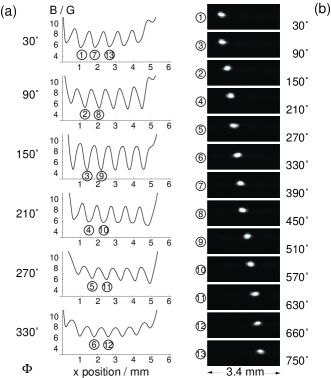
The conveyor potential as displayed in fig. 2(a) is formed starting from such a box-like potential. The field component , which determines the minimum field strength in the transverse (-) plane, is modulated by means of the currents and . Like a bucket chain, the resulting potential consists of a chain of trapping wells that can be continuously displaced along by adjusting the currents and . For the potential in fig. 2(a), a constant current A and the bias field are applied while the modulation currents
| (1) |
create the local minima. As can be seen from figure 2(a), the phase angle determines the position of the minima, so that they can be displaced continuously over the whole length of the conductor pattern. The depth of the individual wells, i. e. the magnetic field difference between the bottom of a well and the saddle point between two adjacent wells, is 2.5 G on average and varies depending on the phase (cf. fig. 2(a)). Transverse (-plane) curvatures are between and near the bottom of the well, leading to oscillation frequencies between 200 Hz and 800 Hz. Longitudinal frequencies are smaller by a factor of 4.
The experimental setup is an improved version of the one described in [4]. Planar gold conductor patterns are formed on an aluminum nitride substrate using a standard microelectronics process known as thin-film hybrid technology (a combination of photolithography and electroplating). The wire thickness (height) is m and lateral dimensions are down to m. Electrical contacts to the substrate are made by gold wire bonding. We load the microtrap from the mirror-MOT ([4], see also [11]), using a reflecting silver layer on top of the circuit pattern to realize the laser fields for laser cooling and trapping in close proximity to the surface. A thin (m) epoxy intermediate layer insulates the circuit pattern from the mirror layer and also fills the gaps between the conductors, leading to a smooth mirror surface. The MOT is loaded from background vapor (total pressure in the mbar range). It typically produces cold atoms within a loading time of 5 s. The atom number is limited by the small diameter and intensity of our trapping beams ( diameter of mm, total power 14 mW). The temperature is K and the peak density in the range after a short optical molasses phase. The initial MOT employs a “macroscopic” quadrupole field created by external coils and is loaded 1 mm away from the surface. By imbalancing the currents in the coils, the cloud is shifted towards the surface (“shifted MOT”); the coils are then switched off and a “microscopic MOT” field with the same orientation is created by switching on and and a bias field along . This combination yields a chain of quadrupole-like potentials. Depending on the position of the shifted MOT, one or several of these small MOTs can be filled with cold atoms. We use both options, depending on the nature of the experiment.
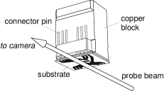
The substrate is mounted upside down in the vacuum cell, so that the atoms are “hanging” below its surface (fig. 3). Thus, time-of-flight (TOF) images can be taken of the atomic cloud released from the magnetic trap to infer its temperature. We observe the atoms by absorptive imaging, using a probe beam along the axis. The images show the horizontal axis (which is the direction of transport) and the vertical axis. The resolution of the imaging system is m. Sensitivity is sufficient to detect 30 atoms per pixel without averaging.
The loading procedure ends with an optical pumping pulse which pumps the atoms to the ground state. After this pulse, the magnetic potential is switched on. Here, the initial potential is the conveyor belt potential (cf. fig. 2) with the parameter , i. e., A, A and . With this phase value, the positions of the well centers coincide with those of the quadrupole fields in the previous “microscopic MOT”, so that atoms are efficiently transferred. We typically obtain trapped clouds with radii m and m, which contain atoms with a peak density of . The lifetime is about s, limited by the background pressure of rubidium and other residual gases.
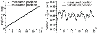
At this point, the conveyor belt is started by varying the phase . Fig. 2(b) shows absorption images of the transport process. (As the imaging is destructive, each image is taken starting from a “fresh” trapped sample.) In this first example, the phase is made to increase linearly with time, with . It should be emphasized, however, that any function of time can be used to control the phase: the atom cloud can be accelerated, or moved at constant speed, or be stopped at any desired position. The positioning accuracy is ultimately limited only by the ground state size, which is m FWHM for the 800 Hz oscillation frequency attained in this potential. The position uncertainty introduced by current fluctuations is orders of magnitude below this value.
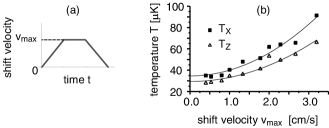
In most applications, it is essential to minimize heating of the trapped cloud during the transport. Leaving aside external mechanisms such as heating by the surface (which is negligible at our atom-surface distance of more than 50 m), transitions may only be induced by the deformation and displacement of the potential wells during the shifting process. The rate of such transitions should decrease to insignificant levels when the speed of displacement is low enough. In our present experiment, where many vibrational states are populated, these transitions translate into heating. We therefore measured the final temperature of the cloud as a function of the maximum shift velocity (fig. 5). For decreasing transport speed, the heating rate decreases, as expected, and becomes unmeasurable within our K accuracy for speeds . In this sense, the transport is adiabatic. When consecutive potential wells are filled with atoms each, the shifting process results in a mean flux of s-1. In a future experiment where single vibrational levels are populated, it will be possible to verify adiabaticity on the quantum mechanical level.
The above data demonstrate the ability to move and position the atom cloud. The conveyor belt can be employed in complex experiments needing precise atom positioning. In cavity QED experiments, for example, it may be used to transport atoms into and out of a zone where they interact with a high-finesse optical resonator, such as a miniature Fabry-Pérot resonator [12, 13] or a silica microsphere [14, 15]. In this way, long and reproducible interaction times and precise positioning of the atomic sample within the quantized resonator field can be achieved. Such a coupling would also enable non-destructive atom detection, as required for quantum computing. Another, more macroscopic application of the conveyor belt would be to transport cold atoms from a production region into a spatially separated interaction region, providing an integrated version of the coil-based magnetic transport device which was recently realized in our laboratory [16].
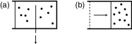
One advantage of the lithographic technique is the ability to combine different potentials very easily. With only one additional wire ( in fig. 1), a stationary IP trap can be formed at the end of the conveyor belt, which adds new options of atom cloud manipulation. The depth of the stationary trap is controlled by current , independently of the conveyor belt movement. Fig. 7(a) shows the resulting potential when (directed along ) is varied according to while all other parameters are controlled as before. (The figure shows only the right part of the potential, cf. fig. 2.) Once per period the stationary trap above continuously unites with the conveyor belt trap arriving from the left. The unification takes place by lowering the barrier between the two traps. At , the two traps are still fully separated. At , their separation has vanished, and at , the united trap has been compressed to the volume originally occupied by the stationary trap. Thus, the process is similar to the classical thermostatistical problem of pulling a septum out of a container, followed by slowly reducing the container’s volume (fig. 6). In particular, if each trap initially contains atoms at equal temperatures and densities, then after one complete cycle, the cloud in the stationary trap should have the same phase space density as before. As it now contains atoms, temperature must have increased during the unification.
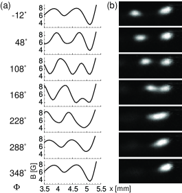
We have implemented this process experimentally by loading two conveyor traps from the MOT and then applying the current modulation described above. Fig. 7 shows the computed potentials (a) as well as absorption images (b) of different stages of the unification process. The potentials have been designed in a way that equally populated traps should merge without loss of phase space density. Due to the difficulty of performing time-of-flight measurements on the two neighbouring clouds, we have not yet been able to measure the phase-space density during this process. Instead one can infer the properties of the unification process by the decrease of phase space density when only one of the two potential wells is initially populated. For this situation, we measure a decrease of per unification, which is close to the decrease of 0.5 expected for the unification of two identical traps one of which is empty.
The unification sequence can also be reversed. In this case, an atom cloud initially localized in the stationary trap is separated into parts during periods. If the separation is done slowly, the process is adiabatic, opening intriguing possibilities for the manipulation of atomic wave packets, including interferometers with trapped atoms. A quantitative study of the unification and separation processes is currently under way.
This work is supported in part by a grant from the European Union (ACQUIRE project, contract no. IST–1999–11055).
REFERENCES
- [1] P. Zoller, Nature 404, 340 (2000).
- [2] See, for example, D. P. DiVincenzo, quant-ph/0002077 (2000).
- [3] J. D. Weinstein and K. G. Libbrecht, Phys. Rev. A 52, 4004 (1995).
- [4] J. Reichel, W. Hänsel, and T. W. Hänsch, Phys. Rev. Lett. 83, 3398 (1999).
- [5] R. Folman et al., Phys. Rev. Lett. 84, 4749 (2000).
- [6] D. Müller et al., Phys. Rev. Lett. 83, 5194 (1999).
- [7] N. H. Dekker et al., Phys. Rev. Lett. 84, 1124 (2000).
- [8] P. Rosenbusch et al., Phys. Rev. A 61, 031404(R) (2000).
- [9] C. Henkel, S. Pötting, and M. Wilkens, Appl. Phys. B 69, 379 (1999).
- [10] J. Reichel, W. Hänsel, P. Hommelhoff, and T. W. Hänsch, Submitted to Appl. Phys. B .
- [11] T. Pfau and J. Mlynek, ”OSA Trends in Optics and Photonics” 7, 33 (1997).
- [12] C. J. Hood et al., Science 287, 1447 (2000).
- [13] P. W. H. Pinkse, T. Fischer, P. Maunz, and G. Rempe, Nature 404, 365 (2000).
- [14] F. Treussart et al., Optics Lett. 19, 1651 (1994).
- [15] D. W. Vernooy et al., Phys. Rev. A 57, R2293 (1998).
- [16] M. Greiner, I. Bloch, T. W. Hänsch, and T. Esslinger, To be published .