A spin-coherent semiconductor photo-detector for quantum communication
Abstract
We describe how quantum information may be transferred from photon polarization to electron spin in a semiconductor device. The transfer of quantum information relies on selection rules for optical transitions, such that two superposed photon polarizations excite two superposed spin states. Entanglement of the electron spin state with the spin state of the remaining hole is prevented by using a single, non-degenerate initial valence band. The degeneracy of the valence band is lifted by the combination of strain and a static magnetic field. We give a detailed description of a semiconductor structure that transfers photon polarization to electron spin coherently, and allows electron spins to be stored and to be made available for quantum information processing.
1 Sun Microsystems Laboratories,
Mountain View, California
2 University of California, Los
Angeles, Electrical Engineering Dept., Los Angeles, California
I Introduction
The development of a quantum computer will likely be preceded by the technology for telecommunication of quantum information. The ability to transfer quantum information from one physical form to another will become valuable . One physical form, a photon in a coherent superposition of polarization states, is particularly suitable for quantum information transport, while another, for example electron spins in a semiconductor host, or the internal states of atoms in a high-Q cavity, may be preferred for quantum information storage and processing. Transfer from one to the other will enable quantum repeaters, quantum networks, and quantum entanglement over long distances. In the short run, such technology, in the form of quantum repeaters, will permit long-distance transmission of quantum cryptographic keys over ordinary fiber.
Several proposals exist to transfer quantum information from photons to atoms trapped in high-Q optical cavities[1, 2, 3]. In this paper we will describe how we may use opto-electronic technology to transfer the quantum information stored in a coherent superposition of photon polarization states to a coherent superposition of electron spin states in a semiconductor. Such electron spin states can have very long dephasing times, or , making them stable against qubit errors. In Silicon at low temperatures, e.g. 1 K, measurements of indicate a lower limit of 0.5 millisecond, limited by the isotopic purity of the material. It is expected that in isotopically pure silicon, in which all nuclei have spin zero, the will even be longer since the most important decoherence mechanism, spin-diffusion will be eliminated. Similarly long times are expected to occur in low-temperature Germanium. Such long times allow for extensive quantum information processing and error correction or temporary storage of the information.
For coherent optical detection of quantum states however, we will need a device with extremely high quantum efficiency, which can only be achieved in the direct-bandgap III-V materials. In III-V semiconductors, all nuclei have a net spin, and the electron times are significantly shorter. However, they are still long enough, on the order of 100 nanoseconds[4], that quantum logic operations may be performed, particularly the teleportation algorithm.
II Quantum State Coherent Photodetector
It is well known that polarized electrons can be created by illuminating GaAs with circularly polarized light. The valence band of GaAs has angular momentum . Combined with the spin of the electron , this gives rise to four states. The conduction band wavefunction is an -wave, with . A righthanded circularly () polarized photon, only couples the valence state with to the conduction band state. Thus, upon irradiation with righthanded circularly polarized light, only electrons with spin down are created. Similarly, left handed circularly polarized light only creates spin up electrons. This polarization sensitivity is in fact used in photocathodes for spin polarized high-energy electron accelerators[5].
However, this system is not suited for transferring quantum information, encoded in an arbitrary superposition of polarization states, from a photon to an electron. Consider a photon qubit, in a superposition of circular polarization states:
| (1) |
Since the two polarizations couple two different valence band states to the respective conduction band states, they will also create two different hole states. The electron thus created will be entangled with the hole, with the final state of the electron-hole pair given by:
| (3) | |||||
This is an undesirable state, since in order to preserve the quantum information, or process it, we would have to maintain coherence for both the electron and the hole. Most likely the hole will interact with the rest of the system and the superposition will collapse into one of the two eigenstates in Eqn (3) of the system, and destroy the quantum information.
To avoid this problem, we have to make sure that no information is left behind in the hole state. Therefore, the two conduction band polarizations have to be accessible from a single valence band state. The two orthogonal photon polarizations should couple the single valence state to both conduction band electron spin states. Here we describe two important configurations in which this is possible. Both rely on the capability to create a completely non-degenerate topmost valence band state. This valence band can be optically selected by using photons of an energy sufficient to couple only that state to the conduction band. The other valence bands are energetically too far removed from the conduction band and can not be excited.
The degeneracy between heavy hole states () and light hole states () is lifted if the material is placed under strain, by growing heterostructures of materials with different lattice constants, or by size quantization in a quantum well. Generally, in compressively strained materials, the heavy hole band is the topmost band, while materials under significant tensile strain have the light hole band on top. The growth direction thus establishes a quantization axis. Finally, the remaining degeneracy between the spin up and spin down components of both bands is lifted by a static magnetic field. This magnetic field is chosen small enough, so that the Zeeman perturbation is small compared to the strain splitting.
A Case A: Magnetic Field Normal to Sample Surface
In a sufficiently tensile strained semiconductor, the topmost valence band is the light hole band. By applying a magnetic field parallel to the growth direction the band is split into its two Zeeman sublevels. The energy splitting between these two states is given by
| (4) |
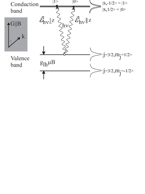
where is the Landé -factor of the valence band. The conduction band spin levels are also split by the magnetic field, but the Zeeman energy can be very different from that of the conduction band. The conduction band -factor, can have a much smaller value than , as will be discussed below. Accordingly, we can have the situation in which the incident light has a bandwidth larger than the conduction band Zeeman energy, but smaller than the valence band Zeeman energy. Thus, we have a well defined, single initial valence-band state, while the two conduction band spin states are practically degenerate. The resulting level configuration is given in Fig (1). The uppermost valence level, with , forms the single valence band state from which both conduction band levels are accessed. We can see how this is possible by expanding the in the LS basis:
| (5) |
The photon only interacts with the spatial part of the wavefunction. Photons polarized along the quantization axis, i.e. in the z-direction, do not change the number, and thus only couple the part of the wavefunction to the conduction band, which is exclusively . Alternatively, photons polarized perpendicular to the quantization axis change the magnetic quantum number by 1, and thus exclusively interact with the part of the wavefunction, by coupling the valence state to the conduction state.

/noindent Thus each polarization component exclusively excites one electron spin component, while the hole state remains common to both. Explicitly, if we have a photon qubit in an arbitrary superposition of the two linear polarization states and :
| (6) |
it will excite an electron-hole pair with a wavefunction
| (8) | |||||
| (10) | |||||
As is obvious from Eqn (10), the state of the hole can be factored out of the wavefunction of the system and no information is carried away by the hole. The electron and hole are disentangled. Furthermore, the quantum information originally stored in the photon, is completely transferred to the electron spin.
B Case B: Magnetic Field Parallel to Sample Surface
In Part A, the case of magnetic field normal to the sample surface was treated. As shown in Eqn. 5, the weighting amplitude for optical absorption into up versus down spin differs by . This can be compensated by using an off-center wavelength for the optical transition, but it can also be eliminated by magnetic field parallel to the sample surface as follows. With magnetic field parallel to the sample surface, a new quantization axis is created, in which the regular quantum eigenstates of the normal axis case are equally super-posed.
For case A, the heavy hole valence band was not useful, since the heavy hole states coupled purely to electron states, and were unable to create the required quantum mechanical superposition. With the magnetic field parallel to the surface, a new quantization axis is created, that creates an equal superposition but suffers from another problem. The component of the heavy hole -tensor parallel to the surface vanishes for heavy holes. Thus the requirement for an optically resolvable valence band Zeeman splitting cannot be achieved for heavy holes. Now in case B, as previously in case A, heavy holes are not useful for creating superpositions of quantum states. However, an equal superposition can be created in case B for a light hole valence band. In this case the band will be split into two levels and :
| (11) | |||||
| (12) |
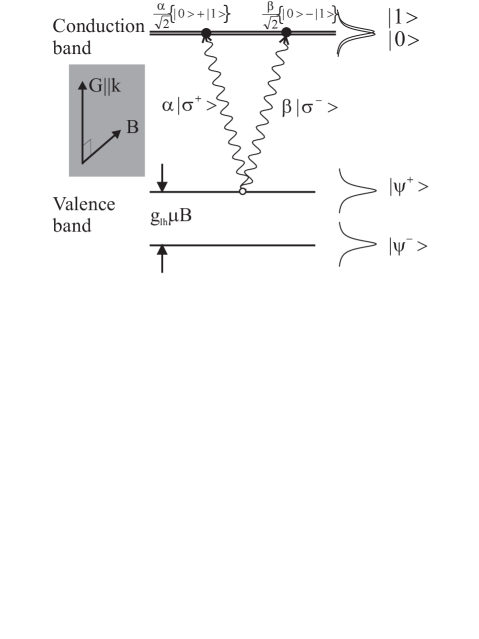
Using as the initial state, it is possible to couple to the conduction band state by exciting a conduction band electron with a righthanded circularly polarized photon (). At the same time, a lefthanded circularly polarized photon will excite the conduction band state. Again, the conduction band -factor is much smaller than the valence band -factor, so that both conduction band spin states are energetically accessible. Note that the quantization axis for the photons, or the -vector, coincides with the strain direction in the semiconductor, and is perpendicular to the static magnetic field . Again, the non-degenerate valence band state is the same for both cases, and no quantum information is retained in the hole. One major difference with respect to case A is that the excited conduction band electron state is not an eigenstate of the system. This is due to the magnetic field being perpendicular to the quantization axis. Therefore the spin eigenstates of the conduction band electron are:
| (13) | |||
| (14) |
After excitation of a pure or a pure the conduction band electron spin will precess around this magnetic field. The precession time is given by . Let us consider the excitation of the system with a photon carrying quantum information:
| (15) |
The system, initially in is excited to a superposition:
| (16) | |||||
| (17) |

As long as the coherence is preserved, i.e. within a , the precession of the electron spin does not destroy the quantum information present in the superposition of the two spin states. A well-synchronized Hadamard transform will take the system from a superposition of precessing states to a corresponding superposition of the two eigenstates and . The quantum information has again been successfully transferred to the spin of the electron, without any entanglement with the hole that is left behind.
C g-factors of valence- and conduction band
Essential to the proposed detection mechanisms is that both Zeeman levels of the conduction band electron are accessible within the bandwidth of the exciting photon, while the two Zeeman levels in the valence band are spectrally resolved. Therefore it is crucial to find, or rather engineer, a material in which the g-factor of the conduction band electron is significantly smaller than the g-factor of the valence band hole. Fortunately, in III-V semiconductors, the valence band states have rather large spin-orbit coupling which allows engineering of the g-factor. An example is the InAs/GaAs quantum well as described in ref[6]. In this system, the conduction band electron g-factor is , while the light-hole -factor can as large as . Such a large difference in -factor allows the valence bands to be energetically resolved, while, at the same magnetic field, the conduction band spin states are spectrally overlapping.
III Spin Coherent Photo Detector and Emitter
A Detector

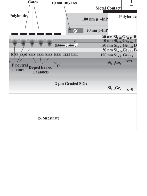
In Fig (3) a schematic illustration of the proposed spin coherent receiver is given. In the device we combine silicon and III-V technology. The materials are joined by the technique of wafer fusion. This is a commercial process, and it allows us to combine the high optical efficiency of III-V semiconductors with the extremely long lifetimes that electron spins enjoy in a type IV semiconductor host, particularly silicon. The electron is generated in a 10-nm thick InGaAs quantum well, which is embedded in p-doped InP. The quantum well is optically thin, so that the absorption needs to be enhanced by an optically resonant cavity[7].
After generation, the hole is swept to ground through a heavily doped -InP layer. The hole carries no quantum information whatsoever, i.e. is not entangled with the spin states of the conduction band electron. The electron is transported through the wafer-fused layer into the storage and processing part of the spin-coherent receiver by electrostatic fields. Such transport can be performed while retaining coherence to a remarkably high degree, as was recently demonstrated in an experiment by Awschalom et al[4]. The storage and processing part of the detector is in fact a small quantum processor. This indicates how the first application of small quantum computers may in fact be to boost the throughput of quantum communication channels. The logic gates are in the SiGe heterostructure, which has been described in detail elsewhere[8]. The layers with a Si0.09Ge0.91 composition, labeled B, are barrier layers with a relatively high bandgap, to confine the electron in the region of interest. Between these layers, the electron is bound to a 31P+ ion, which is implanted underneath an electric gate. There the electron remains bound, but the information stored in its spin states can be swapped further into the computer, through spin-exchange, or two-qubit, operations with neighboring electrons bound to identical 31P dopant ions, also placed under gates. The required control is obtained by applying gate voltages, and by the fact that the -factor of the bound electron is modulated between the two barrier (B) layers. In the Ge-rich Si0.04Ge0.96-layer, also called T for tuning layer, the -factor is Ge-like, and has a value of in the direction . In the Si-rich Si0.22Ge0.78, or D(onor), layer, the -factor is Si-like, with . By modulating the gate voltage, the electron wave-function is pulled more or less toward the electrode through the Stark-effect. This in turn modulates the -factor. In the presence of a constant background microwave radiation field, the electron spin can thus be pulled in and out of resonance. This allows single-qubit interactions. The two-qubit interaction is achieved through the application of positive gate voltages to adjacent electrodes. Both electrons are pulled away from their ions, and the reduced Coulomb interaction allows an increased Bohr radius. This causes an increased interaction between the neighboring electrons, and turns on the exchange interaction. As shown by Loss et al[9], this exchange interaction can be used to perform swap, and controlled NOT operations between qubits. These one- and two-qubit interactions together form a universal set of quantum gates, so that any unitary transformation can be performed on the quantum information stored in the bound electron spins, including error correction and quantum information processing.
B Photon Emitter
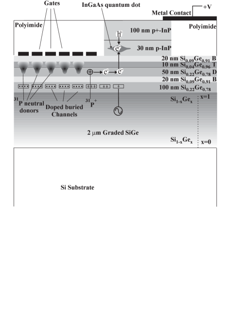
After error correction, teleportation, or other quantum information processing steps, we want to re-emit the stored quantum information as a photon. This is possible by running the reverse of the detection process. The electron needs to be recombined with a hole, where only one type of hole is allowed to interact with the electron. Since we chose our holes to be in the top of the valence band, this will not be a problem since they will naturally be the abundant ones. The photon emitter therefore looks very similar to the photo-receiver, as shown in Fig (4).
The information that needs to be transmitted is first swapped to the electron bound to the rightmost 31P dopant ion. This electron is pulled off the ion by applying a relatively strong pulse to the gate electrode, and is electrostatically transported to the InGaAs quantum dot. A hole is injected into the dot as well so that electron-hole recombination can take place. Upon recombination the quantum information is transferred to the emitted photon, following the same selection rules that governed the transfer in absorption.

The quantum dot is a slight modification with respect to the quantum well in the receiver and ensures that the electron wavefunction is confined in space and is not free to move around in the time before a photon is emitted. In the receiver, the electron is swept away from the III-V material as soon as it is generated. In the emitter however, we have to wait for the electron to interact with the single injected hole, which may take several nanoseconds. A free electron would sample many different spins in such a lifetime, and decohere rapidly. By confining the electron to a dot, such movement is precluded. The quantum dot needs only to be small enough so that the confinement energy of the quantum dot is larger than , and so that the charging energy satisfies as well[10]. Furthermore, to assure a long enough capture time, the tunneling resistance for electrons flowing into the quantum dot should be . All these requirements can be met simultaneously even with a moderate sized quantum dot, patterned by e-beam lithography.
One complication in the emitter is that, whereas the incident photon in the detector had a definite -vector, the emitted photon, can be emitted isotropically. Not all directions obey the same selection rules however, since the relative orientation of the spin-quantization axis and the photon -vector varies with the emission direction. Therefore it may be necessary to introduce complex quarter-wave plates or phase plates to compensate for the photon polarization differences in different directions in the optical collection system.
Summarizing, we have indicated how optical selection rules may be used to transfer quantum information from one physical form to another, i.e. from photon polarization to electron spin and vice versa. A key ingredient is the removal of all degeneracies from the initial valence band state, to prevent entanglement of the conduction band electron spin state and the remaining hole. We have described a detector and emitter device combining a optically highly efficient III-V component with a type-IV storage and processing component, in which the electron spins have exceedingly long lifetimes, based on such selection rules. Such a device may become an indispensable component in quantum communication technology by boosting the data rate of existing channels, and by enabling the long-distance transfer of fully quantum states.
The authors would like to acknowledge fruitful discussions with Tal Mor, Oscar Boykin, Vwani Roychowdhury and Ivair Gontijo. This work was sponsored by the Defense Advanced Research Project Agency (Grant No. DAAD19-00-1-0172) . The content of this paper does not necessarily reflect the position or policy of the Government, and no official endorsement should be inferred.
REFERENCES
- [1] J. I. Cirac, P. Zoller, H. J. Kimble, and H. Mabuchi, Phys. Rev. Lett. 78, 3221 (1997).
- [2] T. Pellizari, Phys. Rev. Lett. 79, 5242 (1997).
- [3] S. J. van Enk, J. I. Cirac, and P. Zoller, Phys. Rev. Lett. 78, 4293 (1997).
- [4] D. D. Awschalom and J. M. Kikkawa, Phys. Today 52, 33 (1999).
- [5] H. M. Al-Khateeb, B. G. Birdsey, T. C. Bowen, A. S. Green, M. E. Johnston, and T. J. Gay, Rev. Sci. Instrum. 70, 3882 (1999).
- [6] A. A. Sirenko, T. Ruf, N. N. Ledentsov, A. Yu. Egorov, P. S. Kop’ev, P. S. Ustinov, and A. E. Zukov, Sol. State Comm. 97, 169 (1996).
- [7] J. D. Schaub, R. Li, C. L. Schow, J. C. Campbell, G. W. Neudeck, and J. Denton, IEEE Phot. Tech. Lett. 11, 1647 (1999).
- [8] R. B. Vrijen, E. Yablonovitch, K. Wang, H. W. Jiang, A. Balandin, V. Roychowdhury, T. Mor, and D. DiVincenzo, Phys. Rev. A 62, 12306-1/10 (2000).
- [9] D. Loss and D. P. DiVincenzo, Phys. Rev. A 57, 120 (1998).
- [10] J. Kim, O. Benson, H. Kan, and Y. Yamamoto, Nature 397, 500 (1999).