A fast programmable trigger for isolated cluster counting in the BELLE experiment
Abstract
We have developed a fast programmable trigger processor board based on a field programmable gate array and a complex programmable logic device for use in the BELLE experiment. The trigger board accommodates 144 ECL input signals, 2 NIM input signals, 24 ECL output signals, and the VME bus specification. An asynchronous trigger logic for counting isolated clusters is used. We have obtained trigger latency of 50 ns with a full access to input and output signals via a VME interface. The trigger logic can be modified at any time depending on the experimental conditions.
keywords:
Trigger; FPGA; CPLD; VMEPACS:
07.05.Hd, 07.50.Qx, 07.50.Ek1 Introduction
Fast, complex, general-purpose trigger systems are required for modern particle physics experiments. Although custom-made CMOS gate arrays are used for extremely fast applications such as first-level triggers ( 25 ns) for LHC experiments[1], field programmable gate arrays (FPGAs) are an attractive option for environments that require a less demanding speed ( 100 ns) but a more flexible trigger logic implementation. The logic of FPGA-based trigger systems can be readily changed as the nature of signal and background conditions vary. Such trigger systems are flexible and can be adapted to many different applications. Commercial products that have these functionalities exist (for example, the Lecroy 2366 Universal Logic Module, Lecroy Co.) and can be used for implementing rather simple trigger logic. In the case of the calorimeter trigger for the BELLE experiment, the number of channels, data transfer rates, and the complexity of the trigger logic preclude the use of commericially available devices. We developed a 9U VME[2] module that accommodates more than a hundred ECL signals for the triggering purpose. The resulting board is a general purpose asynchronous programmable trigger board that satisfies VME specifications.
2 Trigger requirements for the BELLE Experiment
The BELLE experiment[3] at KEK in Japan, is designed to exloit the physics potential of KEKB, a high luminosity, asymmetric collider operating at a cm energy (10.55 GeV) corresponding to the resonance. In particular, BELLE is designed to test the Kobayashi-Maskawa mechanism for CP violation in B meson sector. The KEKB design luminosity is 1 cm-2s-1 with a bunch crossing rate of 2 ns. The BELLE detector consists of seven subsystems; a silicon vertex detector (SVD), a central drift chamber (CDC), an aerogel Cherenkov counter (ACC), an array of trigger and time of flight scintillation counters (TOF/TSC), an electro-magnetic calorimeter (ECL), and muon detectors (KLM) and extreme forward calorimeters (EFC). A 1.5 Tesla axial magnetic field is produced by a superconducting solenoid located outside of the ECL. The KLM is outside of the solenoid and provides a return yoke for the detector’s magnetic field. The BELLE trigger system requires logic with a level of sophistication that can distinguish and select desired events from a large number of background processes that may change depending on the conditions of the KEKB storage ring system. Figure 1 shows a schematic view of the BELLE trigger system. As shown in Fig. 1, the trigger information from individual detector components is formed in parallel and combined in one final stage. This scheme facilitates the formation of redundant triggers that rely either only on information from the calorimeter or from the tracking systems. The final event trigger time is determined by requiring a coincidence between the beam-crossing RF signal and the output of the final trigger decision logic. The timing and width of the subsystem trigger signals are adjusted so that their outputs always cover the beam-crossing at a well defined fixed delay of 2.2 s from the actual event crossing.
The ECL is a highly segmented array of 9000 CsI(Tl) crystals with silicon photodiode readout installed inside the coil of the solenoid magnet. Preamplifier outputs from each crystal are added in summing modules located just outside of the BELLE detector and then split into two streams with two different shaping times (1 s and 200 ns): the slower one for the total energy measurement and the faster one for the trigger. For the trigger, signals from a group of crystals are summed to form a trigger cell (TC), discriminated, digitized (as differential ECL logic signals), and fed into five Cluster Counting Modules (CCMs) that count the number of isolated clusters in the calorimeter. In total, the ECL has 512 trigger cells: 432 in the barrel region and 80 in the endcaps. The trigger latency of the CCM trigger board is 150 ns. Each module accepts 132 inputs and outputs 16 logic signals. (The actual board can accommodate a maximum of 144 inputs and provide as many as 24 output signals; for BELLE we have chosen to use 132 input and 16 output lines per board).
Given the complexity discussed above and the required flexibility, we chose to use a complex FPGA to apply the isolated clustering algorithm and a CPLD device in order to match the VME bus specifications. For the FPGA, we use an XC5215-PG299 chip that has 484 configurable logical blocks (CLBs), and for the CPLD, an XC95216-5PQ160, which provides 4,800 usable gates. Once the CPLD is loaded, it permanently holds all of the VME bus specification logic. In contrast, the trigger logic contained in the FPGA is lost during a power down, and must be reconfigured during start-up, either from an on-board PROM or from a computer (VME master module) through VME bus. This takes a few milliseconds. In the following we describe in some detail the trigger logic design of the CCM board and how we achieve our performance requirements.
3 Logic Design
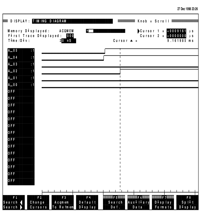
We used XACTTM software provided by Xilinx[4] to design, debug and simulate our logic. The trigger processor board accepts the differential ECL logic signals from the calorimeter trigger cells. There are many possible strategies for finding and counting the number of isolated clusters (ICN) among the calorimeter trigger cells. But, since the trigger decision has to be made within a limited time period, a simple algorithm is desirable. We devised simple logic that counts only one cluster from a group of connected clusters. For the case of a number of connected clusters, we count only the upper most cluster in the right most column among them. This is demonstrated for a 3 3 trigger cell array in Fig. 2. Here, the trigger cell under the counting operation is numbered as “0”. If the cell “0” satisfies the logic diagram shown in Fig. 2, it is considered to be a single isolated cluster. We have applied this simple logic to the output of GEANT-based[5] full Monte Carlo simulation of various decay modes as well as Bhabha scattering events and compared the perfect cluster number and the cluster number returned by the above logic. The results are summarized in Table 1. In all the cases, the discrepancies between the perfect cluster counting and the isolated cluster counting logic are below the 1 % level; despite its simplicity, the counting logic works exceptionally well. This simple clustering logic is applied to over 132 input signals and the number of isolated clusters are then tallied. In addition to the cluster counting logic, we also delay the 132 input and 16 output signals and register them in a set of FIFO RAMs (the pattern register) located on the board. The signals are delayed (in order for them to be correctly phased) by approximately 800 ns by means of an 8 MHz delay pulse and stored in FIFO RAMs at the trigger decision. The delay time can be easily changed by modifying the logic. The pattern register allows a continuous monitoring of the operation of the CCM module. The recorded cluster and ICN bits are read out through the VME bus independently of the ICN counting system. The FPGA counts the number of clusters asynchronously and the simulated timing diagram in Fig. 3 indicates that the time needed for the ICN counting is 47 ns.
In order to satisfy the complete VME bus specification, a set of logical blocks (Address Decoder, Interrupter, Control Logic, Configuration Control Logic, CSR, and FIFO RAM Control) are developed and downloaded into the CPLD. The logical blocks are designed as a VME A24/D32 slave interface. Comparators are used to decode addresses being probed by the master module. Status bits are implemented in order to check the status of the configuration completion of FPGA chip and triggering process itself. Control bits are implemented to stop the output of the triggering signal, to start the output of the triggering signal, to enable the reconfiguration of the FPGA chip via a PROM or the VME bus, and to control the FIFO RAM that serves as the pattern register. All the functionalities were tested extensively during the development phase and completely debugged before they were implemented in the experiment.
4 Hardware Implementation
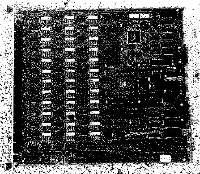
The CCM module houses the main FPGA chip for the ICN counting, the CPLD chip for implementing the VME bus specifications, ECL-TTL and NIM-TTL converters, the PROM holding the FPGA configuration, and the FIFO RAM pattern register. A schematic diagram and an assembled board are shown in Figs. 4 and 5, respectively. The printed circuit board is a VME 9U size four-layer board. All connectors, switches, components, and downloading circuitry are mounted on one side of the board. The logic signals to and from the FPGA are TTL CMOS, and are interfaced with the differential ECL logic signals to the rest of the trigger and data acquisition system. Standard 10124 (10125) chips with 390 pull down resisters (56 2 termination resisters) are used to convert TTL to ECL (ECL to TTL). The input polarity is such that a positive ECL edge produces a negative TTL edge at the FPGA input. Also on-board are several discrete-component, NIM-TTL converters that interface with two external NIM control signals: the master trigger signal (MTG) and the external clock. Three 7202 CMOS asynchronous FIFO chips ( 3 1024 Bytes ) provide the pattern register. The actual registration for one event includes 132 inputs, 16 outputs, 8 reserved bits, 10 memory address bits, and 2 unsed bits; a total of 146 bits are registered in the three FIFO chips.
Programs for the FPGA chip can be downloaded from an on-board PROM (Master Serial Mode) or via the VME bus (Peripheral Asynchronous Mode). We use an XC17256D Serial Configuration PROM and the clustering logic is downloaded by a PROM writer that is controlled by a personal computer. The choice of the VME master module is the FORCE[6] SUN5V, a 6U VME bus CPU board that has a 110 MHz microSPARC-II processor running Solaris 2.5.1. Accessing the CCM from the VME master module is simply done by mapping the device (in our case, the CCM) into the memory of the master module. From there, the clustering logic can also be loaded into the FPGA chip. All of the control software was developed in this master module with GNU[7] gcc and g++ compilers. An object-oriented graphical user interface based on the ROOT[8] framework was also developed. Resetting the module, downloading the logic to FPGA from the PROM or the VME bus, and the FIFO reading are all implemented in the graphical user interface. Programs for the CPLD chip are downloaded through an on-board connector from the parallel port of a personal computer and it enables the downloading of the CPLD program whenever necessary.
The base address of the board is set by a 8-pin dip switch on board. A hardware reset switch that resets the FPGA, the CPLD, and the FIFO RAMs is provided on the front panel. There are four LEDs indicating power on/off, MTG in, and two configuration of FPGA completion (LDC and SX1). Two fuses (250V 2A) and four capacitors (100 F) are on 5 V lines for the protection purpose.
The trigger board has been fully tested and the results have been compared with software simulations. Test results are shown in Fig. 6, where a cluster-counting time of approximately 50 ns is found, which is in good agreement with the 47 ns time predicted by the simulation.
5 Performance with e+e- collisions
The BELLE detector started taking e+e- collision data with all subsystems, the data acquisition systems, and accompanying trigger modules operational in early June of 1999. Six CCM modules installed in the electronics hut counted isolated clusters from the e+e- collision in the calorimeter. Five CCM modules were used to count isolated clusters from the five sections of the calorimeter; the sixth module collected and summed the outputs from the other five. The flexibility inherent in the design of the board allowed the use some of the input and ouput channels of the sixth module to generate triggers for Bhabha events as well as calorimeter timing signals.
In a 100K event sample of actual triggers, we found a nearly perfect correspondence between the numbers of isolated clusters provided by the trigger logic and those inferred from TDC hit patterns that are available at the offline analysis stage. Figure 7(a) shows the correlation between the number of isolated clusters from TDC hit patterns and ICN numbers from CCM modules. As is shown here, there are few cases that ICN numbers from CCM modules are smaller than numbers from TDC hit patterns. Figure. 7 (b) shows the mismatch rate between the TDC-based and-CCM based cluster numbers as a function of the TDC-based cluster numbers. For more than 99.8 % of the cases, the two numbers are identical. We attribute the small level of inconsistency to the limitations of the clustering counting logic (see section 3) and the infrequent occurence of timing offset on the input signals.
6 Conclusions
We have developed a fast trigger processor board utilizing FPGA and CPLD technology. It accommodates 144 ECL input signals and provides 24 ECL output signals. It functions as a 9U VME module that enables the loading of revised trigger logic and the online resetting of the module. In addition, a pattern register on the board contains all of the input/output ECL signals that were used in a process. The isolated clustering logic is measured to have a time latency of 50 ns, in good agreement with the prediction of the simulation. Sufficient hardware and software flexibility has been incorporated into the module to make it well suited for dealing with a variety of experimental conditions.
References
- [1] Annu. Rev. Nucl. Sci. 44 609 (1994).
- [2] VME bus International Trade Association, VMEbus Specification Manual ANSI/IEEE STD 1014-1987 (1987).
- [3] The BELLE Collaboration, Technical Design Report, KEK report 95-1 (1995).
- [4] Xilinx Inc., San Jose, CA, USA.
- [5] GEANT, Detector Description and Simulation Tool, CERN program library long writeup W5013.
- [6] Force Computers Inc. 2001 Logic Drive, San Jose, CA, USA.
- [7] Free Software Foundation, Inc., 59 Temple Place - Suite 330, Boston, MA 02111, USA.
- [8] ROOT - An Object Oriented Data Analysis Framework, Proceedings AIHENP’96 Workshop, Lausanne, Sep. 1996, Nucl. Inst. & Meth. in Phys. Res. A 389 (1997) 81-86. See also http://root.cern.ch/.
| ICN(logic)-ICN(perfect) | 0 | 1 | 2 |
|---|---|---|---|
| Bhabha | 100 | 0 | 0 |
| 99.15 | 0.85 | 0.00 | |
| 98.55 | 1.45 | 0.00 | |
| 99.15 | 0.85 | 0.00 | |
| 98.95 | 1.05 | 0.00 | |
| 98.95 | 1.05 | 0.00 | |
| 99.15 | 0.80 | 0.05 | |
| 99.15 | 0.85 | 0.00 |