Substrate-based atom waveguide using guided two-color evanescent light fields
Abstract
We propose a dipole-force linear waveguide which confines neutral atoms up to above a microfabricated single-mode dielectric optical guide. The optical guide carries far blue-detuned light in the horizontally-polarized TE mode and far red-detuned light in the vertically-polarized TM mode, with both modes close to optical cut-off. A trapping minimum in the transverse plane is formed above the optical guide due to the differing evanescent decay lengths of the two modes. This design allows manufacture of mechanically stable atom-optical elements on a substrate. We calculate the full vector bound modes for an arbitrary guide shape using two-dimensional non-uniform finite elements in the frequency-domain, allowing us to optimize atom waveguide properties. We find that a rectangular optical guide of 0.8 m by 0.2 m carrying 6 mW of total laser power (detuning 15 nm about the D2 line) gives a trap depth of 200 K for cesium atoms (), transverse oscillation frequencies of kHz and kHz, collection area m2 and coherence time of 9 ms. We discuss the effects of non-zero , the D1 line, surface interactions, heating rate, the substrate refractive index, and the limits on waveguide bending radius.
pacs:
03.75.Be, 32.80.PjThere has been much recent progress in the trapping and cooling of neutral atoms, opening up new areas of ultra-low energy and matter-wave physics [4]. Waveguides for such atoms are of great interest for atom optics, atom interferometery, and atom lithography. Multimode atom waveguides act as incoherent atom pipes that could trap atoms, transport them along complicated paths or between different environments, or deliver highly localized atom beams to a surface. Single-mode waveguides (or multimode guides populated only by atoms in the transverse ground-state) could be used for coherent atom optics and interferometry [12, 10], as well as a tool for one-dimensional physics such as boson-fermion duality [9, 25, 26] and low-dimensional Bose-Einstein condensation effects [27].
The optical dipole-force has long been used to trap and manipulate atoms [4] as well as dielectric particles [6]. The available intensity of lasers has allowed a multitude of such atom traps in the far-detuned regime, giving very low decoherence and heating rates, and storage times on the order of seconds [5].
Evanescent light waves have been popular in many atom mirrors, traps and guides [13, 14] since they can provide potentials with high spatial gradients (decay lengths where is the optical wavelength), and use rigid dielectric structures (prisms, fibers) to define the potential shape. For example, there has been a series of repulsive (blue-detuned) evanescent-wave (EW) traps which rely on gravity to provide the counteracting force [15] and recent experiments have shown that hollow optical fibers can guide atoms confined within the hollow core using a repulsive evanescent field guided by the fiber [22, 23].
The idea of using an EW to provide both attractive and repulsive forces is due to Ovchinnikov et al. [16], who proposed the use of two colors (i.e. red and blue detunings) and differing evanescent decay lengths to achieve a trap with the potential minimum a distance from a prism surface. Until now, this design has been restricted to planar traps (weak confinement in the other two dimensions).
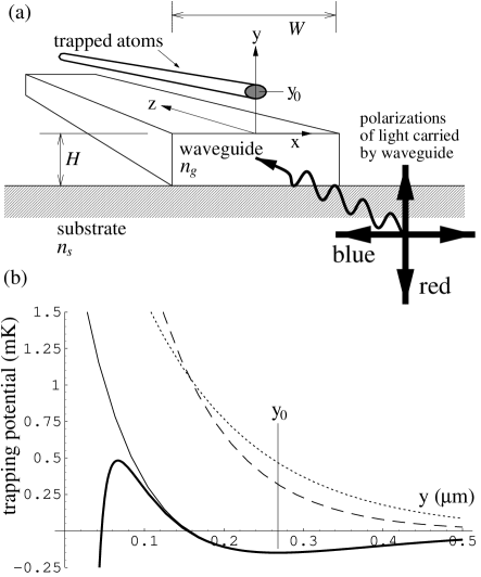
In this paper we discuss a two-color trap based on the EW fields above a single-mode, submicron optical ‘channel’ waveguide. The trap provides tight confinement in two dimensions and allows free de Broglie wave propagation in the third, forming an atomic waveguide that could transport atoms a between and above the optical guide surface. Our proposal is to utilize the differing vertical evanescent decay lengths of the two polarizations carried in the single-mode optical guide (see Figure 1). The physical origin of this decay length difference is the fact that the TM mode is closer to optical cut-off than the TE mode at the same frequency.
Our proposal is reminiscent of some existing resonant enhancement schemes for EW mirrors (demonstrated with surface plasmons [17] and dielectric waveguides [18]) but with a radical change from a planar geometry to a linear, the mechanism for exciting the guide, and the simultaneous guiding of a second frequency of opposite detuning. It also shares the feature of two guided colors with an atom trap proposal using microsphere whispering-gallery modes[19].
Our design has many desirable experimental features: 1) very little optical power is required to obtain large trapping intensities since the optical bound mode has very small cross sectional area (), 2) the optical field is non-divergent, so can be maintained over distances orders of magnitude further than diffraction-limited propagation in free space allows, 3) the trapping potential is well-known, mechanically stable, and insensitive to experimental parameters other than the optical powers, since it is defined by single-mode intensity distributions fixed relative to a substrate, 4) fabrication of arrays of closely spaced atom waveguides is possible[34], for parallel lithography or measurement, creating “on-chip” integrated atom-optical elements, 5) the atoms are exposed providing additional optical and physical access (a feature not shared with hollow-fiber designs), and 6) the velocity of the atoms along the direction of the waveguide could be controlled by standing waves in the light carried by the optical guide [24].
Compared to a Zeeman-effect magnetic trap for neutral atoms, far-detuned optical dipole-force traps can have comparable trapping times, but typically an order of magnitude less depth and transverse mode spacings than recent magnetic traps [7, 8, 9]. However, in microfabricated applications the stray magnetic fields decay as a power law with distance, whereas evanescent light fields decay exponentially (ignoring for now any scattering into free space caused by optical defects). We believe this could give guided optical traps a distinct advantage in terms of achievable density of independent atom-optical elements on a single substrate.
Also, optical traps have the advantage that there is no significant loss mechanism which can remove atoms from the trap (assuming the thermal energy is much less than the trap depth): spontaneous events cause a small heating rate, and non-adiabatic changes in can change the optical potential but not the fact that the atom remains trapped. This is to be contrasted with a non-adiabatic spin-flip event in a magnetic trap, which results in loss of the atom. This makes optical waveguides particularly attractive for incoherent transport, when the loss of coherence due to the spontaneous events is unimportant. Finally, optical manipulation has the advantage over magnetic manipulation in terms of high possible switching speeds.
This paper is organized as follows. In Section I we describe the dipole potential, the exponential approximation for the EW fields, and the mechanism for the difference in decay length. We show how we optimized the optical guide dimensions, in the case of a rectangular guide on a substrate of unity refractive index (for ), and discuss some design objectives and implementation issues. In Section II we give simulated results for cesium atoms: trap depth, coherence time, transverse mode spacing and Q factor, and spontaneous heating rate. We also show how depth and coherence time are generally limited by only two parameters (the detuning and the normalized decay length difference). We study both the case of a substrate refractive index of unity, and in Section II C the more realistic index of 1.32. We describe the numerical electromagnetic finite element technique in Section III, including the accuracy achieved. Section IV is an investigation of two potential causes of loss or decoherence of atoms, namely interactions with the dielectric surface and bending of the waveguide. Finally in Section V we conclude and give some future prospects for this proposal.
I Trap Concept
A Theory of the light potential
An atom in a near-resonant light field of frequency experiences both a conservative force (due to stimulated photon exchange) and a dissipative force (due to spontaneous photon emission)[20, 21]. The conservative force is the gradient of a spatially-dependent potential which can be viewed as the time-averaged induced dipole interaction energy (proportional to the real part of the classical polarizability) in the electric field, or equally well as the ‘light shift’ (that is, energy level shift due to the ac Stark effect) of the atomic ground state [10, 5].
We assume that we apply a monochromatic light field of detuning to an alkali atom (with the transition resonant at ), in the far-detuned regime ( greater than the excited state hyperfine splitting, but much less than ) and the low saturation regime (, where the Rabi flopping rate is defined [11] by , the dipole matrix element multiplied by the electric field amplitude). The dipole potential has both a scalar and a magnetic part:
| (1) | |||||
| (2) |
where is the spontaneous decay rate, is the spatially-dependent saturation parameter, and the potential is taken to be much less than the ground state hyperfine splitting. Only the magnetic part is affected by , which is defined as the projection of the total angular momentum on the direction of the local effective magnetic field . The constant is the nuclear Landé g-factor appropriate for the of the ground state. The scalar potential is identical to the case of a two-level atom, apart from the strength factor which is for detuning from the D1 line, for the D2 [5].
It is important to be precise with the definition of the saturation parameter. We write
| (3) |
where (in the MKSA system) is the squared electric field amplitude in a plane wave of intensity [11]. This avoids the ambiguities present with the usual definition in the case of a general monochromatic light field (composed of an arbitrary coherent sum of travelling and evanescent waves), and emphasizes that it is the local electric field alone that causes the dipole potential.
The effective magnetic field has a strength and direction given by the circularly polarized component of the electric field[5], which can be written thus:
| (4) |
where the strength factor is for D1, for D2, and we take the physical electric field (with amplitude ) to be the real part of a complex field . The reason for the ‘dummy’ constant is aesthetic, so that (1) can be expressed in a standard magnetic form. Note that for nonzero the magnetic and scalar contributions to the potential are of similar order, if the fields have significant circular polarization (this will be true for our trapping fields, for the reason that the optical guide is close to cut-off).
The fact that has its sign controlled by the sign of the detuning allows both attractive (red-detuned) and repulsive (blue-detuned) potentials to be created. The potential scales as but the spontaneous emission rate scales as ; from this follows the well-known result that, if coherence time is an important factor, it is best to be far off-resonance and use high intensities in order to achieve the desired trap depth [5, 10].
For simplicity, in this paper we will restrict our further analysis and simulations to , although our initial calculations suggest that the effect of the magnetic part of our potential when trapping in other states will not pose major problems (assuming the spin axis adiabatically follows the field direction), and can even be used to our advantage by increasing the depth and the transverse oscillation frequency in the case [39]. Also, we will consider the effect of only a single resonance (choosing D2 because it has a larger than D1), which is a valid approximation when the detunings from this resonance are much less than the alkali atom fine structure splitting . Even when it becomes advantageous to use a large detuning of the order of , it is possible to cancel the effect of the other resonance by a simple shift in the two detunings (as we will see at the end of Section II A).
If we now have two light fields of differing frequency, the atomic potentials add[20, 16], as long as we assume that the timescale of atomic motion is much slower than the beating period (that is, the inverse of the frequency difference). In our case, atomic motion occurs at Hz and our light field frequency difference is Hz, so this assumption is valid. Choosing equal but opposite detunings about the D2 line, the trapping potential for is
| (5) |
written in terms of the saturation parameters for the two colors. The spontaneous scattering rate[10] is a factor smaller than (in fact this relation applies for any state), but it depends on the sum of the saturation parameters rather than the difference. It is also spatially dependent, and has the form
| (6) |
B Design of the light fields
Our basic task is to create intense evanescent light fields with a potential minimum sufficiently far from a dielectric surface to make the surface interaction potential and heating mechanisms negligible (discussed in Section IV A). The main difficulty arises because the evanescent fields have a typical exponential decay length , so if we are to have a trap of useful depth, we are restricted to keep it within roughly of the surface (less than a micron).
A potential minimum in one dimension can be obtained using a blue (repulsive) light field of higher intensity at the dielectric surface than the red (attractive) light field, and ensuring the decay lengths obey , giving a potential of the form
| (7) |
This gives a repulsive force at short range, which becomes attractive at long range (see Figure 1b), and is the scheme for the planar trap of Ovchinnikov et al. [16]. A large amount of insight into our proposed trap can be gleaned from this simple one-dimensional model (which we call the exponential approximation), because the squared electric fields above the guide will turn out to approximate exponential forms in the vertical direction quite closely.
If we define a normalized decay length difference , then we can give two reasons why increasing is a vital design objective. Firstly, it is easy to show that for small the deepest available trap depth (found by optimizing the ratio of surface intensities ) scales as . Secondly, a larger is beneficial for trap coherence, (giving a smaller spontaneous decay rate at a given trap depth and detuning), because the sum of the intensities can be kept lower (see equation (6)) for a given intensity difference (equation (5)). We will quantify this latter connection in Section II A.
Our two key differences from the proposal of Ovchinnikov et al. are as follows. Firstly, we create a non-zero by using two orthogonally-polarized bound modes of a dielectric slab guide, which have different evanescent decay lengths at the same frequency[29]. This contrasts with Ovchinnikov et al. who suggest varying the decay lengths by varying the reflection angles from the inside surface of a glass prism. Secondly, horizontal confinement is achieved by limiting the width of the slab guide to approximately (forming what is called a channel guide [30]), which automatically creates a maximum in each light intensity field in the horizontal direction. This results in a tight horizontal confinement in the atomic potential, of similar size to the vertical confinement, and is something very hard to achieve in a prism geometry.
A schematic of our design is shown in Figure 1a. The optical guide height and width are kept small enough to guarantee that there are exactly two bound modes, differing in polarization but not in nodal structure (in optical terminology this is called single-mode): has an electric field predominantly in the x direction[28], and is to be excited by blue-detuned laser light, and has electric field predominantly in the y direction and is to be excited by red-detuned laser light. We can see why their vertical decay lengths differ by considering the case of the slab (i.e. taking the width ), where these modes are simply the slab TE and TM modes respectively. For both these slab modes the purely transverse field obeys the differential equation
| (8) |
where () for the TE (TM) mode, the eigenvalue is the effective refractive index for the mode ( being the wavenumber in the propagation direction and the free space wavenumber), and is the spatially-dependent refractive index [30]. (This is equivalent to a one-dimensional quantum problem in the direction normal to the slab, in a potential with ). However the boundary conditions on the slab surfaces differ for the two mode types: is always continuous, but is continuous for TE as opposed to continuous for TM. This asymmetry exists because the permittivity varies in space but the permeability is assumed to be constant. This discontinuity in the gradient for the TM mode forces it to have a lower than that of the TE mode, which means it is less tightly bound so has a longer evanescent decay length. This effect becomes more pronounced as the slab index increases or as optical cut-off is approached (which happens when decreases until it reaches and the mode becomes unbound). This tendency is preserved even as the width is decreased to only a few times the height, as in our scheme.
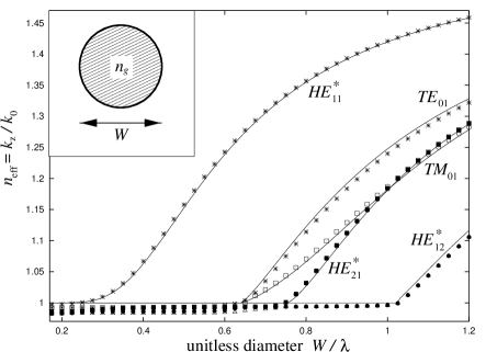
No analytic solution exists for the general rectangular guide, so we used the finite element method discussed in Section III to solve for the bound mode values and fields as a function of guide dimensions. Figure 2 shows the resulting ‘cut-off curves’, that is, contours of constant in the parameter space . In this example we chose a guide index (typical for a polymer dielectric) and, as a preliminary case, a substrate index .
The single-mode region, in which we wish to remain, is bounded below by the and curves and above by the curve. Note that, as in any dielectric guiding structure uniform in the z axis, the lowest two modes ( and in our case) never truly reach cut-off, rather, they approach it exponentially as the guide cross-section is shrunk to zero. For this reason, we chose the practical definition of cut-off for these modes to be , which corresponds to only about 20% of the power being carried inside the guide. In contrast, higher modes do have true cut-offs[31, 30] (this distinction is illustrated by the dispersion curves of Figure 4), and for the mode our (numerically limited) contour choice of falls very close to the true cut-off curve.
Using the numerically calculated electric field strengths of the and modes, we found the red and blue guided laser powers which gave the deepest trap, subject to the constraint of fixed total power (keeping the detuning constant [32]). We also imposed the restriction that the zero of trapping potential come no closer than 100 nm along the vertical line , which kept the trap minimum a reasonable distance from the surface (see Section IV A). Performing this optimization over a region of the parameter space covering the single-mode region gave a contour plot of maximum achievable depth for a given total power, shown within the rectangle overlayed on Figure 2. This depth increases from negligible values in the top left to the largest depths in the lower right, indicating that choosing and to be in this latter corner of the single-mode region is best for depth. The depth shows very little variation with in this corner, rather it is clear that varying to stay within our definition of the single-mode region has become the limiting factor on achievable depth. We indicate a practical choice of and as a small marker on Figure 2. Example trapping potentials shapes possible with these parameters are shown in Figure 3; we discuss their properties in Section II.
In Figure 1a the direct excitation of the optical guide by the two laser beams is shown only schematically. In a realistic experimental setup this coupling into the guide would happen on the order of a centimeter from the atom guiding region, and could involve tapered or Bragg couplers[30] from beams or from other fibers. At this distance we estimate that isotropic stray light due to an insertion loss of 0.5 would have 8 orders of magnitude less intensity than the EW fields in the guiding region. Assuming the light is coherent, this limits the fractional modulation of the guiding potential to . More improvements are possible, including the use of absorbing shields, bending the guide through large angles away from the original coupling direction, and reducing the coherence length.
C Discussion of optical cut-off and substrate choice
We have shown in Figure 2 that parameters optimized for trap depth are near optical cut-off. It is worth gathering together the physical reasons for this. Firstly, on general geometric grounds, the typical available intensities in a guide scale inversely with the effective cross-sectional area of the bound mode, which, far from cut-off (that is, when ) follows very closely the cross-sectional area of the guide. This makes it favorable to shrink guiding structures to areas less than a square wavelength, where they generally become single-mode. Secondly, once we’re in the single-mode regime, as we approach cut-off the mode power is carried increasingly outside the guide, increasing the ratio of surface intensity to guide center intensity. Thirdly, the evanescent decay length in the vacuum is longer as we approach cut-off (recall that in the case of the slab, this is exactly expressed by [30], where the factor of 2 arises because we are considering intensity decay length rather than amplitude). In the special case of , the decay length diverges to infinity as we approach cut-off. Finally, the ratio becomes larger as we approach cut-off, with corresponding beneficial effects on depth and coherence (due to increasing the ‘goodness factor’ we will introduce in Section II A).
Unfortunately, these purely theoretical reasons for approaching cut-off are in opposition to more practical ones. The closer to cut-off a guide is, the more sensitive it is to manufacturing variations in cross-section: in our case this will be predominantly a sensitivity to . The result is that small variations in cause large variations in mode size, or, at worst, complete cut-off. If the mode size change is rapid (nonadiabatic) along the z axis, (for instance if this change is due to surface roughness or refractive index inhomogeneities) the resulting mismatches will be a source of scattering of the guided power. Any coherent scattering back down the guide will set up periodic modulations of the light field over long distances. (One way to reduce the distance over which coherent addition is possible is to use very broad line-width light sources, which would dramatically reduce modulations due to both guided and stray scattered light). The consequence for the atoms would be a z-dependent trap depth and shape, and this could lead to partial reflection or even localization of the matter waves. In general we expect scattering to limit how close to cut-off we can reliably operate.
With regard to the substrate, further practical issues arise. In the above cut-off calculation we chose the simplest case of , corresponding to a guide surrounded by vacuum. A real substrate with has the unfortunate effect of limiting the propagation constant of strictly bound modes to be larger than the freely propagating wavevector in the substrate; in other words, must hold or the light field will rapidly tunnel into the ‘attractive potential’ of the substrate. This in turn limits the decay lengths and that can be achieved. The trap properties quoted in the abstract and in Sections II A and II B paper rely on very low values (1.07 for the mode, 1.18 for ) for the reason that a low is the only way to create long evanescent decay lengths in the vacuum. (This is equivalent to Ovchinnikov et al. choosing reflection angles very close to critical[16].) However, in Section II C we present preliminary results for a substrate of sodium fluoride (the lowest-index common optical mineral, at ), and do not believe the substrate alters the basic feasibility of our waveguide.
For completeness, here we list some other possible approaches to the substrate issue. 1) Use an aerogel substrate, which can have exceptionally low refractive indices and low loss (films of several m thickness with indices of about 1.1 can be produced[35]). 2) Use a dielectric multilayer substrate with an effective index of unity or less (very low loss multilayer mirrors[33] with effective indices less than unity can be created). 3) Investigate if there exist guide shapes which have sufficiently small tunnelling rate into a conventional substrate that the fact that the modes are not strictly bound becomes irrelevant (for instance, a wedge shape with the smallest face in contact with the substrate). 4) Unsupported guiding structures could be produced over short distances[34]. Finally, it is important to note that the idea of replacing the substrate by a metallic reflective layer is not practical because they are too lossy.
Ultimately, the best values of and , the best guide cross-sectional shape, and the substrate choice will depend on many of the above factors and is an area for further research.
II Trap properties
In the bulk of this Section we will examine the atomic waveguide properties for light nearly resonant with the D2 line of cesium, using an optical guide of index 1.56 of the dimensions and from Section I B, and a substrate of unity index. The saturation intensity for cesium is 11.2 W/m2 [10], and its resonant wavelength of 852 nm requires that the physical guide size is 0.83 m by 0.21 m. (At the end of the Section we present preliminary calculations for a substrate and a different guide, and discuss how the atom waveguide properties are changed).
Given the guide, we are free to choose three experimental parameters, namely the optical powers carried in the two modes, and the detuning (assumed to be symmetric, that is, to be of equal magnitude for red and blue beams, because little advantage can be gained with an unsymmetric detuning). The first two of these can usefully be reexpressed as total power , and the power ratio . The trap shape will be affected by alone: we show the trapping potential shapes achievable at the two practical extremes of and in Figure 3, where we have chosen and to give identical trap depths and coherence times. Smaller values cause the trap minimum to move further from the surface (a distinct advantage), to be less “bean” shaped (i.e. to have smaller cubic deviations from a 2D harmonic oscillator), and to cause a slight increase in collection area. It is possible to achieve a trap minimum as distant as from the surface when . The only disadvantage to implementing these smaller values is that a higher is required to achieve the same trap depth and coherence time (for instance a factor of 7.5 increase is required as we take from 0.4 to 0.2). This can be quantified within the exponential approximation, and it can be found that the total power required to maintain a given depth and coherence time with a fixed trap geometry scales as .
If we were purely interested in maximizing trap depth at a given and detuning, it would be best to make as large as possible, however if we take much larger than 0.4 the trap is brought so close that the corners of the “bean” shape touch the dielectric surface (see Figure 3, upper plot) and we will lose effective collection area due to sticking of atoms onto this surface.
A Depth, coherence time, and Q factor
We may ask what trade-offs are necessary between trap depth and coherence time. It turns out that, within the exponential approximation (7), this is elegantly quantifyable. We can define a ‘goodness factor’
| (9) |
where the trap minimum position is at , and the second equality is verified by substitution of (5) and (6), and defining and . We use this latter definition because we are interested in the coherence time of atoms spending time close to the trap minimum (which will certainly be true for the transverse ground state.) Using (7) to solve for and evaluate the ‘goodness factor’, it turns out that the factor is independent of either laser power (i.e. of either or ), giving
| (10) |
| (11) |
fixing the product of achievable depth and coherence time as a constant multiple of the detuning. This is a remarkable result since it shows that increasing is really the only objective in the field design of two-color EW traps. We can write this in units more convenient for cesium trap design, thus,
| (12) | |||||
| (13) |
where the value (taken from best-fit exponentials to the numerically-found squared electric fields for the guide dimensions of Section I B with ) has been substituted to give the the final form. This design expression does not give the required to reach a desired balance between and , however, the total laser power is usually in the mW range, several orders of magnitude less than in most free-space trap designs. For instance, with mW, and nm we could generate a trap of 2 mK depth with the relatively short coherence time of 0.9 ms. The transverse oscillation frequencies in this trap would be kHz and kHz (the field shapes fix this ratio at about 1:4), giving an atomic mode spacing due to the x motion of 5.6 K, roughly twice the cesium MOT temperature, and a characteristic ground-state size of 26 nm by 12 nm.
For coherent guiding, we can define a more physically meaningful figure of merit, , which tells us the typical number of coherent transverse oscillations we can expect multiplied by (i.e. it is the Q-factor of the transverse oscillations). We should choose since this is the smaller of the transverse frequencies in our case. For the transverse atomic modes will be well resolved, and our guide can be a useful interferometric device. Using (11), in conjunction with the fact that when the trapping potential shape is fixed then is proportional to the square root of the depth, tells us that for a given trap and detuning, . For a higher we should choose smaller transverse oscillation frequencies, that is, shallower traps. For example, the 2 mK trap discussed above has , but if we reduce it to a 20 K trap of the same (by changing or the laser powers), the is 10 times larger. Increasing would allow even higher to be realized.
The dependence on detuning in (12) is another way of expressing the advantages already known about using far off-resonant beams[10, 5]. However, our single-resonance approximation will break down if the detuning is too large: we have (somewhat arbitrarily) chosen a detuning limit of 15 nm, as compared to nm for cesium. At this limit, the additional dipole potential created due to the detunings from the D1 line is very significant. However, by removing the detuning symmetry (changing from +15 nm to +12.07 nm and from -15 nm to -17.14 nm), the desired D2 single-resonance approximation potential is recovered in the true physical situation of both resonances present. (These required shifts, which are of order , can easily be found using the expression for the sum of dipole potentials from the two lines.) An additional necessity for our limit is the fact that any larger detunings start to demand separate bound-mode calculations for the two colors, a treatment we reserve for the future. This detuning limit in turn limits the depths, coherence times and Q-factors we quote here, but we anticipate similar future EW atom waveguide designs which explore the region (or even ), and achieve much better coherence.
B Other properties
We estimate the collection area of the trap as the cross-sectional region within which the potential is deeper than the typical cesium MOT energy . For our example 100 K traps of Figure 3 this area is about 1 m2. However, it is not possible to do much better than this with our design: if one tries to increase the area by increasing the overall trap depth, the contour touches the substrate, indicating that atoms at this energy can reach the substrate surface, where they will stick, limiting the effective collection area.
To investigate the lifetime of atoms transported incoherently (the multi-mode regime), we can calculate the heating rate along similar lines as Grimm and Weidemüller[5]. We start with their equation (23) which gives the rate of change of the average of the total energy of atomic motion as
| (14) |
being the recoil temperature, and use the assumption that in an equilibrated 3D trap . Since there is harmonic motion in two directions but free motion in the third, the virial theorem gives us . Combining this with from (9) gives the heating rate
| (15) |
which is of the order of one recoil temperature per coherence time. For our 100 K depth trap at nm the rate is 4.4 K s-1, implying that storage and transport for many seconds is possible. For simplicity, we have ignored the fact that there may be distinct longitudinal and transverse temperatures which do not equilibrate over the trapping timescales.
C Effect of a realistic substrate
In this section we present calculations, performed using the method of Section III, for a practical substrate choice of sodium fluoride (the lowest refractive index common mineral, with at a wavelength of 852 nm), and investigate how this changes the atom waveguide properties from those presented above. We increased to 1.7 (dense flint glass, e.g. BaSF type) in order to provide sufficient index difference from the substrate.
Fixing the width at , we found that a height gave the largest of , and allowed both modes to be sufficiently far from cut-off (greater than half the power being carried inside the guide for both modes). The result is a goodness factor which is approximately half that of the case, with a corresponding halving of the achievable product of depth and coherence time according to (12), and doubling of the heating rate at a given and according to (15). The shorter decay lengths of 56 nm and 68 nm (compared to 93 nm and 137 nm for ) cause the typical trapping distance to be reduced by a factor of roughly 1.8.
We found that in order to reproduce the depth of K and m of the upper trap of Figure 3 (with unchanged) we needed mW, giving ms. The large power increase over the 1ṁW required for is explained by the fact that this is now towards the upper limit practically achievable rather than the lower. (If is instead scaled in proportion to the new decay lengths, the required increase in is only a factor 1.7). In this example, we find the transverse oscillation frequencies have increased to kHz and kHz, compared to the original kHz and kHz. The increase in is explained entirely by the shorter decay lengths, and the increase in (by a factor of over 3) is attributed to tighter optical mode shapes. It is clear that this latter effect outweighs the decrease in , implying that the inclusion of the substrate has actually increased by 50%.
In summary, the effects of including a realistic substrate limit the maximum trapping distance that can be achieved (because of the reduction in decay lengths), lower the goodness factor, increase the heating rate and the required optical power, but also increase the oscillation frequencies. For our substrate choice, each of these changes was approximately a factor of 2, and we believe that they do not alter the basic practicality of implementing our proposed waveguide.
III Numerical solution of the light fields
The detailed electric field distribution is very important in calculating the trapping potential above the waveguide. An approximation to the form of the fields in the y direction is given by the analytically-known solution for the slab waveguide, but to get more accuracy and knowledge of the full potential shape in the x-y plane, we used a full-vector finite element calculation.
The technique represents the electric and magnetic fields as simple piecewise functions over many “elements” (regions) subdividing a slice through the guide and surrounding media in the xy plane, therefore by a finite number of degrees of freedom. Each element has a dielectric constant associated with it, allowing arbitrary stepwise refractive index distributions in the xy plane to be modelled. Maxwell’s equations for propagating solutions of the form are reduced to a generalized sparse eigenvalue equation with as the eigenvalue and the bound mode field distributions as the eigenvectors [38]. Specifically, we used the technique of Fernandez and Lu [36], with and as the field degrees of freedom, for simplicity using first-order (bilinear) functions to represent these fields over a non-uniform but separable rectangular grid of elements. This required a generalization of the Fernandez and Lu implementation, and careful consideration of their line-integral terms (which are non-standard for a finite element formulation) [39]. Of the many available finite element approaches to dielectric waveguide mode solving, this frequency-domain method was chosen for its absence of ‘spurious modes’, its ability to handle index step discontinuities, its small number of required degrees of freedom and its matrix sparsity[37].
Rather than emulating a radiative boundary condition (a notoriously hard task usually requiring an iterative procedure due to the dependence), we enclosed the problem in a large, perfectly-conducting box of sufficient size that the bound mode evanescent fields were negligible on its walls, making the nature of the boundary condition irrelevant. However, the average level spacing of the unbound modes (the ‘continuum’) decreases with increasing box size, and especially near cut-off this increases the number of iterations required to solve the eigenvalue problem to a given accuracy (we used the well-known ARPACK solver to find the 11 lowest eigenmodes of the sparse matrix). We found that a box size of to gave the best compromise between accuracy and speed. Our non-uniform elements allowed us to have a high element density across the waveguide and in the trapping region, but a low density over the much larger box area, keeping the total number of degrees of freedom manageable.
The fractional error in the propagation constant was less than , and the accuracy of the electric field strengths in the trapping region , when we used elements. This was sufficiently accurate for the present work. Finding the bound modes of each waveguide parameter choice typically took between 3 and 20 minutes of computing time on a Silicon Graphics R8000 processor, depending on how close to cut-off the guide was. We tested the accuracy of the method by solving a cylindrical guide in an identical fashion with the same and a very similar non-uniform grid, for which there are known field solutions [31]. Figure 4 shows the propagation constant agrees with the analytics to within 1%, even close to cut-off. The convergence with was measured for the rectangular guide case, and found to be with . This is less than optimal for first-order elements (which have a maximum possible convergence of ), and is believed to be due to an inability of the bilinear functions to represent physical in-plane and components at dielectric steps, or the weak field singularities which can physically occur at any exterior dielectric sharp edges (regardless of whether acute or obtuse)[39].
Future improvements to the method, which would increase the accuracy or the convergence rate , include using higher order elements (if done carefully, this could correctly represent physical and components at dielectric steps), and explicit modelling of the field singularities at guide corners using specialized elements.
IV Further decoherence and loss mechanisms
A Effects of surface interactions
The EW trap has the benefit of creating high field gradients near a surface, but along with this comes the disadvantage that interactions with that surface that can alter the trap potential and even cause heating and loss of trapped atoms.
An atom’s change in potential near a surface is known as the van der Waals interaction () or the Casimir interaction (), depending on the distance from the surface compared to , the dominant wavelength responsible for the polarizability of the atom (in our case of Cs this is the D line resonance, the same as our trapping resonance). There is a smooth cross-over from van der Waals (, which can be viewed as the atom’s electrostatic interaction with the image of its own fluctuating dipole) to Casimir (, which can be viewed as a retarded van der Waals attraction or equally well as an atomic level shift due to a cavity QED effect) at [40]. In the case of a perfect mirror surface, the full form is known for any , but for a dielectric surface, the expression becomes much more complicated to evaluate[41].
Since our trapping distances are larger than this cross-over point, we will use the Casimir form, which is correct for asymptotically large , and is always an overestimate of the true potential[40]. The dependence of the coefficient with dielectric constant is complicated [42, 44], but we will use the simpler approximate form given by Spruch and Tikochinsky[41], to give
| (16) |
(in the MKSA system). This approximate form is known to be within 6% of the exact expression for any dielectric constant [44]. Substituting the recently calculated[43] static polarizability of cesium, a.u., gives a Casimir interaction coefficient of 4.9 nK m4 for .
Figure 1b shows the effect of this potential on a typical trap of depth 150 K and distance nm. It is clear that the change is negligible further than 100 nm from the surface, and a WKB tunneling calculation along this straight-line path (at ) shows that even if all atoms that reach the surface stick, the loss rate from the first few transverse modes is entirely negligible. However, care should be taken with the multi-mode regime, or in the case of high- traps, since the tunneling via the corners of the “bean” shape may dominate for (Figure 3).
The issue of energy transfer to trapped atoms due to a finite (and possibly room) temperature nearby surface is far less well understood, and may be a problem with many surface-based particle traps, as discussed by Henkel and Wilkens [45]. However, since we are trapping neutral particles and the conductivity of our surface is low, we expect a decoherence rate negligible compared to that already present from spontaneous absorption and emission cycles.
B Bending the waveguide
It would be very useful to be able to carry atom beams along curved paths, by bending our atom waveguide in the plane of the substrate, without significant atom loss. Here we briefly estimate three limitations on the waveguide minimum bending radius (in decreasing order of leniency): 1) the limit imposed by optical radiation leakage, 2) the limit needed for incoherent atom transport, and 3) the limit needed for coherent atom transport in the transverse groundstate. This will give us an idea of the practicality of curved atomic guides.
Firstly, whenever a dielectric optical guide has curvature, there is a loss rate (exponentially small in the curvature radius ), which can be viewed as tunneling out of the guide’s ‘potential well’ induced by the addition of an effective centrifugal potential. In the limit , the effective potential is linear with x (the radial coordinate), and the fractional loss per radian of curvature can be estimated[46], for instance using the one-dimensional WKB formula, to be
| (17) |
where is the evanescent decay length in the radial direction, and is a constant of order unity. Therefore for negligible light loss at a bend we need , typically a couple of tens of microns. This is so small chiefly because we are using an optical guide with a large refractive index step[30].
Secondly, we consider atom loss from an incoherent beam with a transverse temperature (assumed small compared to the trap depth magnitude ), and a longitudinal kinetic energy . We call the approximate spatial extent of the trap potential in the x direction , and restrict ourselves to one-dimensional classical motion in this direction. When in a region of radius of curvature , an effective centrifugal term adds to the trapping potential giving . This causes the atoms to ‘slosh’ towards positive x, only ever returning if there exists a point where for . We can estimate that this will happen if , giving our lower limit on as . In our design m, so if we choose mm we can expect loss-free transport of a beam at a longitudinal kinetic energy up to times the trap depth.
Thirdly, to model coherent matter-wave propagation along a curved guide, we consider the amplitude for remaining in the transverse ground-state, having passed into a curved section and back into a straight section. If again we assume one-dimensional x motion, and assume a harmonic potential around the trap minimum, then the effect of curvature is to shift the minimum position from to . If this shift is much less than the characteristic ground-state size then the projection at each transition will be high, resulting in high flux transmission coefficient. This gives as our condition, which for mK (that is, ms-1) and kHz corresponds to mm. This limit is very conservative since we have not yet made use of the adiabatic condition (where is the rate of change of direction of the guided atom), to design a waveguide path without discontinuities in the curvature.
In conclusion, we have shown that it is possible to bend atoms both incoherently and coherently through large angles on a compact substrate structure of a few millimeters in size.
V Conclusion
We have presented a novel substrate-based neutral atom waveguide, based on the optical dipole force, which combines the features of a planar far-detuned two-color evanescent trap[16] with the ability to confine strongly along two axes. We utilized the differing vertical decay lengths of the two bound-mode polarizations of a submicron-sized optical waveguide near cut-off. We have shown that only a few milliwatts of guided laser power can create atomic potential depths K with transverse oscillation frequencies kHz, a coherence time ms and a trap minimum 200-400 nm above the optical guide surface, for Cs atoms in the state. Laser powers greater than ten milliwatts can give a transverse mode spacing greater than the temperature of a Cs MOT, opening up the single-mode waveguide regime. The advantages of guiding optical trapping fields on a substrate include mechanical stability and reliability, mass production and the potential for transport along complicated paths.
We have given some design criteria for guided-lightwave two-color atom waveguides (chiefly the maximization of the evanescent decay lengths, and of their normalized difference ), and shown that a substrate of low refractive index can be very beneficial. We modelled in detail the trapping potentials for a general rectangular guide of index 1.56 above a unity-index substrate, and have shown that a realistic substrate choice of index 1.32 poses few problems to the viability of the device. We predict that the effect of the surface interaction is generally small, and that coherent guiding is possible around corners of radii mm for a longitudinal velocity ms-1. We also believe that the magnetic part of the potential felt by nonzero atoms could be used to increase the depth and oscillation frequencies further.
This preliminary work (specifically equation (11)) indicates that utilizing detunings much larger than the 15 nm we limit ouselves to here will be very advantageous for coherent guiding. We have only scratched the surface of the design variations possible; for instance, equalizing the horizontal and vertical oscillation frequencies is yet to be attempted. The use of two polarizations is our solution to the problem of maximizing when the detuning is very small compared to the wavelength, but we suspect that there will exist other fruitful schemes where these are comparable (, very far-detuning) and where a large is caused simply by the different optical cut-off conditions at the two wavelengths. We have reserved investigation of cooling schemes for future work (although this has already been demonstrated in an EW mirror[47] and proposed in EW traps[48]). We believe that the potential shapes capable of being produced by guided waves on a substrate also include the possibility of funnel-type loading schemes and coherent atom couplers, allowing for a complete “integrated” atom-optical experiment on a substrate.
Acknowledgements.
It our pleasure to thank J. Thywissen, J. Babb, N. Dekker, V. Lorent, and the members of the Heller Group for fruitful discussions. AHB would also like to thank Prof E. J. Heller for computing resources. This work was supported by the National Science Foundation, on grant numbers CHE-9610501 and PHY-9732449.REFERENCES
- [1] electronic mail address: barnett@tornado.harvard.edu
- [2] present address: IGEN International Inc., 16020 Industrial Drive, Gaithersburg, MD 20877.
- [3] present address: Department of Physics, University of California Berkeley, CA 94720.
- [4] S. Chu, Rev. Mod. Phys. 70, 685 (1998); C. Cohen-Tannoudji, ibid. 70, 707 (1998); W. D. Phillips, ibid. 70, 721 (1998).
- [5] For a review of dipole-force atom trapping, see: R. Grimm, M. Weidemüller, and Yu. B. Ovchinnikov, Adv. At. Mol. Opt. Phys. (to be published), [physics/9902072].
- [6] A. Ashkin, Phys. Rev. Lett. 24, 156 (1970); S. Kawata and T. Sugiura, Opt. Lett. 17, 772 (1992); for a review see A. Ashkin, Proc Natl. Acad. Sci. USA 94, 4853 (1997).
- [7] For an introduction, see: T. Bergeman, G. Erez, and H. J. Metcalf, Phys. Rev. A 35, 1535 (1987).
- [8] J. D. Weinstein and K. G. Libbrecht, Phys. Rev. A 52, 4004 (1995); E. A. Hinds, M. G. Boshier, and I. G. Hughes, Phys. Rev. Lett. 80, 645 (1998); J. Fortagh, A. Grossmann, C. Zimmermann, and T. W. Hänsch, ibid. 81, 5310 (1998); J. Denschlag, D. Cassettari, and J. Schmiedmayer, ibid 82, 2014 (1999).
- [9] J. H. Thywissen, M. Olshanii, G. Zabow, M. Drndić, K. S. Johnson, R. M. Westervelt, and M. Prentiss, Euro. Phys. J. D 7 (1999) (to be published).
- [10] C. S. Adams, M. Sigel, and J. Mlynek, Phys. Rep. 240, 143 (1994).
- [11] Our definitions of and correspond to those of C. S. Adams et al. [10].
- [12] M. A. Olshanii, Laser Physics 4, 995 (1994).
- [13] For a review of evanescent-wave atom mirrors, see: J. P. Dowling and J. Gea-Banacloche, Adv. At. Mol. Opt. Phys. 37, 1 (1996).
- [14] R. J. Cook and R. K. Hill, Opt. Comm. 43, 258 (1982); V. I. Balykin, V. S. Letokhov, Yu. B. Ovchinnikov, and A. I. Sidorov, Phys. Rev. Lett. 60, 2137 (1988).
- [15] C. G. Aminoff, A. M. Stearne, P. Bouyer, P. Desbiolles, J. Dalibard, and C. Cohen-Tannoudji, Phys. Rev. Lett. 71, 3083 (1993); Yu. B. Ovchinnikov, I. Manek, and R. Grimm, ibid. 79, 2225 (1997).
- [16] Yu. B. Ovchinnikov, S. V. Shul’ga, and V. I. Balykin, J. Phys. B 24, 3173 (1991).
- [17] T. Esslinger, M. Weidemüller, A. Hemmerich, and T. W. Hänsch, Opt. Lett. 18, 450 (1993).
- [18] R. Kaiser, Y. Levy, N. Vansteenkiste, A. Aspect, W. Seifert, D. Leipold, and J. Mlynek, Opt. Commun. 104, 234 (1994); G. Labeyrie, A. Landgragin, J. Von Zanthiert, R. Kaiser, N. Vansteenkiste, C. Westbrook, and A. Aspect, Quant. Semiclass. Opt. 8, 603 (1996).
- [19] H. Mabuchi and J. H. Kimble, Opt. Lett. 19, 749 (1994).
- [20] J. P. Gordon and A. Ashkin, Phy. Rev. A, 21, 1606 (1980).
- [21] C. Cohen-Tannoudji, in Fundamental Systems in Quantum Optics, Proceedings of the Les Houches Summer School 1990, edited by J. Dalibard, J.-M. Raimond, and J. Zinn-Justin (North-Holland, Amsterdam, 1992).
- [22] M. J. Renn, D. Montgomery, O. Vdovin, D. Z. Anderson, C. E. Wieman, and E. A. Cornell, Phys. Rev. Lett. 75, 3253 (1995).
- [23] H. Ito, K. Sakaki, M. Ohtsu, W. Jhe, App. Phys. Lett. 70, 2496 (1997); H. Ito, T. Nakata, K. Sakaki, and M. Ohtsu, ibid. 76, 4500 (1996).
- [24] S. Kawata and T. Tani, Opt. Lett. 21, 1768 (1996).
- [25] M. Olshanii, Phys. Rev. Lett. 81, 938 (1998).
- [26] T. Cheon and T. Shigehara, Phys. Rev. Lett. 82, 2536 (1999).
- [27] W. Ketterle and N.J. van Druten, Phys. Rev. A 54, 656 (1996).
- [28] Following the notation of Fernandez & Lu[36] for rectangular guides, mode has () antinodes in the () direction, and overall polarization axis . However as the symmetry line is approached (see Figure 2), mixing of polarizations occurs for the case and the notation becomes more arbitrary.
- [29] Even though the frequencies will actually differ by a couple of percent because of their detunings, and cause a difference in decay lengths of the correct sign, this effect alone is not large enough to create large values. Future designs with larger detunings, possibly much larger than the fine splitting, may be able to use this effect alone.
- [30] H. Kogelnik, in Guided-Wave Optoelectronics, Second Edition, edited by T. Tamir (Springer-Verlag, 1990).
- [31] E. Snitzer, J. Opt. Soc. Am. 51, 491 (1961).
- [32] We made the assumption that the positive and negative detunings caused negligible shifts in the wavelength used for the bound mode calculation. For the largest detunings used in this paper the fractional shift is 1.8%.
- [33] G. Rempe, R. J. Thompson, H. J. Kimble, and R. Lalezari, Opt. Lett. 17, 363 (1992).
- [34] T. A. Savas, S. N. Shah, M. L. Schattenburg, J. M. Carter, and H. I. Smith, J. Vac. Sci. Technol. B 13, 2732 (1995).
- [35] P. Mezza, J. Phalippou, and P. Sempere, J. Non-Cryst. Solids 243, 75 (1999); S. V. Nitta, V. Pisupatti, A. Jain, P. C. Wayner, Jr, W. N. Gill, J. L. Plawsky, J. Vac. Sci. Tech. B 17, 205 (1999).
- [36] Y. Lu and F. A. Fernandez, IEEE Trans. Microwave Theory Tech. 41, 1215 (1993).
- [37] For a comparison of methods, see: S. Selleri and M. Zoboli, J. Opt. Soc. Am. A 14, 1460 (1997).
- [38] J. B. Davies, IEEE Trans. Magn. 29, 1578 (1993).
- [39] A. H. Barnett (unpublished).
- [40] E. A. Hinds and V. Sandoghdar, Phys. Rev. A 43, 398 (1991).
- [41] L. Spruch and Y. Tikochinsky, Phys. Rev. A 48, 4213 (1993).
- [42] I. E. Dzyaloshinskii, E. M. Lifshitz, and L. P. Pitaevskii, Adv. Phys. 10, 165 (1961).
- [43] A. Derevianko, W. R. Johnson, M. S. Safronova, and J. F. Babb, Phys. Rev. Lett. 82, 3589 (1999).
- [44] Z-C. Yan, A. Dalgarno, and J. F. Babb, Phys. Rev. A 55, 2882 (1997).
- [45] C. Henkel and M. Wilkens, Europhys. Lett. (to be published), [quant-ph/9902009].
- [46] For some of the earliest bending loss estimation in a rectangular fiber see: E. A. J. Marcatili, Bell Syst. Tech. J. 48, 2103 (1969); and for the case of a cylindrical fiber, D. Marcuse, J. Opt. Soc. Am. 66, 216 (1976). Most of the work done since then has been on the more complicated situation of fibers with cladding.
- [47] P. Desbiolles, M. Arndt, P. Szriftgiser, and J. Dalibard, Phys. Rev. A 54, 4292 (1996).
- [48] Yu. B. Ovchinnikov, J. Söding, and R. Grimm, JETP Lett. 61, 21(1995); P. Desbiolles and J. Dalibard, Opt. Comm. 132, 540 (1996).