[
DNA - Nanoelectronics: Realization of a Single Electron Tunneling Transistor and a Quantum Bit Element
Abstract
Based on the understanding that chemical bonds can act as tunnel junctions in the Coulomb blockade regime, and on the technical ability to coat a DNA strand with metal, we suggest that DNA can be used to built logical devices. We discuss two explicit examples: a Single Electron Tunneling Transistor (SET) and a Quantum Bit Element. These devices would be literally in the nano-meter scale and would be able to operate at room temperature. In addition they would be identical to each other, highly stable and would have a self assembly property.
pacs:
85.65.+h, 85.30.Wx, 72.80.Le]
The quest for smaller and faster logical devices has persisted since the invention of the classical transistor. A novel idea of using single organic molecules as electronic circuit components has been proposed back in 1974 [1]. However, the difficulty to connect a single molecule to external leads prevented experimental verification of this idea until recently, when molecular junctions (acting as quantum dots) [2]-[4], and a carbon nanotube field-effect transistor [5] have been fabricated.
Here we propose a new approach to make logical devices from molecules, which is based on our understanding [6] that the phosphate bridges in DNA can act as tunnel junctions in the Coulomb blockade regime, and on the technical ability to coat a DNA strand (and other molecules) with metal, thus forming a conductive wire with self assembly property [7]. Our understanding is supported by the observations of Reed et al. [4], who demonstrated experimentally that chemical bonds act as tunnel elements. Combining the above conceptual and technical developments, we suggest to utilize the chemical bonds in DNA (or other molecules) to build logical devices. These would be literally in the nano-meter scale and would be able to operate at room temperature. The operation principle of the proposed devices is the single electron effect, which makes them extremely fast. Since they are made from specific molecules, the devices would be completely identical to each other. They would also be highly stable due to the stability of the chemical bonds. The devices would inherit the self assembly property, which can be used to create complicated networks consisting of many elements.
A DNA strand is made of units (or grains), composed of a sugar and a base. The grains are connected by phosphorus bridges (P-bonds), while complementary bases in different strands are connected by hydrogen bonds (H-bonds). We propose that a P-bond forms a tunnel junction for a net charge [6]. (By ’net’ charge we mean the deviation from the charge distribution of the unperturbed DNA.) The tunneling is either stochastic (like a normal tunnel junction) or coherent (like a mesoscopic Josephson junction), according to the coupling to the environmental degrees of freedom. The origin of this tunnel junction are the two oxygen atoms transversely connected to the phosphorus atom (see Fig. 1). These oxygens share three electrons with the phosphorus, giving rise to two bonds and one bond. As the electron can be shared with both oxygens, it resembles an electron in a double well potential and occupies the lowest level. When an additional electron approaches the well, it encounters a barrier due to the energy gap to the next level of the well. However, since this barrier is narrow and not very high, the approaching electron can tunnel through it.
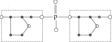
The H-bonds have a capacitive property. The proton in the H-bond can effectively screen a net charge density on either side of the bond by shifting its position towards this side. As a result, the net charge accumulates on the sides of the H-bond, and the bond can be viewed as a capacitor. The grains themselves have inductive properties, stemming from the hopping of additional electrons. The notations are shown in Fig. 2.
According to the picture presented above, the DNA molecule inherently possesses all the properties needed for logical devices. The fabrication of these devices can be done using available DNA manipulation techniques. As an example we show how to build a classical SET transistor (see Fig. 2). One should start with two strands (a main strand and a gate strand), and connect the end base of the gate strand to a complementary base in the middle of the main strand. Both strands should be metal-coated, except the grain in the main strand which is connected to the gate strand, and its two adjacent P-bonds. The connective H-bond should be uncoated as well. To do this, the method presented in Ref. [7] has to be generalized to enable selective coating. We expect it to be feasible if artificially made strands are used, so that the coated and uncoated parts are composed of specific, yet different sequences of bases. Before the coating the DNA molecule should be in solution containing an enzyme which can bound only to the parts which should not be coated. After the coating the enzyme is released, and one obtains the desired result. The metallic coated ends of the main strand can be now connected to a voltage source ,, and the end of the gate strand to another voltage source, , which acts as a gate voltage.


This DNA-made device has the structure of a SET transistor [8], i. e., a grain connected by two tunnel junctions to a voltage source, and biased by a capacitive coupling to a gate voltage. Usually, when discussing the SET transistor, one neglects the inductive properties of the grain. This neglect is equivalent to the claim that the relaxation time in the grain is much shorter than the tunneling time. The values of and in the DNA molecule are not known, but should be very small, probably in the pico Henry range. Thus the relaxation time is very short, and we can neglect the inductances here as well. We also assume that the coupling to the environment is strong such that the tunneling is incoherent. In this case the voltages across the two junctions are
| (1) | |||||
| (2) |
where is the number of surplus electrons in the grain, and is the electron charge. We added suffixes to distinguish between the two tunnel junctions. The instantaneous rate of tunneling from the right across the first junction, say is calculated from the single electron energy levels [9]:
| (4) | |||||
where is the tunneling matrix element for an electron in a state of energy , is the Fermi distribution function, and are the density of states for the grain and the right electrodes, respectively, and similarly and are their highest occupied energies. Their difference gives rise to a Coulomb blockade of tunneling into the grain. The system obeys the Fermi distribution due to the large coupling to the environment. The other tunneling rates: , , and have similar expressions. The probability that there are electrons in the grain at time is governed by the master equation:
| (7) | |||||
where the transition rates (4) are expressed as functions of using (1). The I-V characteristics of the SET are obtained by solving Eq. (7) numerically using the appropriate initial and boundary conditions [8]-[10]. A typical I-V characteristic for constant density of energy states and identical junctions in the low temperature limit has a voltage threshold. In order to operate as an transistor, is varied around the threshold voltage. For well functioning transistor characteristics, the current raise above the threshold value should be as steep as possible. This situation can be achieved if the tunneling rates (or times) of the two junctions are different, or if there is a gap in the density of energy states of the grain. As the DNA molecule is not conductive it possesses a natural energy gap. The gap can be enhanced by using a larger section of DNA containing several grains instead of a single one. This happens since long DNA chains have non-linear effects, resulting in the tendency of charges to form solitons [6]. This method has also the advantage that it is technically easier to leave a larger section of DNA uncoated than a single grain. The tunneling rates in the DNA SET are the same, as the two P-bonds are identical. This situation can be amended by attaching a chemical group to one of the P-bonds, thus altering its properties.
As a second example for DNA-made logical device, we discuss a possible realization of a quantum bit (qubit), which is the fundamental element needed for quantum computation [11]. Several systems which can act as qubits have been recently proposed, included trapped ions [12] and Josephson junctions [13]. The tunneling property of the P-bond enables to use DNA to form a qubit realization similar to the one of Shnirman et al. [13]. Since the main concern in the operation of qubits is maintaining quantum coherence over long periods of time, DNA-made devices can be used for quantum computation when the interaction with the environment is weak. In Fig. 3 we suggest how to build a qubit using three DNA strands: one short strand, containing two sugars and a P-bond in between, and two long metal-coated strands connected to the two sugars by H-bonds. This device has the same structure of a Josephson junction qubit [13], and should operate in the same manner. A detailed study of a DNA-made qubit will be presented elsewhere.
To conclude, we have shown that the DNA molecule has the needed properties to make logical devices. We have discussed specifically how to build a single electron tunneling transistor and a quantum bit element. Due to their nano-scale dimensions, conformity and availability, DNA-made logical devices would have the advantage over the current solid state ones. In addition, the DNA-made devices would operate at room temperature and would have a self assembly property.

This research is supported in part by a GIF grant G-0464-247.07/95.
REFERENCES
- [1] A. Aviram and M. A. Radner, Chem. Phys. Lett. 29, 277 (1974).
- [2] C. Joachim, J. K. Gimzewski, R. R. Schittler and C. Chavy, Phys. Rev. Lett. 74, 2102 (1995).
- [3] D. Porath and O. Millo, J. Appl. Phys. 81, 2241 (1997).
- [4] M. A. Reed, C. Zhou, C. J. Muller, T. P. Burgin and J. M. Tour, Science 278, 252 (1997).
- [5] S. J. Tans, R. M. Verschueren and C. Dekker, Nature 393, 49 (1998).
- [6] E. Ben-Jacob, Z. Hermon and S. Caspi, Europhys. Lett., in press.
- [7] E. Braun, Y. Eichen, U. Sivan and G. Ben-Yoseph, Nature 391, 775 (1998).
- [8] M. Amman, K. Mullen and E. Ben-Jacob, J. Appl. Phys. 65, 339 (1989).
- [9] Tunneling Phenomena in Solids, edited by E. Burnstein and S. Lundqvist, (Plenum Press, New York, 1969).
- [10] M. Amman, R. Wilkins, E. Ben-Jacob, P. D. Marker and R. C. Jaklevic, Phys. Rev. B 43, 1146 (1991).
- [11] A. Barenco, Contemp. Phys. 37, 357 (1996).
- [12] J. I. Cirac and P. Zoller, Phys. Rev. Lett. 74, 4091 (1995).
- [13] A. Shnirman, G. Schön and Z. Hermon, Phys. Rev. Lett. 79, 2371 (1997).