Properties of CsI(Tl) Crystals and their Optimization for Calorimetry of High Energy Photons ††thanks: Work supported by BMBF under contract No. 06 DD 558 I
TUD-IKTP/98-01
A photomultiplier setup for precise relative CsI(Tl) crystal light yield and uniformity measurements is described. It is used for wrapping material studies to optimize the uniformity and the yield of the light output of long crystals. The uniformity is an important property in high energy photon calorimetry. Results of an optimization of photodiode coupling to crystals, the influence of temperature and radiation damage to light and photoelectron yield are also presented.
1 Introduction
Although Thallium doped CsI crystals are widely used in high energy physics
detectors [1, 2], new precision experiments at the
B-meson factories presently under construction [3, 4]
rely on CsI(Tl) calorimeters with improved energy resolution, electronic noise,
and crystal radiation hardness. The energy resolution at low energies is
influenced by the (temperature dependent) crystal light yield, which should be
stable over long time periods and maximized to achieve low electronic
noise [3].
Because of fluctuations of electromagnetic showers in the crystals it is
necessary to know and to optimize the uniformity of light output. Related
studies can be found in the literature
[5, 6, 7], but there are often
descrepancies between laboratory studies performed with photomultipliers
and the actual photodiode readout used in calorimeters. One reason is the
very different sensitivity of both readout devices at the wavelength of the
CsI(Tl) scintillation light.
We will limit ourselves to investigations which are relevant for large high energy physics calorimeters. After introducing setups, which allow comparable and precise crystal measurements with photomultipliers and photodiodes, we describe a method to improve the crystal light yield and response uniformity. Using light yield optimized crystals we studied several ways to couple photodiodes to crystals and to enhance the photoelectron yield thereby minimizing the equivalent electronic noise energy. Since temperature and radiation can alter the crystal light yield, their influence was investigated with both readout setups. These investigations were performed as part of early studies for the electromagnetic calorimeter of the BABAR detector.
2 Experimental Setup
The CsI(Tl) crystals used in this study were supplied by Monokristal/Kharkov (Ukraine). Their Thallium content amounts to . The crystals were slightly tapered with a front face of , rear face dimensions of , and a length of , which corresponds to 19.4 radiation lengths.
2.1 Photomultiplier Readout
The scintillation light of CsI(Tl) with a peak emission wavelength at
was read out using a Hamamatsu R669 photomultiplier tube with a
multialkali photocathode ( diameter), which has an enhanced sensitivity
in this wavelength range [8, 9].
The photomultiplier, which was coupled to the crystals via a minimal airgap, was operated at (anode grounded), and read out by AC coupling to an Ortec preamplifier model 113 with an input capacity of . A spectroscopic amplifier, Ortec model 672, provided a Gaussian shaping with time constant and an additional amplification. A peak sensitive ADC, Ortec 800, was DC coupled to the amplifier in order to avoid an additional differentiation of the pulse at the ADC input. For pile-up rejection the corresponding signal from the shaping amplifier was fed into the ADC. A PC based multichannel analyzer from Target with the corresponding TMCA software was used for data acquisition.
For position dependent measurements of the light output, a radioactive source with a lead collimator was moved along the length of the crystal. The energy of the source, the collimator outer dimensions, and the pin-hole diameter of the collimator were optimized in order to get a focused illumination at the crystal surface and a sufficient penetration depth. Finally the collimator was laid out as an almost half-sphere with radius and a pin-hole diameter of . It was located above the crystal surface and contained
a 137Cs source with and energy. These parameters resulted in a mean spot diameter at the crystal surface of as shown in Fig. 1.
A step-width of was chosen for the motorized translation stage moving the collimator because of the spot size. At each collimator position a dead-time corrected spectrum was taken for 100 seconds, resulting in a total measurement time of about half an hour for 18 positions along the crystal. The region of the photopeak was fit to the sum of a Gaussian distribution and an exponential background.
In order to quote a crystal light yield, the 18 peak positions were averaged and related to the position of the corresponding peak for a small cubic CsI(Tl) crystal ( on an edge). This standard crystal was remeasured regularly. Thus, total light yield LY values given in this article are relative to this standard crystal.

For precise measurements of different crystals, independent of photomultiplier drift, gain variations, and environmental influences, two different monitoring systems were developed. One consisted of an 241Am source placed on a small hole in the crystal wrapping material at the front end of the crystal. This source emits -particles with an energy of about , which generate a constant amount of scintillation light in the crystal. Fig. 2 shows a pulse height spectrum of a 137Cs -source with a 241Am -source as reference attached to a large crystal. When the crystal is scanned with the 137Cs -source, the variations of the position of the -peak indicate drift of the electronics during the uniformity measurement, which is corrected during the analysis [10].
For this monitoring method, the error of the peak position was for spectra taken along one crystal, mainly due to the description of the background. However, the error for the total light yield of a particular crystal is much larger, since the -line position may vary from crystal to crystal owing to variations in light generation and transmission. Therefore, an external reference system was developed and operated under stable and controlled conditions.
This system used a “light normal” consisting of an encapsulated combination of a NaI(Tl) crystal and a 241Am source. Since the light output of this crystal is low, its light cannot directly be coupled to the R669 photomultiplier. Instead, it is detected by another photomultiplier (Philips RCA 8575), which is in addition illuminated by a green LED. The LED is pulsed by an adjustable voltage and frequency. This setup is located in a light tight, temperature stabilized box. A fixed fraction of the LED light is fed, via a long glass fiber with negligible temperature dependence, into the entrance window of the R669 photomultiplier which measures the CsI(Tl) crystals. A sketch of the setup is shown in Fig. 3.
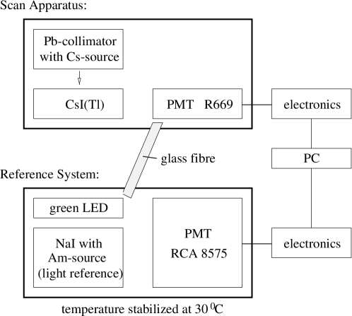
Variations in the LED light and in the gain of the photomultiplier of the reference system are corrected by the output of the light normal. In this way an error of better than for the total crystal light yield was achieved and verified by long-term comparisons of a few crystals.
At this level of accuracy, the temperature dependence of the crystal light yield becomes important. Therefore the crystals were located in a styrofoam box and temperature sensors were attached on the wrapping material. The light yield for each crystal was corrected by the measured temperature dependence of the light output (see section 4).
2.2 Photodiode Readout
For the light readout by photodiodes, radioactive sources of higher photon energy are required. We have chosen 88Y with and . The scintillation light is read out by two PIN silicon photodiodes coupled to the crystal rear. Two different types of photodiodes from Hamamatsu were used, S 2744-08 with an active window size of for direct readout and S 3588-03 (mod 5400) with an active area of for wavelength shifter readout. These types have an active layer of thickness and are SiN passivated. The diodes are operated with a reverse bias voltage of with the cathode grounded. Typical values for the dark current of and for the capacity of () are reported by the manufacturer for the types S 2744-08 and S 3588-03 (mod 5400), respectively. We measured the dark current of an initial sample of 110 diodes of type S 2744-08 in a temperature controlled environment using a Keithley pA-meter to be . The same device was used for a measurement of the diode capacity. Thereto a rectangular generator was set up using the diode as a capacitor determining the frequency of the generator. This frequency was converted into a voltage which was measured as a current over a resistor. The result was for 110 diodes.
The quantum efficiency of both types are 85% (90%) at () [11].
The optical coupling of the diodes to the crystal was varied and will be described in section 3.3. The photoelectron yields of both photodiodes were measured individually by independent electronic readout chains [12, 13]. In order to amplify the small pulses typically between 5000 and 8000 photoelectrons for a source energy of , charge sensitive preamplifiers, Canberra 2003T, were coupled via short co-axial cables to the diodes. Crystal, photodiodes, and preamplifiers were located in a light tight box which also provided an electromagnetic shield. From the preamp output each signal was fed into a spectroscopic shaping amplifier, Canberra AFT 2025, with (Gaussian) shaping time and finally DC coupled into a peak sensitive ADC, Montedel Laben model 8215. The pile-up output of the amplifiers was connected to the corresponding ADC input. The ADC are read out with the same TMCA based DAQ system as used for the photomultiplier setup. The photopeak regions in both pulse-height spectra were fit with a combination of a Gaussian and an exponential in order to determine the peak position.
The ADC channel scale was calibrated in absolute electric charge by using the photodiodes as solid state detectors. The peak position for photons from a 241Am source, directly located at the photodiode, was measured. Those photons, when absorbed in the silicon layer, create one electron-hole pair per deposited photon energy. Therefore, the mean peak position of the photon line, which was determined by a fit of a Gaussian and a linear background in the peak region, corresponds to 16480 created photoelectrons. Thus the photoelectron yield PY of a crystal - photodiode combination, with dimensions , can be determined by the ratio of peak positions of scintillation light and photon conversion in the diode according to
| (1) |
 |
 |
Typical spectra are shown in Fig. 4.
The photoelectron yields of both diodes mounted to one crystal were measured individually and added later in order to quote the photoelectron yield of the crystal - diodes setup. This method allowed the measurement of photoelectron yields in a wide range with an accuracy of . The crystals used for this study had photoelectron yields between
and .
The ratio of the Gaussian peak width and peak position of the 241Am line was used to determine the equivalent noise charge ENC:
| (2) |
Typical RMS values for photodiode types S 2744-08 and S 3588-03 (mod 5400) and the amplification / digitization chain as described above are and , respectively. The equivalent noise energy ENE follows from Eqs. 1 and 2,
| (3) |
Typical RMS values are 120 to depending on crystal light yield.
2.3 Comparison of Photomultiplier and Photodiode Readout
 |
 |
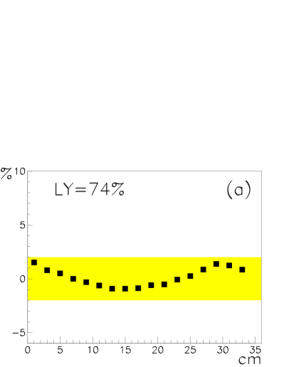
In order to compare the uniformity of a crystal determined with different readout devices as well as to relate the light yield measured with the photomultiplier setup and the photoelectron yield measured with photodiode readout, a uniformity scan with both setups was performed. Since the photon energy of 137Cs is too low to determine the photopeak position with photodiodes, the line of 22Na was used with a modified collimator consisting of two lead blocks with a wide gap. The source was placed in this gap above the crystal surface. The crystal, wrapped in two layers of Tyvek 1056D and aluminized mylar foil (see section 3.1), was first scanned with the setup described in section 2.1 and then with the modified collimator and the 22Na source, which gave identical results within the measurement errors for light yield and uniformity. Finally, two photodiodes S 2744-08 were glued to a 1mm thick lucite plate, which in turn was glued to the center of the crystal rear face. The remaining rear area of the crystal was covered with a reflector, also consisting of Tyvek 1056D. The scan was repeated with the same stepwidth, but using the photodiode readout electronics. Fig. 5 shows a very similar uniformity behaviour and allows the determination of the corresponding photoelectron yield for a given light yield. Here corresponds to . This relation was verified later with a larger number of crystals.
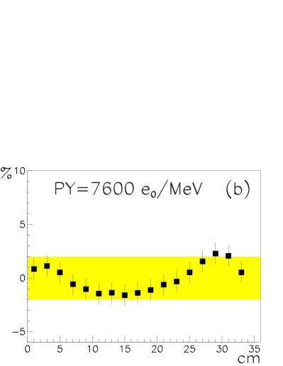
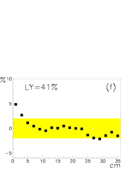
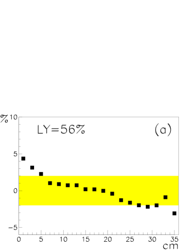
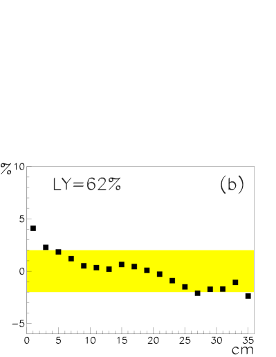
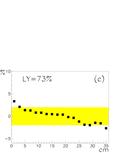
The uniformity of the crystal light output does not depend on the area covered by the readout device, as shown in Fig. 6.
 |
 |
All other photodiode measurements described in the remainder of this article were performed following the prescription of section 2.2 without uniformity scan, whereas all photomultiplier uniformity scans were measured with the monitoring setups as described in section 2.1. The uniformity plots will always have the photomultiplier located at position (the larger crystal area). The plotted values are the relative variation of light yield at a given position from the average yield in percent.
3 Optimization of Crystal Light Yield and Uniformity
In this section the influence of type, quality, and thickness of wrapping material on crystal light yield and uniformity is described. A method to improve the uniformity of the light output is presented. These studies were performed with the photomultiplier setup which gives more precise results. The influence of optical properties of different coupling materials between crystal and photodiodes is described in section 3.3.
3.1 Crystal Wrapping
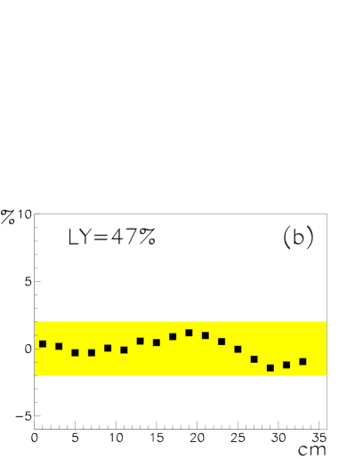
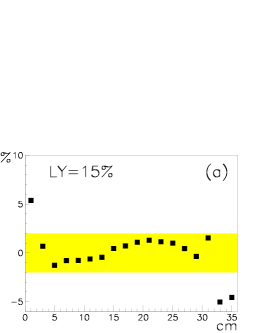
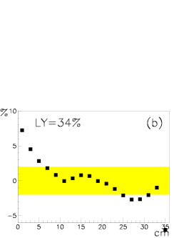
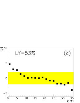
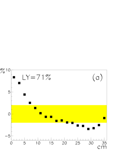
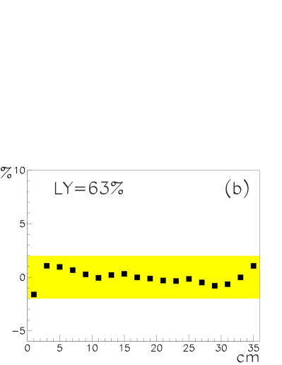
After measuring the light output achieved by only internal reflection of scintillation light in a crystal with surfaces polished by the manufacturer, see Fig. 7(a), consecutive layers of thick Teflon PTFE are added. With more material wrapped around the crystal, the light yield increases and uniformity improves. Using an ideal reflecting thick aluminum foil after three layers of Teflon results in the same total light yield as use of an additional layer of Teflon (Fig. 7(d) and (e)) . The comparison of four layers Teflon ( in total) with one layer of thick Teflon shows that the multilayer configuration gives a higher light yield, Fig. 7(d) and (f).
The gain in light yield and uniformity by adding additional layers of material
is compromised by the increasing amount of dead material between crystals.
 |
 |
 |
 |
 |
 |
Since Teflon PTFE shows an unfavourable longtime behaviour (multilayers tend to be pressed together, thus forming a monolayer with reduced reflecting properties) and is difficult to handle because of its adhesive properties, DuPont Tyvek was investigated as an alternative [9, 14]. This material is a porous, chalk-loaded polyethylene fleece, which is supplied in different qualities and thicknesses. For the Tyvek types 1025D, 1056D, and 1059D total light yield values were measured, which are comparable to the results for multilayers of Teflon of similar total thickness. Fig. 8 shows uniformity plots for one and two layers of Tyvek 1056 D, per layer, with and without an additional aluminum foil layer.
 |
 |
 |
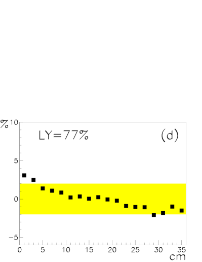 |
With increasing material thickness, the uniformity again improves. The aluminum foil not only gives higher light yield values, but also provides electromagnetic shielding of the crystal.
3.2 Uniformity Tuning
A uniform crystal response is important for the linearity of a detector and the energy resolution, since the position of the shower maximum varies with the incident energy and fluctuates for fixed energies. An additional advantage of Tyvek is the possibility to improve the uniformity of the light output of crystals by changing local absorption properties at the crystal surface without machining the crystal itself. This is done by blackening the Tyvek at appropriate positions. An example is shown in Fig. 9.
 |
 |
3.3 Optical Coupling
Two general types of coupling of the photodiodes to the crystal rear surface were investigated: wavelength shifter and direct readout [12, 13].
3.3.1 Wavelength Shifter Readout
The wavelength shifters consisted of fluorescent dyes, dissolved in thick lucite (PMMA) carrier plates covering the whole crystal rear face. Both investigated types (BASF Lumogen F red 300 and Roehm 2466 P) show similar optical properties (several absorption maxima at about , , and
; fluorescence emission at ), thus effectively collecting the crystal scintillation light and transforming it into a wavelength range where the quantum efficiency of the photodiode is higher (see section 2.2). They had the full size of the crystal rear surface and were coupled via a small () airgap to the crystal. The diodes were glued onto two adjacent narrow sides of the wavelength shifter. The rear area was covered by a diffuse reflecting material (Tyvek), whereas all the lateral faces not equipped with photodiodes were painted with polyurethane based reflective paint NE 561.
The adhesive used to glue the photodiodes S 3588-03 (mod 5400) to the wavelength shifter was Cargille Meltmount with an index of refraction of 1.53, well matched to the corresponding values for PMMA and the entrance window of the photodiodes (both ).
Using two photodiodes on adjacent edges of the wavelength shifter did not double the photoelectron yield compared to the readout with one photodiode, but increased it by a factor of 1.5 only. The second photodiode does not transfer all absorbed light into measureable charge, whereas a reflecting material at position of the second photodiode redirects a part of the light to the first photodiode. This is compared in Table 1 with an absorber ( black Scotch tape) placed at the position of the second photodiode. In this case, the light yield is only two thirds of the value achieved with one photodiode and a reflector.
| 2 photodiodes | 1 photodiode | 1 photodiode | |
|---|---|---|---|
| + reflector | + absorber | ||
| PY | 5900 | 3900 | 2600 |
| ENE | 110 | 115 | 175 |
The maximum photoelectron yield of for two photodiodes was achieved with an octagonal wavelenght shifter with on an edge (= length of photodiode window) and a diameter of between parallel sides. This corresponds to an equivalent noise energy of for the crystal.
3.3.2 Direct Readout
In case of the direct readout the main focus was the search for the best coupling medium between the crystal and the photodiode entrance medium with respect to photoelectron yield and reliability. In order to diminish long-time effects such as migration of ions from the crystal to the diodes active material, which could result in a decrease of the photoelectron yield, additional transparent coupling plates were investigated [13, 15]. Their optical properties are given in Table 2.
| Coupling | Index of |
| Plate | Refraction |
| Bor-Silicate Glass | 1.50 |
| Lucite (PMMA) | 1.50 |
| Lexan (PC) | 1.59 |
| Polystyrene | 1.60 |
Because of the difference in the indices of refraction of the crystal
() and the entrance window of the photodiode ()
materials with higher refractive index are favoured [16]. This is
also the reason for typically lower photoelectron yield in the case of a small
airgap between crystal and photodiodes.
Table 3 shows the various optical adhesives which have been
investigated, and typical ranges of photoelectron yields for a class of adhesives.
Comparing the results in Table 3, optical grease and epoxies give
the highest photoelectron yields. Because of its poor longterm behaviour (it tends to flow and
to change color), optical grease cannot be considered for CsI(Tl) crystal based calorimeters.
The highest photoelectron yields were achieved with the last three epoxies of Table 3. They all have a refractive index of 1.56. Using BC 600 for both glue joints (coupling plate to crystal and photodiodes to coupling plate) the three coupling plate types Lucite, B-Si-Glass, and Polystyrene give very similar photoelectron yields (), whereas Lexan is worse (). Bor-Silicate Glass is very fragile and hard to machine and handle. EPOTEK 301-2 tended towards disconnecting from the crystal over longer time periods ( months). Using the combination photodiodes - BC 600 - lucite plate and testing the three epoxies for the coupling plate - crystal joint, EPILOX A17-01 is slightly favoured ( vs. ). The best result was achieved when using a polystyrene coupling plate and EPILOX for both glue joints (). This corresponds to a equivalent noise energy of , in the same range as in the case of the wavelength shifter readout. The lower photoelectron yield of the latter is compensated by the lower intrinsic noise of the smaller diodes, see Eq. 3. For all measurements the rear area of the crystal surrounding the photodiodes was covered by a diffuse reflecting plate (either Tyvek or reflective paint NE 561). Without these rear reflectors the measured photoelectron yields were about lower.
| optical adhesive | PY |
| Grease | 7000 to 8000 |
| BICRON BC 630 | |
| Rhodosil Silicones Pate B 431 | |
| Silicone Pads | 5000 to 6000 |
| General Electrics GE RTV 615 | |
| BICRON BC 634 | |
| Silicone Glues | 6000 to 6800 |
| General Electrics RTV 108 | |
| General Electrics RTV 118 | |
| Nünchritzer RTV Cenusil | |
| Acrylic Glues | 6500 to 7000 |
| Powa Bond 102 | |
| DELO Photobond 4455 | |
| Loctite 349 | |
| Degussa Agovit 1900 | |
| Roehm Acryfix 200/117 | |
| Forbo Helmitin 21003 | |
| Vitralit 5638 | |
| Epoxies | 7000 to 8500 |
| Ciba Geigy XW 396/397 | |
| Ciba Geigy AY 951/103 | |
| Kodak HE 80 | |
| Lens Bond F65 | |
| Structalit 701 | |
| EPOTEK 301-2 | |
| BICRON BC 600 | |
| EPILOX A17-01 |
4 Temperature Dependence of Crystal Light Yield and Uniformity
Different values for the temperature dependence of the CsI(Tl) light yield are
reported in the literature. In most studies
[7, 17] the light yield dependence was
measured for small crystals in a wide temperature range
( to ) in coarse steps.
These authors report an almost constant crystal light yield between
and .
Here, we concentrate on a comparison of the crystal light yield for photodiode and photomultiplier readout near room temperature, where
large calorimeters are operated [18].
Photomultipliers have their own own temperature dependence, the used type Hamamatsu R669 shows a temperature coefficient of at [8]. However, its influence is corrected by the reference system described in section 2.1. The crystal temperature was varied between and . For these measurements, an airgap of between photocathode and crystal was chosen in order to allow for thermal expansion of the crystal. The photomultiplier was operated at constant temperature, in this way further reducing the measurement errors. The procedure was repeated three times; after the last measurement crystal and photomultiplier were slowly heated to .
In order to get a stabilized coupling of the photodiodes to the crystal, they were glued to the crystal using BICRON BC 600 epoxy and a thick lucite plate and cooled down together with the crystal. Since the temperature dependence of the photosensitivity of the diodes is only at [11], this will not distort the measured crystal properties. Fig. 10 shows the dependence of crystal light yield, normalized to . The crystal temperature coefficients were determined by a straight line fit to the data. The results are for photomultiplier and for photodiode readout, respectively. A reason for the difference between photomultiplier and photodiode readout could be the different spectral sensitivity of both systems, which indicates a decreasing temperature dependence of the scintillation light with longer wavelengths. This would also explain the higher value of found in [5], where a blue-sensitive photomultiplier was used. For photodiode readout these authors find at and report a flat maximum at to . A hint of the latter can be seen in Fig. 10(b).
 |
 |
The uniformity of crystal response did not change in the investigated temperature range.
5 Influence of Radiation Damage on Crystal Light Yield and Uniformity
The influence of radiation damage on the crystal light yield varies strongly
with intrinsic crystal properties (e.g. Thallium concentration, impurities,
absorption length). Therefore, the measured
crystal described below does not represent general CsI(Tl) properties; it merely
shows what kind of measurements and precision can be achieved with the
setups described in section 2 [18].
The front face of a long CsI(Tl) crystal was irradiated several times with increasing dose, using a point like 60Co source, mounted at a fixed distance of . The time between individual irradiations was chosen to be one week, in order to allow for studies of relaxation processes.
The deposited energy dose in the crystal was determined by two independent
dose measurements. At a low dose of about , four LiF
dosimeters with a thickness of were put on the corners of the
crystal front face. The measured dose rate for LiF was
. All following measurements were scaled by the
irradiation time according to this measurement.
In order to check the dose extrapolation at the highest individual dose of
about , four Alanine dosimeters with a thickness of
were put at the same position and a dose rate of
was measured. Owing to the smaller error of the last measurement all other
were scaled by the irradiation time according to this measurement.
In order to get the energy dose deposited at the crystal front face by
photons of and , the
energy doses quoted in this section were evaluated for CsI using
the ratio of the mass energy absorption coefficients for photons of
for CsI ( cm2/g)
and for Alanine ( cm2/g) [19].
During the measurements, radiation doses from about up to in
steps of about a factor of two were deposited at the front face of the crystal.
After each irradiation step, the intensity of phosphorescence light (afterglow) was measured as the anode current of the photomultiplier which was DC-coupled to a voltage/current device. To protect the photocathode, these measurements were started after the phosphorescence light level corresponded to less than anode current at a voltage of . Fig. 11a shows the current measurements after an irradiation of . Fig. 11b shows the dependence of the phoshorescence time constant on the deposited energy dose, defined by . The relaxation times rise from to for doses increasing from to .
 |
 |
The constant currents in the fit of the time dependence increase from
to over this dose range. Repeated measurements
six days after each individual irradiation show values between and
, whereas the value before any irradiation was about .
These measurements indicate additional relaxation time constants for radiation
induced phosphorescence on the order of days.
The influence of the accumulated energy dose on the crystal light yield was investigated with photomultiplier (137Cs source) and photodiode (88Y source) readout. Directly after irradiation, a decrease of the crystal light yield is observed which reaches a constant level a few hours (days) after irradiation with low (higher) doses. Therefore, the light output on the fourth day after irradiation was chosen as a measure for the reduction of light yield after successive irradiations and plotted versus the accumulated energy dose in CsI in Fig. 12. In the case of photodiode readout, the diodes were fixed with a minimal airgap at the crystal rear, in order to prevent radiation damage to the diodes and to allow for alternating photomultiplier and photodiode measurements of the same crystal. Therefore, the measured photoelectron yield is smaller than with glued diodes. The errors are larger because of the reproducibility of the optical coupling.
 |
 |
At an accumulated energy dose of , light reductions of
and are measured with the photomultiplier
and photodiode readout setup, respectively. In repeated measurements during
the week between two irradiations and months after the last irradiation no
recovery of the light output was observed. On the other hand, the uniformity
curve of the crystal shows no change, even at the highest dose.
The observed phosphorescence contributes to an additional background near threshold as shown in Fig. 13. It also has an effect on the width of the photon peak from the 137Cs source, which is used as a measure of the crystal light yield. If one quadratically subtracts the width of the 137Cs peak without afterglow from the corresponding one with afterglow (measured a few hours after irradiating with the highest applied dose) one gets a contribution of the afterglow to the width of . This corresponds to a change in energy resolution from to measured with the photomultiplier setup.
The observed reduction of crystal light yield is similar to results of [20], which observe typical decreases of , , and at , , and , respectively, without uniformity changes for crystals from the same manufacturer. Older studies [6, 21] often found higher decreases, up to below and at , probably due to higher levels of impurities in crystals [22]. All these studies used coarser steps in the applied doses.
6 Conclusions
A photomultiplier setup in conjunction with a temperature stabilized reference system was developed and put into operation. It allows precise measurements of CsI(Tl) crystal light yield and uniformity with an accuracy of . This setup was used for optimization of the crystal light yield and for tuning the light output uniformity. An optimized coupling of Silicon PIN photodiodes to crystals was established with respect to photoelectron yield and electronic noise. For long CsI(Tl) crystals of 19.4 radiation lengths, photoelectron yields of for wavelength shifter readout and for direct readout and corresponding equivalent noise energies of (RMS) were achieved. The temperature dependence of the relative crystal light yield and the photoelectron yield were determined to be and for photomultiplier and photodiode readout, respectively. After irradiation of one crystal with an intense 60Co source in steps up to accumulated energy dose, a reduction in crystal light yield in the range of to and afterglow effects caused by phosphorescence, were observed.
Acknowledgements
We would like to express our thanks to Drs. P. Eckstein, R. Schwierz, and R. Waldi for their advice and support and to S. Jugelt for his help in the measurements. Especially we wish to thank H. Futterschneider, R. Krause, and F. Möller for their help setting up the experiments and fighting the electronics noise. Valuable comments and discussions with the members of the BABAR Calorimeter Group, especially Drs. C. Jessop, R. Wang, and M. Pertsova, are greatly appreciated. Special thanks go to Dr. K. Prokert for his competent help during all phases of the radiation damage sudies and their dosimetry.
References
- [1] C. Bebek (CLEO), Nucl. Instr. Meth. A265 (1988) 258
- [2] E. Aker et al. (Crystal Barrel), Nucl. Instr. Meth. A321 (1992) 69
- [3] BABAR Collaboration, D. Boutigny et al., Technical Design Report, SLAC-R-95-457
- [4] BELLE Collaboration, M. T. Cheng et al., Technical Design Report, KEK 95-01
- [5] M. Grassmann, E. Lorenz, H.-G. Moser, Nucl. Instr. Meth. A228 (1985) 323
- [6] E. Blucher et al. (CLEO), Nucl. Instr. Meth. A249 (1986) 201
- [7] J. D. Valentine et al., IEEE trans. Nucl. Sci. 40 (1993) 1267
- [8] HAMAMATSU Corp., Photomultiplier Tubes, Hamamatsu Photonics K.K., Electron Tube Center (1994), Cat. No. TPMO 0002E02, Apr. 94
- [9] M. King et al., A study on crystal wrapping, BABAR Note 206, 1995
- [10] J. Brose et al., CsI crystal uniformity specification and quality control, BABAR Note 175, 1995
-
[11]
HAMAMATSU Corp.,
Si PIN Photodiodes S3590- / S2744- / S3204- / S3584- / S3588-08
(preliminary data),
Hamamatsu Photonics K.K. Solid State Division (1994), Cat. No. KPIN 1023E01, Oct. 95;
HAMAMATSU Corp., Photodiodes, Hamamatsu Photonics K.K. Solid State Division (1994), Cat. No. KPD 0001E02, Feb. 94 - [12] C. Jessop et al., Development of the front end readout for the BABAR CsI(Tl) calorimeter, BABAR Note 216, 1995
- [13] J. Brose et al., Optimization of photodiode readout of CsI(Tl) crystals, BABAR Note 242, 1995
- [14] G. Dahlinger, Wrapping and tuning studies for large CsI crystals, BABAR Note 241, 1996
- [15] C. Jessop, J. Harris, Performance test of Hamamatsu 2744-08 diodes for the BABAR calorimeter front end readout and proposal for reliability issues, BABAR Note 236, 1995
- [16] C. Jessop, Development of direct readout for CsI Calorimeter, BABAR Note 270, 1995
- [17] M. Kobayashi, P. Carlson, S. Berglund, Nucl. Instr. Meth. A281 (1989) 192
- [18] G. Dahlinger, J. Brose, Temperature dependence and radiation hardness of CsI(Tl) crystals, BABAR Note 355, 1997
-
[19]
J.H. Hubbell, S.M. Seltzer,
Tables of X-Ray Mass Attenuation Coefficients and Mass Energy-Absorption
Coefficients to for Elements Z=1 to 92 and 48 Additional
Substances of Dosimetric Interest,
NISTIR 5632-Web Version
http://physics.nist.gov/PhysRefData/XrayMassCoef/cover.html - [20] K. Kazui et al., Nucl. Instr. Meth. A394 (1997) 46
- [21] S. Schlögl, H. Spitzer, K. Wittenburg, Nucl. Instr. Meth. A242 (1985) 89
- [22] M. Kobayashi, S. Sakuragi, Nucl. Instr. Meth. A254 (1987) 275