Detection of Minimum-Ionizing Particles and Nuclear Counter Effect with Pure BGO and BSO Crystals with Photodiode Read-out
Abstract
Long BGO (Bi4Ge3O12) and BSO (Bi4Si3O12) crystals coupled with silicon photodiodes have been used to detect minimum-ionizing particles(MIP). With a low noise amplifier customized for this purpose, the crystals can detect MIPs with an excellent signal-to-noise ratio. The nuclear counter effect is also clearly observed and measured. Effect of full and partial wrapping of a reflector around the crystal on light collection is also studied.
keywords:
BGO, BSO, Minimum Ionizing Particle, Nucler Counter Effect., , , ,
1 Introduction
Bismuth Germanate () crystals, commonly known as BGO, have been extensively used for electromagnetic(EM) calorimetry in high energy physics experiments[1, 2, 3]. Advantages of BGO are its excellent energy resolution (0.3 – 1 %/), high density(7.1 gm/cc), short radiation length(1.12 cm), large refractive index(1.251), suitable scintillating properties(fast decay time of about 300 and peak scintillation at about 480 ) and non-hygroscopic nature. It is therefore one of the best candidates for EM calorimetry in collider experiments, especially where space imposes a serious constraint.
Bismuth Silicate () crystals, known as BSO, on the other hand, although known to the particle physics community for some time[4], are yet to find a major deployment in a particle detector experiment. BSO has very similar properties as BGO : high density(6.8 gm/cc), short radiation length(1.2 cm), large refractive index(2.06), decay time of about 100 , peak scintillation at about 450 and non-hygroscopic nature. Although it sells at about the same price as BGO at the moment, it has the advantage of being cheap if commercially produced, since the expensive raw material germanium in BGO is replaced by silicon, which is much cheaper. The light output of pure BSO crystal, however, is only about one-fourth of that of pure BGO, and hence energy resolution of a calorimeter made up of BSO will be consequently worse than that of a BGO calorimeter with similar geometry.
Both, pure BGO and pure BSO are known to be radiation hard at megarad level [4, 5, 6], even upto 100 MRad. This fact, reinforced with the qualities cited in the above two paragraphs makes these crystals potential materials for making high resolution EM calorimeters at small angles(below 10∘) in B-factories. Radiation level at such small angles is rather high in B-factories due to intense flux of photons and electrons generated by Bhabha events and spent-electron background events[7]. Such a calorimeter has been proposed, for example, for the BELLE detector[8] at KEK B-factory to cover very small angles around the beam pipe[9].
With such calorimeters one desires, driven by several physics motivations, to detect not only EM showers, but also to tag minimum-ionizing particles (MIP), such as high energy charged pions, muons, kaons and protons. Light output of these crystals at these small angles is typically read out by photodiodes(PD). Use of photomultiplier tubes(PMT) at such small angles is severely restricted due to issues like lack of space and high non-uniform magnetic field. PDs have much lower gain and much worse signal-to-noise ratio than PMTs, and therefore detecting MIPs becomes a challenge with a BGO(BSO)+PD system, since MIPs produce a lot less light than and .
In this paper we report our successful effort in making a low-noise amplifier system, with which we can detect MIPs with BGO(or BSO)+PD system. Although the light output of BSO is only of that of BGO, we are still able to see the MIPs with this system.
We describe the design and performance of the preamplifiers we developed for this purpose in the next section. Setup for MIP detection by BGO and BSO crystals by using a high energy pion beam and observation of nuclear counter effect is described in the third section. In the fourth section we make an analysis of the data and study the effect of reflector around the crystal on light collection. Results are summarized in the last section.
2 Amplifier
A customized charge preamplifier was developed
for amplification of signal from photodiodes.
Circuit diagram of the preamp is shown in Fig. 1.
We adapted the design from a preamplifier
used in AMY experiment[10] and experimented with different JFETs.
We settled on two brands of preamp : one using 2SK291, and the other using
2SK715 JFET as the main amplifying element.
Calculation of gain : An input square pulse sequence of width 200
s, and amplitude 60 mV was delivered into the TEST
key of the preamp (see Fig. 1). The output
of the preamp was digitized with a CAMAC ADC LeCroy 2249A.
ADC counts are plotted in Fig. 2(a). The peak at the
left corresponds to the pedestal, whereas the peak on the right
gives the integrated charge. From the ratio of this peak
(calibrated as 65 mV) to the charge input(10.5 fC),
the gain of the preamp was calculated to be 6.2 V/pC.
Test with Radioactive Source : We tested two kinds of photodiodes from Hamamatsu Photonics[11]: S5106 and S2662-03. Active area and capacitance of S5106(S2662-03) are 55 mm2 (7.520 mm2) and 40 pF(100 pF), respectively. The preamp was now coupled to the PD at the point shown in Fig. 1. An 241Am radioactive source was mounted on the PD, and the whole setup was placed in a light-tight box. The source has a –ray peak at 60 keV, which may sometimes be absorbed completely without any energy leakage by the 300 m thick depletion layer of the photodiode.
Signals generated by these –rays in the PD were amplified in the preamp, self-triggered, and integrated by a CAMAC ADC LeCroy 2249A with a gate width of 200 ns.
The 60 keV peak is easily seen with the system. The corresponding pulse-height spectra for different combinations of photodiodes and JFET are shown in Fig. 2(b), (c) and (d). These figures are for different PDs and different JFETs, as indicated in the respective plots.
Fits to the 60 keV peak and pedestal for all these
three combinations of PD and JFET are given in Table 1.
Calculation of ENC : While working with photodiodes, one often wants to know the noise or resolution of the system in terms of electron-hole pairs produced in the PD. Equivalent Niose Charge or ENC represents such a measure. In Fig. 2(b), for example, width of the peak is 3.29% of the mean(Table 1), and hence the noise is 3.29% of the signal produced. Since the energy required to produce an electron-hole pair in silicon is about 3.6 eV, a 60 keV photon produces 16,667 electrons in the PD. So the noise translates to 16,667 3.29% = 548 electrons, which is the ENC for this system. ENC for the other two systems are 970 and 906, as posted in Figs. 2(c) and (d), respectively.
It is clear that the configuration of PD S5106 and preamp with
JFET 2SK715 renders the least ENC, and hence corresponds to
least noise. We therefore chose this system to measure
the scintillation of BGO and BSO crystals.
Estimation of S/N for MIP : A MIP deposits an energy of about 100 MeV in the length of our BGO crystal. About 300 eV is needed for one scintillation in pure BGO. Assuming about 20% light collection efficiency and 100% quantum efficiency of PD, we end up with about 66,000 electron-hole pairs created in the PD for a MIP. Since the ENC is 548 electrons, we can expect a signal-to-noise ratio (S/N) of about 120 : 1 with our system. For BSO, since the light output is about one-fourth of BGO, the S/N would be about 30 : 1.
3 BGO and BSO Crystals on MIPs
We experimented on three samples with the same cross-sectional area of 11 cm2: (A) 10 cm long BGO crystal from the Institute of Inorganic Chemistry, Novosibirsk, Russia[12], (B) 12 cm long BGO crystal from the Institute of Single Crystal, Ukraine[13], and (C) 12 cm long BSO crystal from Futec Furnace Co, Japan[14]. Photodiodes(S5106) were glued to one end of crystals with an optical glue called Eccobond[15]. The crystals were then wrapped hermetically, first with 150 m teflon tapes for better light collection and then with black tapes, for protection against light leak from outside.
The samples were exposed to a 3.5 GeV beam at the beam line at the KEK-PS. A schematic diagram of the set-up is given in Fig. 3. The separation in the beam was achieved with a CO2 Čerenkov counter. The trigger was provided by the coincidence of three scintillation counters along the beam. The pions would then enter the volume of the crystal (and sometimes pass through the PD, too), and deposit some energy to produce the scintillation light, which would then be collected by the photodiode. Signal from the PD was amplified by the preamp, and was digitized by a CAMAC ADC LeCroy 2249W module with a 4 sec gate initiated by the trigger. The data was logged by a Unix workstation-based DAQ system. The crystal glued with PD and preamp were placed in a light-tight box made up of thick aluminum, which was electrically grounded, and therefore served as an excellent Faraday cage. The pedestal was logged concurrently by triggering the DAQ with a clock of the same gate width, asynchronous with the beam gate.
4 Results and Analysis
MIP Detection : ADC spectra for the three samples A, B and C for the set-up described above are shown in Figs. 4(a), (b) and (c), respectively. The first peak in each spectrum corresponds to the pedestal, the second one to the MIP, and the third one to the sum of the MIP and the Nuclear Counter Effect(NCE)111The Nuclear Counter Effect(NCE) is the extra amount of charge produced in the photodiode by a charged particle directly hitting it, on the top of the charge produced by the scintillation light. A MIP, for example, produces about 25000 electron-hole pairs in a photodiode of thickness 300 m. Nuclear counter effect worsens the resolution of an EM calorimeter, where some of the secondary might hit the PD. This effect is avoided by using enough radiation lengths of crystal along the direction of the shower and/or using avalanche photodiodes. For MIP detection, however, it does not pose a problem as long as the resulting signal due to NCE is comparable or less than the MIP scintillation signal, which is the case in this experiment.. The third peak thus corresponds to the event where the pion deposited energy along the length of the crystal, and then hit the photodiode. The difference in the second and the third peak corresponds to the amount of energy deposited in the photodiode itself when a minimum ionizing pion traverses it. This conjecture was confirmed by a simple calculation of energy loss and a GEANT[16] simulation indicated by the dashed line in Fig. 4(a). The simulation is not normalized to the real data, to retain the clarity of the comparison.
In Fig. 4(d) we show the ADC logged when the crystal is removed from the setup, i.e., when the beam directly hits the PD. Difference in ADC counts between the two peaks corresponds to the signal generated by the NCE. It may be noted that this difference is same as the difference between second and third peaks in Figs. 4(a),(b) and (c), which confirms that the third peak in these figures corresponds to the nuclear counter effect indeed.
It is also apparent from Fig. 4 that
sample A has about 40% more light
output than B after correcting for the length, which is not
surprising since they are from different manufacturers, and
BGO light output is known to be quite sensitive to production
method and trace impurities. The BSO sample C
has about 25% light output compared to BGO sample A, as
already observed in Ref. [4], and one is still
able to observe the MIP peak.
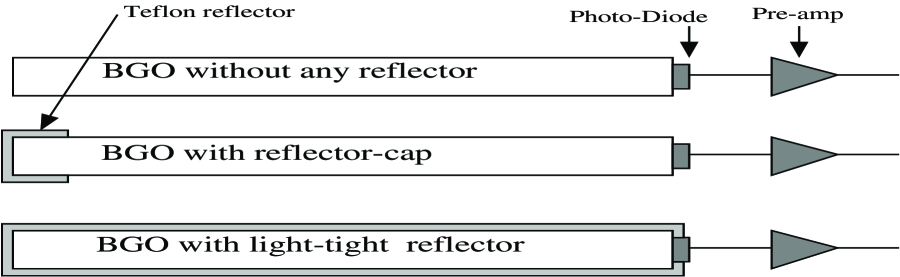
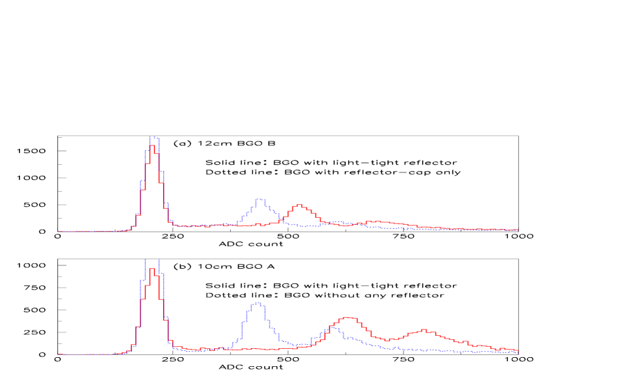
Effect of reflector : We also studied the advantage of the teflon reflector around the crystal. BGO has a high refractive index of 2.15, and therefore is supposed to retain most of the scintillation light by total internal reflection. We did the following experiment in order to study the effect of putting on a teflon reflector around the crystals. First, we stripped the reflector off the sample B except for the very end opposite to the photodiode(we will call this setup as “BGO with a reflector-cap”). Then the sample was subjected to the 3.5 GeV beam. The pulse height spectrum is given in Fig. 5(a) as the solid line. Then we removed the reflector completely, leaving the crystal bare. It was then subjected to the beam, and the observed pulse-height spectrum is shown in Fig. 5(a) as the dotted line.
We can easily distinguish the MIP and nuclear counter peaks in these two superimposed plots. It can be readily seen by comparing the position of the two MIP peaks after pedestal subtraction, that a reflector cap increases the light collection in BGO by about 30% compared to a bare crystal.
We then took the sample A, completely wrapped with the reflector, and subjected it to the beam. The ADC spectrum is plotted in Fig. 5(b) as the solid line. Then we stripped the reflector completely off the sample, and repeated the experiment. The corresponding ADC spectrum is plotted as the dotted line in Fig. 5(b).
Again, the peaks due to the MIP and NCE are clearly visible. By comparing the two MIP peaks after pedestal subtraction, it can be seen that the light collection with full reflector wrap improves by about 85% compared to the bare crystal.
It is interesting to note that (Fig. 5) the height of the NCE peak with respect to the MIP peak is smaller for sample B compared to that for sample A. The reason may be ascribed to the larger length of sample B, where more scintillation light is collected by the PD, thereby pulling down the ratio.
5 Summary
-
•
BGO and BSO crystals coupled with photodiodes are proven to be capable of detecting minimum-ionizing particles with a large S/N ratio. The preamplifier used is perfectly adequate for the purpose. The signal of MIPs is well separated from electronic noise and NCE signal.
-
•
The detection of MIPs with BSO coupled with a PD is reported for the first time.
-
•
A clear effect of NCE in a calorimetric environment is reported for the first time.
-
•
Effect of reflector wrap around the crystal in regards to the light collection is studied.
Acknowledgements
The MIP detection experiment was done under the auspices of National Lab for High Energy Physics (KEK) as the experiment T-388 of the KEK-PS. We would like to thank Dr. M. Kobayashi for providing valuable information on BSO, and Dr. Y. Sugimoto for valuable suggestions on preamps. The Aerogel and CsI subgroup members of the BELLE collaboration have been extremely helpful in this project. This experiment was supported in part by the grant NSC 85-2112-M-002-034 of the Republic of China.
References
- [1] R. Sumner et al., Nucl. Instr. Meth. A265(1988)252.
- [2] H. Hayashii et al., Nucl. Instr. Meth. A316(1992)202.
- [3] D.N. Grigoriev et al., IEEE Tran. Nucl. Scie. 42(1995)505.
- [4] M. Kobayashi et al., Nucl. Instr. Meth. A372(1996)45.
- [5] V.V. Yanovskii et al., Nucl. Instr. Meth. A309(1991)596.
- [6] S.K. Sahu et al., KEK Preprint 96-148, to be published in Nucl. Instr. Meth. A.
- [7] Proceedings of the Workshop on Backgrounds at the Machine Detector Interface(1995), UH-511-838-96 (Ed. T.E. Browder), Department of Physics & Astronomy, Univ. of Hawaii, 2505 Correa Rd., Honolulu, HI 96822, USA.
- [8] BELLE Progress Report, KEK Progress Report 95-1 H.
- [9] W.S. Hou et al., BELLE Note 90(1995).
- [10] Y. Sugimoto et al., KEK Preprint 96-126, to be published in Nucl. Instr. Meth. A.
- [11] Hamamatsu Photonics K.K., 325-6 Sunayama, Hamamatsu 430, Japan.
- [12] Institute of Inorganic Chemistry, Ak. Lavrentyev 3, Novosibirsk 630090, Russia.
- [13] Institute for Single Crystals, 60 Lenin Ave., 310001 Kharkov, Ukraine.
- [14] Futec Furnace Co., 2-7-33 Fukuura, Kanazawa-ku, Yokohama 236, Japan.
- [15] Eccobond-24; From GRACE Japan inc., 2-16-10 Shibuya-ku Higashi, Tokyo 150, Japan.; H.C. Huang et al., Nucl. Instr. Meth. A385(1997)559.
- [16] CERN Program Library Long Writeup W5013.
Table Captions
Tab. 1 : Peak channels and widths for Fig. 2, see text for details.
Figure Captions
Fig. 1 : Circuit diagram of the charge preamplifier. Shaping time is about 1 s.
Fig. 2 : Study of the charge preamplifier : (a) Response of preamp to a test pulse. The charge-amp gain is measured to be 6.2 V/pC; (b) Response of PD(S5106) + preamp with JFET(715) to 60 keV -rays from 241Am. ENC is 548 electrons; (c) Same configuration as (b), but with a larger PD(S2662-03). ENC is 970 electrons; (d) Same configuration as (c) but JFET switched to 2SK291. ENC is 906 electrons.
Fig. 3 : Setup for the MIP detection experiment.
Fig. 4 : Observation of MIP signal with 3.5 GeV beam : (a) Observed ADC counts for 10 cm long BGO sample A. Solid line is the real data, and dashed line is simulated data(not normalized with real data). (b) Observed ADC counts for 12 cm long BGO sample B. (c) Observed ADC counts for 12 cm long BSO sample C. (d) Observed ADC counts for MIP hitting PD directly in the absence of any crystal.
Fig. 5 : Study of the effect of Teflon reflector on light collection : In the top, the three configurations are sketched, and referred to in the plots. (a) Observed ADC counts for sample B, with complete reflector and with partial reflector. (b) Observed ADC counts for sample A, with complete reflector and with no reflector.
| Condition | Signal Peak | Gaussian | Pedestal | |||
|---|---|---|---|---|---|---|
| Test Pulse | 1038. | .04 | 7.6 | .04 | 24.4 | .03 |
| Small PD(S5106) + JFET(715) | 507.5 | .1 | 15.9 | .2 | 23.5 | .06 |
| Large PD(S2662-03) + JFET(715) | 489.3 | .3 | 27.2 | .3 | 22.0 | .2 |
| Large PD(S2662-03) + JFET(291) | 459.0 | .2 | 23.8 | .3 | 21.2 | .2 |
Figure 1, K. Ueno et al., NIM-A

Figure 2, K. Ueno et al., NIM-A

Figure 3, K. Ueno et al., NIM-A
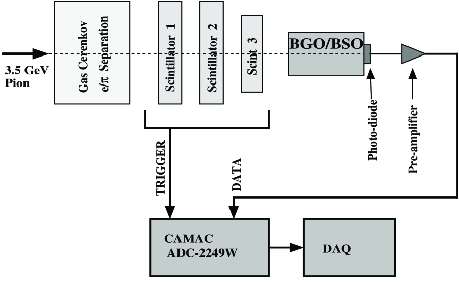
Figure 4, K. Ueno et al., NIM-A
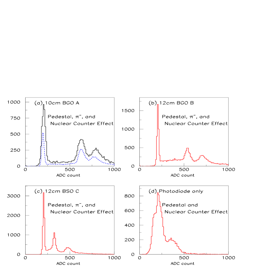
Figure 5, K. Ueno et al., NIM-A