Design and performance of the silicon sensors
for the CMS barrel pixel detector
Abstract
The CMS experiment at the LHC includes a hybrid silicon pixel detector for the reconstruction of charged tracks and of the interaction vertices. The barrel region consists of n-in-n sensors with m2 cell size processed on diffusion oxygenated float zone silicon. A biasing grid is implemented and pixel isolation is achieved with the moderated p-spray technique. An extensive test program was carried out on the H2 beam line of the CERN SPS. In this paper we describe the sensor layout, the beam test setup and the results obtained with both irradiated and non-irradiated prototype devices. Measurements of charge collection, hit detection efficiency, Lorentz angle and spatial resolution are presented.
, , , , , , ,, , , , , , , , , , ,
1 Introduction
The CMS experiment, currently under construction at the Large Hadron Collider (LHC) will include a silicon pixel detector [1] to allow tracking in the region closest to the interaction point. The detector will be a key component for reconstructing interaction vertices and heavy quark decays in a particularly harsh environment, characterized by a high track multiplicity and heavy irradiation. The detector will consist of three barrel layers and two disks at each end of the barrel. The innermost barrel layer has a radius of 4.3 cm, while for the second and third layers the radius is of 7.2 cm and 11 cm, respectively. The layers are composed of modular detector units. These modules consist of thin, segmented silicon sensors with highly integrated readout chips connected by the bump bonding technique. They are attached to cooling frames, the cooling tubes being an integral part of the mechanical structure. The minimal pixel size is dictated by the readout circuit area required for each pixel. In finding and localizing secondary decay vertices both transverse () and longitudinal () coordinates are important in the barrel region. Therefore a nearly square pixel shape is preferred. Because charge is often shared among several pixels, the use of analogue signal readout enables position interpolation improving the spatial resolution. In the barrel the charge sharing in the -direction will be large due to the 4 T magnetic field of CMS. With a sensitive detector thickness of 285 m the pixel size will be 100 m and 150 m along the and coordinates, respectively. These value will give favourable spatial resolution and cluster sizes.
One of the greatest challenges in the design of the pixel detector is the high radiation level on all components at very close distances to the colliding beams. At full LHC luminosity the innermost layer will be exposed to a particle fluence of ncm2/yr 111All fluences are normalized to the non-ionizing energy loss (NIEL) of 1 MeV neutrons (ncm2)., the second and third layer to about ncm2/yr and ncm2/yr, respectively. All components of the pixel system are specified to stay operational up to a particle fluence of at least ncm2. This implies that parts of the detector will have to be replaced during the lifetime of the experiment. In case of a possible luminosity upgrade of the LHC the particle fluence will be even higher. For this reason it is necessary to test whether the detectors can be operated at fluences above the ones specified above.
Particle irradiation affects the silicon sensor response in various ways. It is common practice to divide radiation damage into surface and bulk damages. The former includes all effects caused by ionization in the dielectric covering the structured sensor surface. Most important is the increase of charge in the silicon oxide which saturates after some kGy to values of a few cm-2. This changes the electric field close to the collecting electrodes and may lead to electric breakdown. At higher particle fluences bulk damage, caused by the interaction of the incident particles with the silicon lattice atoms, also becomes important. Silicon atoms can be ejected from their lattice sites leaving vacancies, and the recoil atoms can collide with other lattice atoms. With large enough recoil energy other atoms are displaced, creating more vacancies and interstitials (also called Frenkel pairs or primary defects). The thermal energy of the crystal enables some of the simple defects and defect clusters to migrate through the lattice and to react with other defects or impurities (e.g. dopants such as phosphorous and boron or crystal impurities such as oxygen and carbon). The formation of complex defects produces new energy states in the band gap, some of which can be electrically charged.
There are mainly three macroscopic manifestations of the defects in reverse biased silicon detectors: An increase of the leakage current, the modification of the space charge density and of the drift field across the bulk, and the trapping of charge carriers.
The increase of leakage current leads to a higher power dissipation and to a rise of the sensor temperature. Proper cooling is required to prevent a destructive “thermal runaway” of the device. As the pixel current is still very small the noise increase is not critical. However, the preamplifier DC-coupled to each pixel must be able to drain the excess of leakage current. The formation and annealing of the crystal defects show a complex time behaviour which is strongly temperature dependent. It is advantageous to keep the sensors cooled to about -10∘C not only during operation but also during shutdown periods to inhibit reverse annealing. In addition, it was shown that radiation tolerance can be improved by enriching the starting material with oxygen [2].
Trapping of the mobile carriers from the leakage current produces a net positive space charge density near the p+-backplane and a net negative space charge density near the n+-implant. Since positive space charge density corresponds to n-type doping and negative space charge corresponds to p-type doping, there are p-n junctions at both sides of the detector. Consequently, the electric field profile across the bulk varies with an approximately quadratic dependence having a minimum at the zero of the space charge density and maxima at both implants [3, 4, 5, 6, 7, 8, 9, 10]. The energy levels associated with the crystal defects are not only filled by charge carriers from the generation-recombination current (leakage current) but also by carriers produced by traversing particles. If these carriers are trapped for a time longer than the signal collection time they do not contribute to particle detection and are de facto lost. Trapping can be reduced by collecting electrons instead of holes, because they have a higher mobility and are less prone to trapping. In addition, high drift fields and fast signal collection can be achieved by increasing the bias voltage. Signal reduction caused by trapping presently limits the use of silicon detectors in environments exposed to fluences higher than 1015 ncm2.
The optimization of the CMS barrel pixel sensors was achieved through an extensive comparison of several technological choices [11, 12, 13, 14, 15, 16]. In particular, pixel sensors with p-spray and p-stop isolation of the collecting electrodes were compared and the p-spray technique was chosen for the barrel design [16]. Therefore, only the results obtained with pixel sensors implementing a p-spray isolation are discussed hereafter. The purpose of the beam test program described in this paper was to investigate several aspects of the sensors response:
-
•
Prove that after a given irradiation fluence the bias voltage could be adjusted to collect sufficient charge. In addition, due to the sparsified readout, sensor regions with lower charge collection can lead to detection inefficiencies which may be reduced by design optimization.
-
•
A good spatial resolution must be guaranteed during operation. In the CMS transverse plane most tracks are perpendicular to the sensors and charge is distributed among several pixels by the Lorentz deflection which is affected both by the applied bias voltage and by irradiation. Along the longitudinal direction larger impact angles produce clusters of several pixels and the unhomogeneous charge collection caused by trapping produces asymmetric clusters. Thus, appropriate hit reconstruction techniques have to be developed to maximize precision.
This paper presents a detailed description of the sensors for the CMS barrel pixel detector and their performance. Emphasis is put on highly irradiated sensors. The paper is structured as follows: A detailed description of the pixel sensors layout is given in Section 2. Both the final and prototype sensors used for the tests are discussed. The samples used for the beam tests are described in Section 3 and the electrical measurements are presented in Section 4. The setup developed for the beam tests is described in Section 5 and the data reduction discussed in Section 6. The results of the beam test measurements are presented is Section 7. Conclusions are presented in Section 8.
2 Sensor Description
2.1 Sensor dimensions and geometry
For the CMS barrel pixel detector two different sensor geometries, the so-called full and half modules are required. The full modules house readout chips. The half modules have only readout chips. Each readout chip contains pixels with dimensions of m2 [1].
For the beam test measurements presented in this paper a special readout chip with pixels of m2 was used. Special sensors were designed to match the chip dimensions. The pixel cell was scaled keeping the gap between the implants constant in order not to change the charge collection properties of the sensor. All other design features were kept identical to the final sensors. Therefore it is not expected that the basic properties other than the spatial resolution differ significantly from the final barrel sensor design.
2.2 Technological choices
The sensors for the CMS pixel detector adopt the so called “n-in-n” concept: Pixels consist of high dose n-implants introduced into a highly resistive n-substrate. The backside of the substrate is p-doped, therefore the pn-junction is placed on the backside of the sensor. As the junction must not extend to the diced edge of the sensor a structured back side and, consequently, a double-sided processing of the wafers is mandatory. Additional precautions have to be taken to suppress the electron accumulation layer shortening the pixels on the front side of the sensor. Both considerations lead to a significant cost increase compared to the single sided “p-in-n” sensors widely used for strip detectors. However, this concept was chosen for the following reasons:
-
•
It assures a high signal charge at moderated bias voltages (V) after high hadron fluences (see Sect. 7.4);
-
•
The high mobility of electrons leads to a larger Lorentz angle, important to reach the required spatial resolution;
-
•
The need to structure the back side allows to implement a guard ring scheme keeping all sensor edges at ground potential.
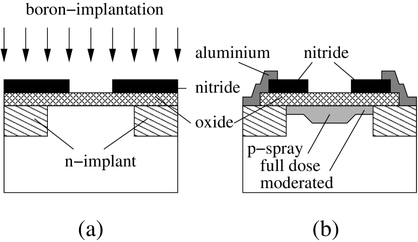
Two inter-pixel isolation techniques were evaluated for the barrel sensors: Open p-stops [17] and moderated p-spray [18]. The moderated p-spray technique was eventually chosen because of the superior charge collection properties obtained with the prototype sensors [19]. The p-spray consists of a medium dose boron implantation “sprayed” without mask over the whole wafer. Due to the topology on the wafer surface, the implant is “moderated” in the region of the lateral pn-junction between pixel implant and the isolation, as sketched in Fig. 2. The implantation parameters are adjusted in a way that in the moderated region the boron dose matches as close as possible the expected saturation value of the oxide charge, reached after a few kGy of ionising radiation. Far from the lateral pn-junction the boron dose reaching the silicon can be roughly 2-3 times larger. This improves the high voltage stability of the unirradiated devices compared to a “non-moderated” p-spray [20] while keeping the good post-radiation behaviour.
As ground material n-doped FZ-silicon with orientation and a resistivity of cm was used. All wafers for the production of the barrel sensors come from the same silicon ingot to provide the best possible homogeneity of all material parameters. To improve the post radiation behaviour the wafers undergo a oxygen diffusion process as recommended by the ROSE collaboration [21] resulting in the so-called DOFZ-material.
2.3 Mask layout
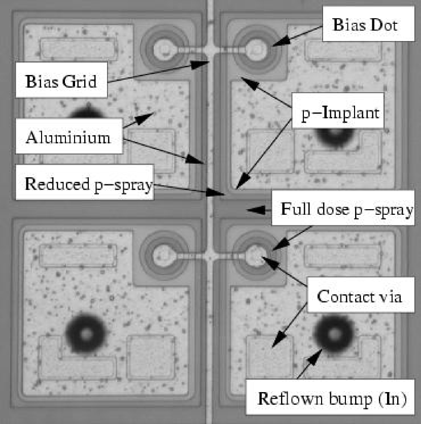
A photograph of four pixels is shown in Fig. 1. The pixel size was in this case defined by the choice of the readout chip for the test beam. While the CMS detector will be equipped with pixels of m length along the beam pipe and m width in the polar direction, the tested prototypes had dimensions of m2.
Most of the pixel area is covered with the collecting electrode formed by the n-implant. The gap between the n-implants is kept rather small (m) to provide a homogeneous drift field for the signal charge. On the other hand, this small gap leads to a relatively high capacitance of the order of 80-100 fF per pixel which is still compatible with noise requirements. In order to reduce electric field peaks the corners of the implant are rounded.
The so-called bias dot is visible in one corner of each pixel (Fig. 1). It consists of a circular n-implant isolated from the pixel implant by a small gap. It is connected through a contact via to a circular metal pad. These pads are routed to a metal line running along every second pixel column. They form a bias grid which provides a high resistive punch-through connection to all pixels. The grid allows on-wafer current-voltage (IV) measurements prior to bump bonding which are performed to detect faulty sensors. In the assembled module the pixels are grounded by the bump bond connection to the preamplifier (DC-coupling) and the grid is used to bias accidentally unconnected pixels.
The dark “frame” around the pixel implants visible in Fig. 2 indicates the opening in the nitride covering the thermal oxide. In this region the p-spray dose reaches its maximum. The boron dose is reduced close to the lateral pn-junction between the pixel implant and the p-sprayed inter-pixel region. To increase the punch through voltage the full p-spray dose is applied between the bias dot and the pixel implant. This is possible as the gap is small compared to the gap between the pixels and both gaps are electrically isolated from each other another.
The pixel metalization is slightly smaller than the pixel implant. An overhanging field plate could not be implemented as the metal connection of the bias grid had to cross the edge of the pixel implant. The metalisation is connected to the underlying implant via several contact holes. Since too large openings might reduce the production yield, their total area was kept small.
The sensor shown in Fig. 1 has undergone the bump deposition process including the reflow of the bumps. The bumps are Indium droplets approximately 25 m in diameter. Due to their finite size they are out of the focus of the microscope.
The active area of the module is surrounded by a m wide n-implanted ring to which all metal lines from the bias grid are connected. This bias ring can be contacted either by large wire bond pads in the sensor corner or via a special bump pad on the readout chip, although this is currently not foreseen. The region outside this structure spans a large area n-implant up to the scribe line. It will be connected to the analogue ground of the readout chip via a second special bump pad. This connection ensures that the whole sensor edge is kept at ground potential and in addition drains the current from the guard ring region. In the test samples investigated during this study this connection was open and the outer region was floating. The edge current was therefore not drained but equally distributed over all pixels via the bias grid. However, the noise increase produced by the extra current flowing into the preamplifier was negligible.
The back side of the sensor consists of a large p-implant forming the junction that depletes the sensor. This p-implant overlaps the sensitive region by m to provide a homogeneous drift field also in the edge pixels. The metalization is open in almost the whole sensitive area apart from the wire bond pad for the bias voltage, as visible in Fig. 3. This allows charge injection by a laser.
The sensor is surrounded by a multiguard ring structure, shown in Fig. 3, that guarantees a gradual potential drop to the scribe line and prevents the lateral extension of the space charge region. It consists on 16 p-implanted guard rings with a distance increasing from m in the innermost ring to m in the outermost. The aluminisation of the rings is overhanging in both directions. A small metal overlap directed toward the scribe line reduces the electric field at the implant edge. A larger overlap toward the device centre increases the voltage drop between rings [22, 23].
3 Sample preparation
The single chip sensors used in the test beam measurements (Section 7) were produced in 2002 by CiS, Erfurt, Germany. The deposition of the under bump metalisation (UBM) and the indium bumps on wafer was performed at PSI. Then the wafers were diced and the bumps reflown. Some of the sensors were bump bonded to the readout chips and glued to support cards.
The treatment of irradiated sensors is more complex. Sensors were irradiated before bump bonding. This was required to study the effects of irradiation on sensors only. In addition, the readout chip used for this study was not sufficiently radiation hard. The bump deposition and reflow involve temperatures above C. To prevent reverse annealing these steps had to be performed before irradiation.
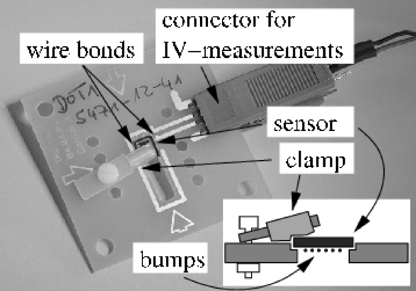
For irradiation the diced sensors were mounted on the PCBs shown in Fig. 4. These mm2 PCBs can safely be transported in slide holders, thus the fragile bumps are protected. The wire bond connection to the sensor’s back side easily allows IV-measurements.
The irradiation has been carried out in 2003 and 2004 at the CERN-PS using 21-24 GeV protons. The delivered proton fluences scaled to 1 MeV neutrons by the hardness factor 0.62 [21] were between and . The irradiation was performed without cooling and no bias applied. After irradiation the samples were stored in a freezer at C and warmed up to room temperature only for handling and transport.
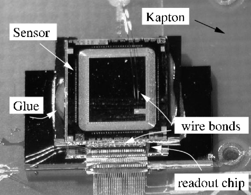
For mating the sensor to the readout chip a special procedure without heat treatment was developed. The mechanical strength of the bump bond connections usually obtained after a second reflow was achieved by the application of glue (see Fig. 3). The assembly was then attached to a Kapton card an the electrical connections were established by wire bonds. The Kapton cards can be inserted into the cooled rotating stage of the beam telescope (see Fig. 6 below).
After final assembly the samples underwent annealing of three days at C. This was done to adjust the depletion voltage close to its minimum according to the Hamburg model for DOFZ material [21].
4 Electrical measurements
To assure that the samples were not mechanically damaged during the long and complex preparation, IV-characteristics were measured before each important assembly step:
-
1.
Shortly before irradiation, after mounting and wire bonding the sample to the support structure.
-
2.
A few days after irradiation, when the sample was still mounted on the support card.
-
3.
After bump bonding and mounting on the Kapton card.
-
4.
During the beam test.
Sensors with obvious damage leading to low breakdown voltage or extremely high leakage current were excluded from further assembly. The IV-curves of the sensors used for the measurements discussed in Section 7 are shown in Fig. 5. The current is normalized to C using the temperature dependence of the volume generation current:
| (1) |
where is the absolute temperature, the band gap in silicon and the Boltzmann constant. The temperature was measured using a platinum thermistor (PT100) located close to the sensor. The error bands visible in Fig. 5 are due to the uncertainty on the temperature, which was estimated to C for the measurement of the unirradiated sensor and the data extracted from the test beam slow control system and C for the other measurements. The temperature difference between the pixel sensor and the thermistor for bump bonded devices was estimated by comparing the sensor leakage current with and without power applied to the frontend chip.
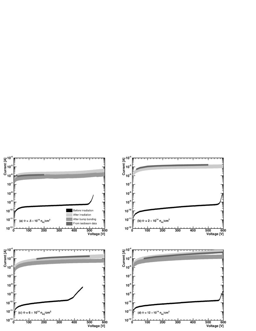
The expected leakage current [24] is in the lower part of the error bands. A factor of about two can be explained by the extremely large edge area of the small sensors (the guard current is not drained separately). The high mechanical stress caused by the special bump bonding process involving glue application may also leads to a current increase.
More important than the level of the leakage current is the shape of the IV-curve. While the unirradiated sensors show a breakdown voltage between 400 V and 600 V, no breakdown is observed after irradiation. This proves the high radiation tolerance of the moderated p-spray technique used for these devices.
5 Beam test setup
The measurements were performed in the H2 beam line of the CERN SPS in 2003-04 using 150-225 GeV pions. The test setup was placed in an open-geometry 3 T Helmoltz magnet producing a magnetic field parallel or perpendicular to the beam.
5.1 Beam telescope
A silicon reference telescope [25] was used to allow a precise determination of the particle hit coordinates in the pixel detector (see Figure 6). The telescope modules and the hybrid pixel detector were mounted on a common frame. The beam telescope consisted of four modules, each including two orthogonal 300 m thick single-sided silicon strip detectors to measure the horizontal and vertical impact coordinates. The sensors have a strip pitch of 25 m, a readout pitch of 50 m and a total sensitive surface of mm2. The intrinsic position resolution of the beam telescope is about 1 m [25].
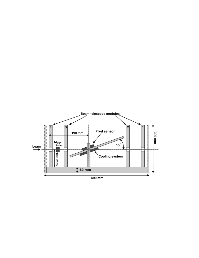
The pixel hybrid detector and the readout card are mounted between the second and third telescope module on a cooled rotating stage. The rotation is around the horizontal axis and a precision of 0.2∘ is achieved. A trigger signal is generated by a silicon PIN diode placed between the first and second telescope modules. The horizontal and vertical positions of the diode can be adjusted with a precision of about 100 m.
5.2 Pixel sensors assembly and cooling
The hybrid pixel sensor is enclosed in a thermo–isolated plastic box flushed with dry nitrogen to avoid water condensation. The readout chip is bump-bonded to the pixel sensor and glued to a printed circuit board (PCB). The pixel readout card is connected to the PCB via a short flat cable.
The power consumption of the pixel readout chip and the readout card is about 20 W. This heat has to be efficiently removed by the cooling system. Therefore, two high performance Peltier elements attached to a liquid cooled heat sink are used to chill the sensor. The hot ceramic side of the Peltier elements is in direct contact with the coolant liquid, which is circulated by an external Lauda WKL600 chiller.
The temperature is measured with a PT1000 platinum resistor placed on the PCB and stabilized by regulating the voltage applied to the Peltier elements. Heat conducting paste is used to improve the thermal contact between the cold aluminum plates and the PCB. The sensor resistance is measured with a Keithley 2000 multimeter and the temperature can be stabilized down to -35∘ C.
5.3 Sensors readout and data acquisition
A schematic view of the readout is shown in Fig. 7. The analog signals of the 2232 pixels are read out by the PSI30/AC30 readout chip [26]. Each pixel cell is read out by a preamplifier and a shaper with a peaking time adjusted to 45 ns.The readout is enabled when the particle crosses the PIN diode area and a trigger pulse is sent to the sample–and–hold (S/H) input of the readout chip. The active level of the S/H signal disconnects a capacitor attached to the shaper output and the signal amplitude is stored in the capacitor. In addition, the signal discrimination is disabled to allow the readout of all cells. The analog amplitudes are digitized by a 12 bits 40 MHz ADC.
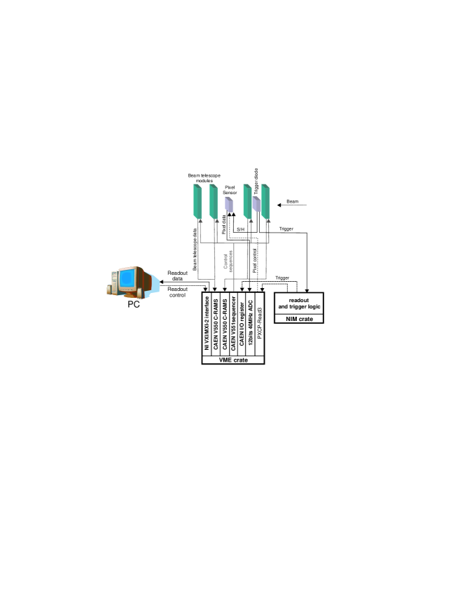
The trigger signal is also used to start the readout of the beam telescope modules. The charge collected by the strip sensors is amplified and integrated in a time window of about 2 s. The signals are then digitized by two CAEN V550 units controlled by a CAEN V551 sequencer.
The data acquisition (DAQ) software is written in LabView and LabWindows CVI222LabView and LabWindows/CVI are products of National Instruments. and runs on a PC. It controls the VME crate via a National Instruments PCI interface, the power supplies for the pixel sensor and the Peltier elements, and the multimeter for the temperature measurements.
The pixel settings and trigger types can be changed. The telescope, pixel signal amplitudes and pedestal values are stored in a data file. Each event is marked with a time stamp and the values of the pixel bias voltage, dark current and temperature are recorded.
6 Data analysis
6.1 Event selection
The channel noise and pedestal levels are measured with dedicated random trigger runs taken during the spill gaps. The signal amplitudes of each pixel cell is reconstructed with the following procedure [27]:
-
1.
Pixel pedestals stored in the data file are subtracted from the amplitudes cell by cell.
-
2.
The amplitudes of six unconnected pixel rows are averaged and subtracted to reduce common mode fluctuation.
-
3.
Hit pixels above threshold (which depends on the irradiation fluence), are further analyzed. The threshold is optimized for each sample and ranges between 35 – 50 ADC counts (corresponding to 1000 – 1500 electrons).
-
4.
If the hit frequency is below 0.1 times or above 10 times the expected one, the pixel is marked as noisy or dead and excluded from the amplitude reconstruction.
-
5.
Improved pedestals and common mode values derived from the good pixels with amplitudes below threshold, are calculated and subtracted from the pixel amplitudes.
Steps (iii), (iv) and (v) are repeated for four iterations. The signal amplitudes of the telescope strip sensors are reconstructed and corrected in a similar way.
Events used for the alignment of the pixel detector with the beam telescope are selected. The selection procedure discards the events with multiple tracks and tracks which do not fit to straight lines.
6.2 Alignment of the pixel sensor with the beam telescope
In each beam telescope plane the position of the impact point is reconstructed with a center of gravity algorithm for clusters of two adjacent strips. The main strip in the cluster must have a signal between 30 and 350 ADC counts and the second strip is the next neighbour with the highest amplitude. The hit position is then corrected using the algorithm described in [28].
The determination of the particle impact position in the pixel sensor depends on the track incident angle with respect to the pixel plane (see Fig. 8). For the hit position is measured using a center of gravity algorithm. The pixel with the highest signal above threshold is located and the surrounding eight pixels are included in the cluster. The cluster is projected along the two coordinates and . The weighted averages of the hit coordinates and are calculated.
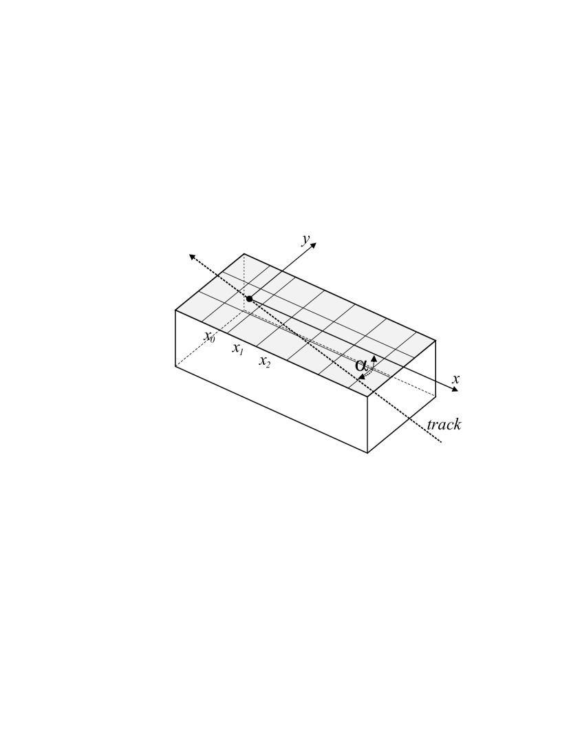
For small angles, e.g. , the cluster size along is in general larger than three pixels and a different approach is used. The pixel corresponding to the track exit point is defined by the first pixel above threshold along the axis and with the highest signal along the axis. A cluster is constructed by including the following two pixels along the axis, which are required to be over threshold, and the corresponding three pixels in the upper and lower rows along the axis. The coordinate of the cluster is determined with the center of gravity of the signal collected in the three -rows. The coordinate of the track exit point is determined using the signal in the three cluster -columns. We define the signals and the coordinates of the three pixel columns, respectively. The signal sums with vs. their coordinates are fitted with a straight line. The intercept of this line with the axis gives the coordinate of the track exit point.
The alignment is performed by minimizing the residuals in the following system of equations
| (2) | |||||
| (3) |
where is the position in the -th beam telescope plane333The indexes correspond to the position in the planes, while to the positions in telescope planes. for the -th event, and are the hit coordinates in the pixel coordinate system, and are the residuals in the and coordinates, respectively, and are the fit parameters for the and coordinates, respectively.
6.3 Gain calibration
A calibration of the readout chain can be performed by injecting a known charge at the input of the chip preamplifier via a 1.7 pF capacitor. The average signal as a function of the time interval between the calibration and the trigger pulses is show in Fig. 9. The average signal measured with straight minimum ionizing tracks and an unirradiated sensor is 710 ADC counts. This implies that the sampling time of our measurements is about 55 ns.
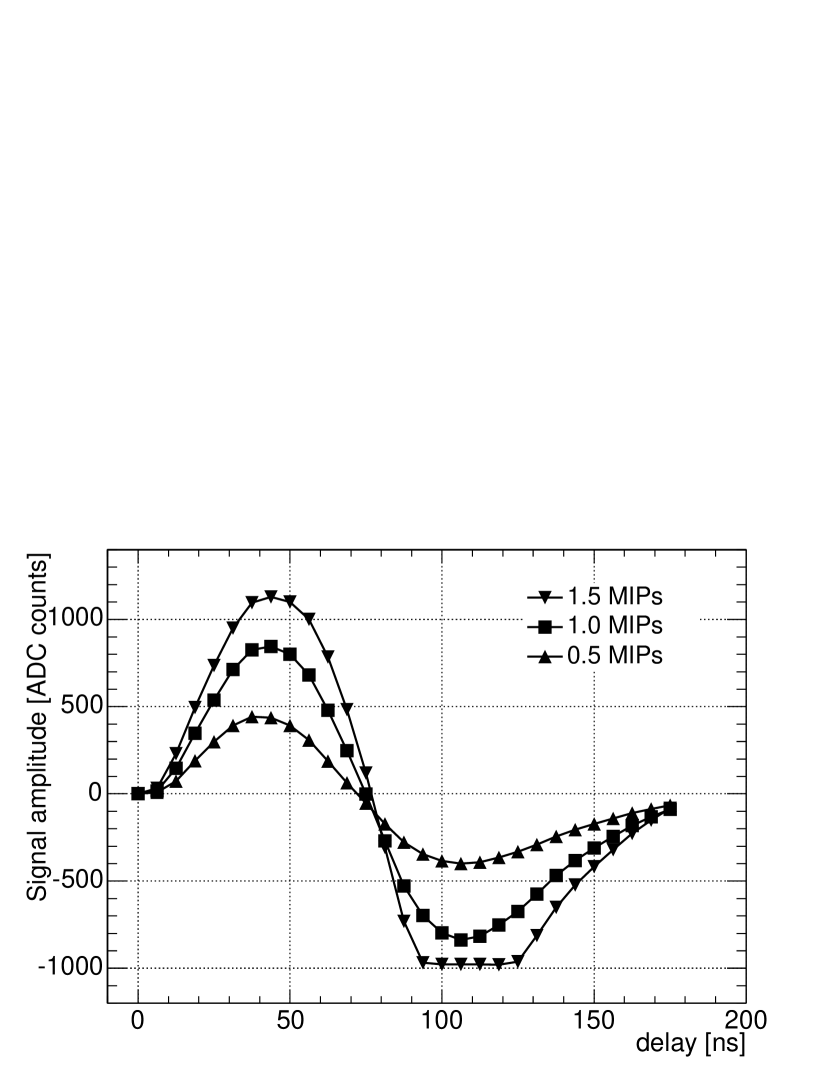
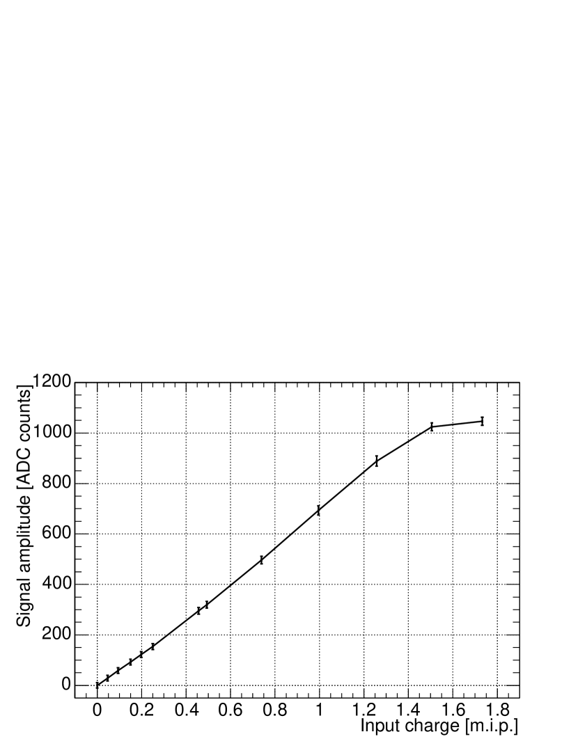
The gain calibration is performed by setting the delay to this value and measuring the average signal amplitude as function of the charge injected in the preamplifier (see Fig. 9). The charge released by a minimum ionizing particle (m.i.p.) is 22400 electrons for a silicon thickness of 285 m. The response of the frontend electronics is fairly linear up to about 1.2 m.i.p. and saturates for higher values of the injected charge. Figure 9 is used hereafter to translate the ADC values into charge in electrons. More details about the gain calibration can be found in [27].
7 Results
7.1 Signal-over-noise ratio
Signal, noise and their ratio measured after different irradiation fluences and bias voltages are summarized in Table 1. The signal was defined as the average signal recorded by the hit pixel with tracks perpendicular to the sensor plane, while noise was the r.m.s of a Gaussian fit applied to the signal distribution recorded between spill gaps. The measurements were performed with tracks perpendicular to the sensor surface without magnetic field. As discussed above, the bias voltage must be increased after irradiation in order to collect charge from the full sensor thickness. The optimal bias voltage at each fluence was set to the minimum value at which charge collection saturates, as discussed in Section 7.4.
| Fluence | Bias voltage | Signal | Noise | S/N ratio |
|---|---|---|---|---|
| ] | [V] | [ADC counts] | [ADC counts] | |
| 0 | 150 | 727.7 | 11.1 | 65.2 |
| 150 | 633.2 | 8.9 | 70.9 | |
| 200 | 654.0 | 10.9 | 59.8 | |
| 400 | 475.6 | 9.9 | 48.2 | |
| 600 | 430.5 | 22.8 | 18.9 | |
| 600 | 198.0 | 19.5 | 10.1 |
The measured signal over noise ratio is high even after high fluences.
At a fluence of ,
roughly corresponding to the first four years of LHC operation of the innermost layer,
it exceeds 40 which corresponds to a charge of 15500 electrons, roughly
65% of the value measured with the unirradiated sensor.
By doubling the irradiation fluence the signal drops to 59% of the unirradiated
sensor signal when the bias voltage is increased to 600 V. The noise becomes
quite high and the signal over noise ratio decreases to about 20.
The high noise is partly caused by the absence of leakage current compensation
in the readout chip.
Nevertheless, as we show in Section 7.3, it is still
possible to operate the sensor with a charge threshold of 2000 electrons maintaining
the hit detection efficiency above 97%.
The most irradiated sample is a factor of four above specifications and almost
in the range of irradiation fluences expected after LHC upgrade.
The average signal is then about 6300 electrons. For efficient
particle detection the threshold has to be set below 3000 electrons and
the noise level kept below 600 electrons. This might be possible with
a readout chip implementing a well–suited leakage current compensation.
7.2 Position dependence of charge collection
The structured surface of the sensor can lead to spatial variations in charge collection. We have therefore investigated the charge collection with tracks perpendicular to the sensor plane without magnetic field.
Figure 10 shows the average collected charge as a function of the hit position predicted by the beam telescope for an unirradiated sensor operated at 150 V (Fig. 10 and (b)) and a sensor irradiated to a fluence of ncm2 and operated at 450 V (Fig. 10 and (d)). Shown are four pixel cells with the metal line along the vertical axis at the m position. The left column (Fig. 10 and (c)) shows the charge collected in the hit pixel while the right column (Fig. 10 and (d)) shows the charge in a cluster around the hit pixel.
In the unirradiated sensor the charge is uniformly collected within the pixel implant with the exception of the punch-through biasing structure where the signal is reduced by up to 50%. The latter is located too far from the pixel edge so that the charge deposited in this position is not shared with other pixels. The effect of the punch-through structure on the overall sensor performance is very limited as it represents only 2–3% of the total surface.
In the region between pixel implants the charge summed over a cluster is not noticeably affected (see Fig. 10). Charge sharing is restricted to a region of about 10 m around the pixel edge, where the signal in the hit pixel decreases. It will be enhanced by the external 4 T magnetic field of CMS and also for non perpendicular tracks.
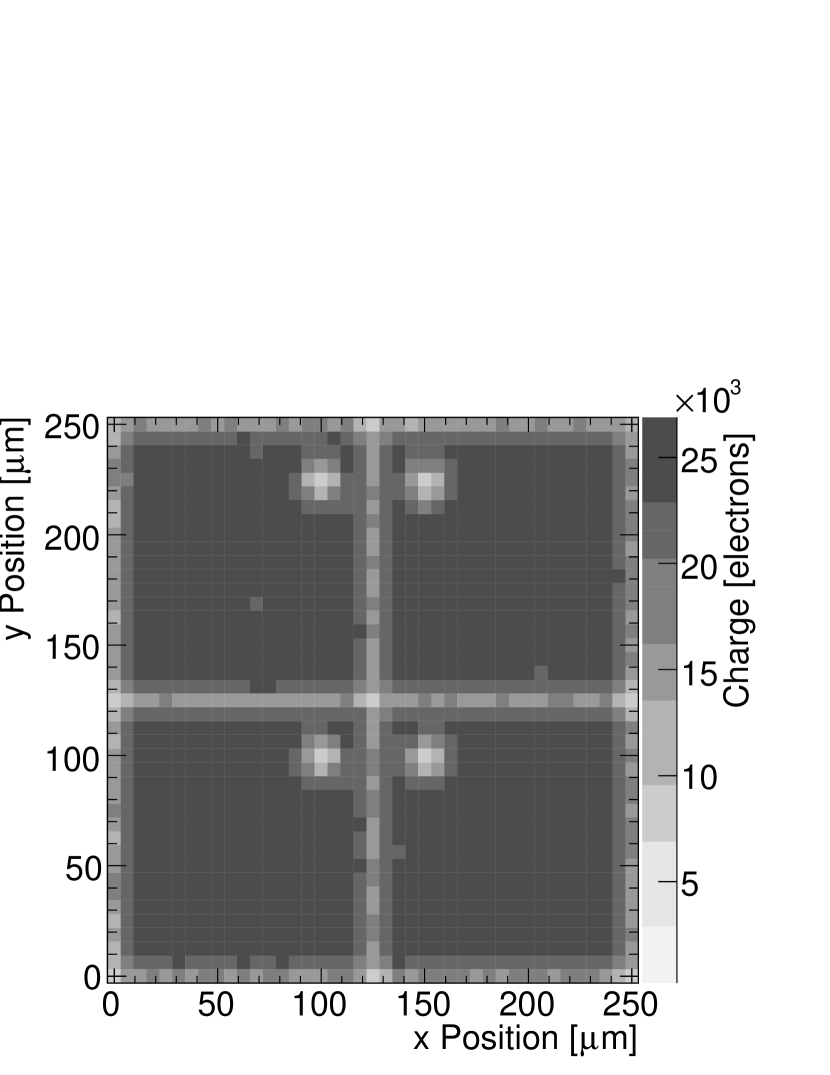
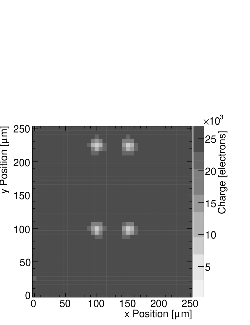

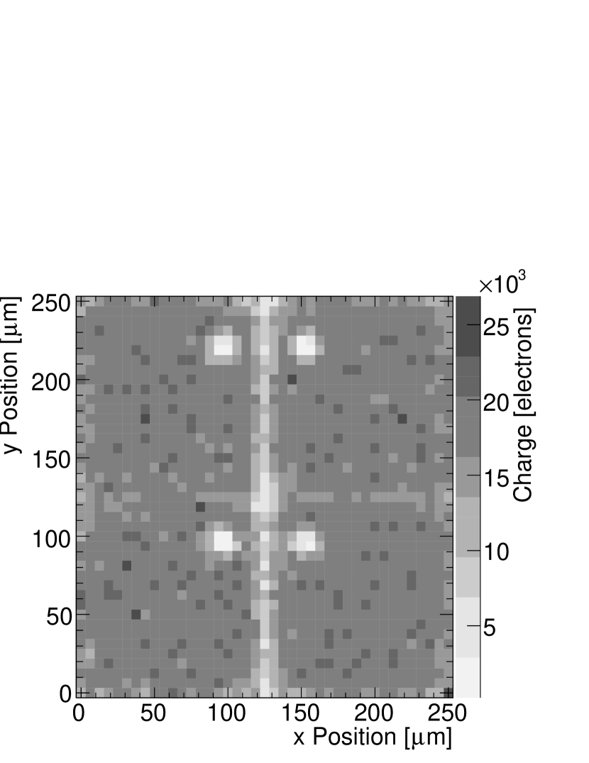
After irradiation the charge collected in the hit pixel decreases by about 30% due to trapping of the charge carriers and the charge losses in the punch-through structures become more prominent. The sum of the charge collected in the hit pixel and in the surrounding neighbours is shown in Fig. 10. Charge sharing is uniform after irradiation along all pixel borders except for the region around the metal line. Similar effects were observed with other hybrid pixel detectors implementing a biasing grid [29] and might be due to the capacitive coupling of the metal line to the underlying n-bulk after irradiation.
7.3 Hit detection efficiency
The sensor regions with reduced charge collection can be potential sources of detection inefficiency when a threshold is applied. The fraction of undetected hits, or detector inefficiency, was measured with tracks perpendicular to the sensor plane. The hit was counted as detected if the pixel determined by the beam telescope collected charge above a threshold of 2000 electrons. This value corresponds to the foreseen threshold in the CMS experiment. Pixels cells with high noise or with faulty bump-bond connections were excluded from the analysis. Readout related inefficiencies were also excluded. Figure 11 shows the hit detection inefficiency as a function of irradiation fluence with and without magnetic field. For each fluence the bias voltage was set to the values given in Table 1.
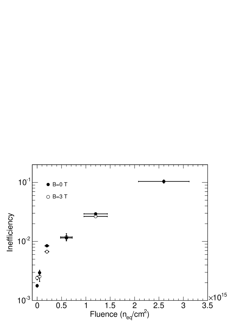
The particle detection inefficiency is well below 1% for unirradiated sensors but it increases with irradiation fluence. The inefficiency depends only weakly on the applied threshold. After a fluence of neq/cm2 the inefficiency is still below 2% and acceptable for the operation within CMS. For the sensors irradiated to fluences lower than neq/cm2 the undetected hits are uniformly distributed within the pixel cell [30]. At higher irradiation fluences the undetected hits are located mostly in the punch-through structure and along the metal line. This is due to the reduced charge collection in these regions, as discussed in Section 7.2.
By applying a 3 T magnetic field parallel to the horizontal axis of Fig. 10 charge carriers are deflected from the electric field lines and charge is spread over a region of about 50-130 m, depending on the amplitude of the Lorentz angle. The charge deflection is parallel to the vertical axis of Fig. 10. In this configuration, the detection inefficiencies related to the metal line are unaffected by the magnetic field, while the inefficiencies due to the punch-through structure are suppressed. Since the overall detection inefficiency after irradiation is dominated by the hits lost along the metal line the values measured with and without magnetic field generally agree.
7.4 Charge collection across the sensor bulk
As discussed in the previous sections, charge collection after heavy irradiation is affected by trapping of charge carriers. Electron and hole pairs produced by traversing particles drift to the sensor electrodes where the signal is induced. Particle irradiation produces defects in the silicon lattice which can trap these carriers and reduce the amplitude of the signal. Charges produced close to the sensor backplane and drifting for a longer distance are more likely to be trapped.
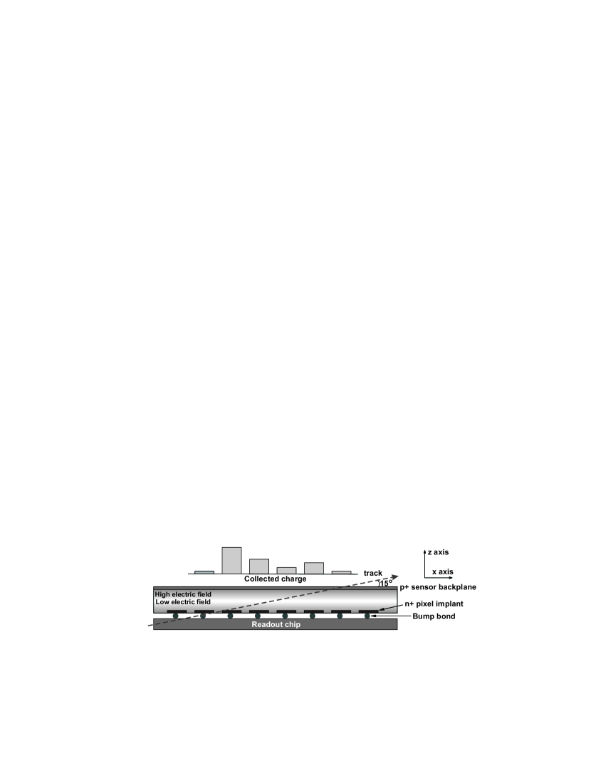
In pixel sensors, effects due to irradiation can be investigated with the so-called grazing angle technique [31]. As shown in Figure 12 the surface of the sensor is oriented at a small angle with respect to the hadron beam. The charge measured by each pixel along the direction samples a different depth in the sensor. The precise entry point from the beam telescope is used to produce finely binned charge collection profiles. The cluster length determines the depth over which charge is collected in the sensor.
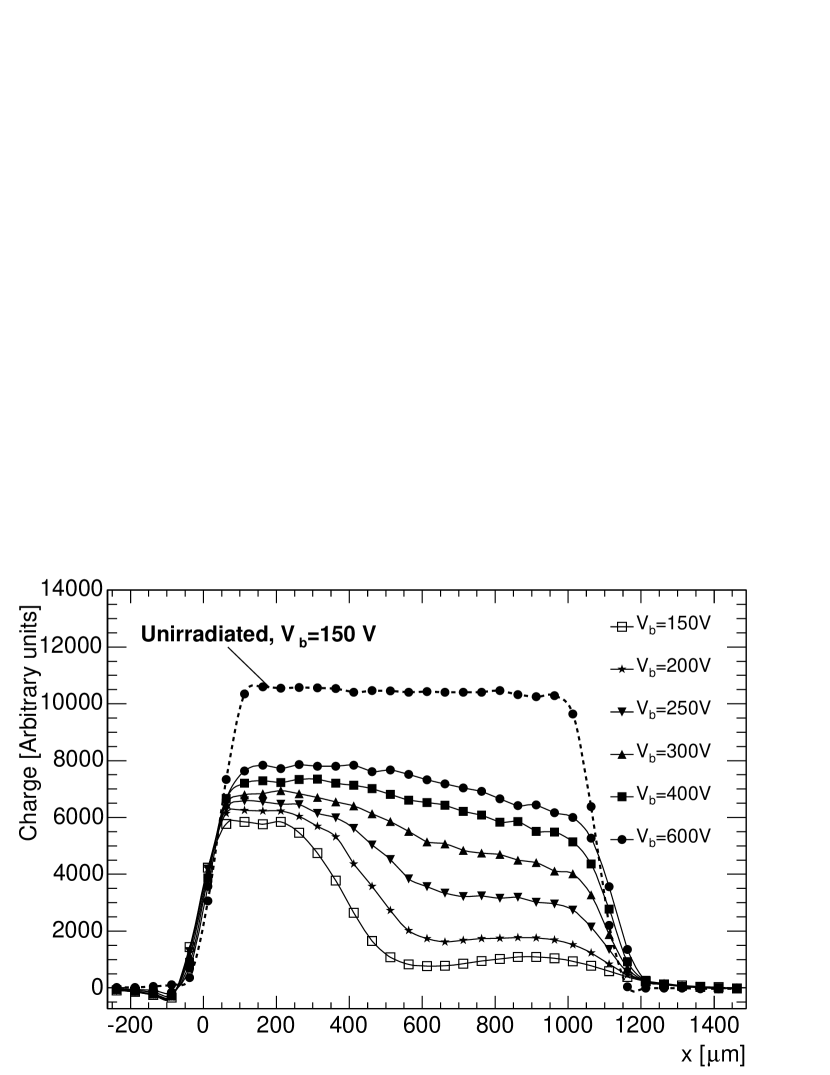
The profiles measured with an unirradiated sensor and with a sensor irradiated to a fluence of n are shown in Fig. 13 as function of the distance from the beam entry point. The unirradiated sensor was operated at a bias voltage of 150 V which is well above its depletion voltage (approximately 70 V). The profile of the collected charge is uniform and has sharp edges, indicating full depletion. The uniformity of the signal shows that no charge is lost when crossing the whole thickness of the sensor (a large coordinate corresponds a large collection distance), as expected for an unirradiated device. The irradiated sensor was operated at bias voltages between 150 V and 600 V. It appears to be partly depleted at 150 V, however, a second peak is observed at large . By increasing the bias voltage the amplitude of the second peak increases and more charge is collected from the sensor side close to the backplane, while the increase at the n+ side is about 30%. At 600 V charge collection is saturated but the profile is not as uniform as for the unirradiated case due to the trapping of carriers produced far from the collecting electrode.
The observed charge collection profiles do not correspond to the classical picture of a partially depleted sensor and even at low bias voltages charge is collected from the whole sensor thickness. In [8, 9, 10] it was demonstrated that the observed profiles can be described by a two trap model producing a non-constant space charge density across the bulk. This leads to electric field profiles with two maxima, one at each sensor edge. In particular, the high electric field at the sensor backplane is necessary to explain the tails at large observed in the charge collection profiles shown in Fig. 13. The model is supported by measurements of the electric field profile based on the field dependence upon electron mobility [32].
In the classical picture of a type inverted device with constant space charge density across the bulk the ratio is expected to grow as the square root of the bias voltage. The charge collection profiles were integrated along the coordinate and the integral measured with the irradiated sensors was divided by the value obtained with the unirradiated sensor operated at 150 V. Figure 14 shows this ratio as function of the square root of the bias voltage. The values are not corrected for possible gain and thickness differences among the samples.
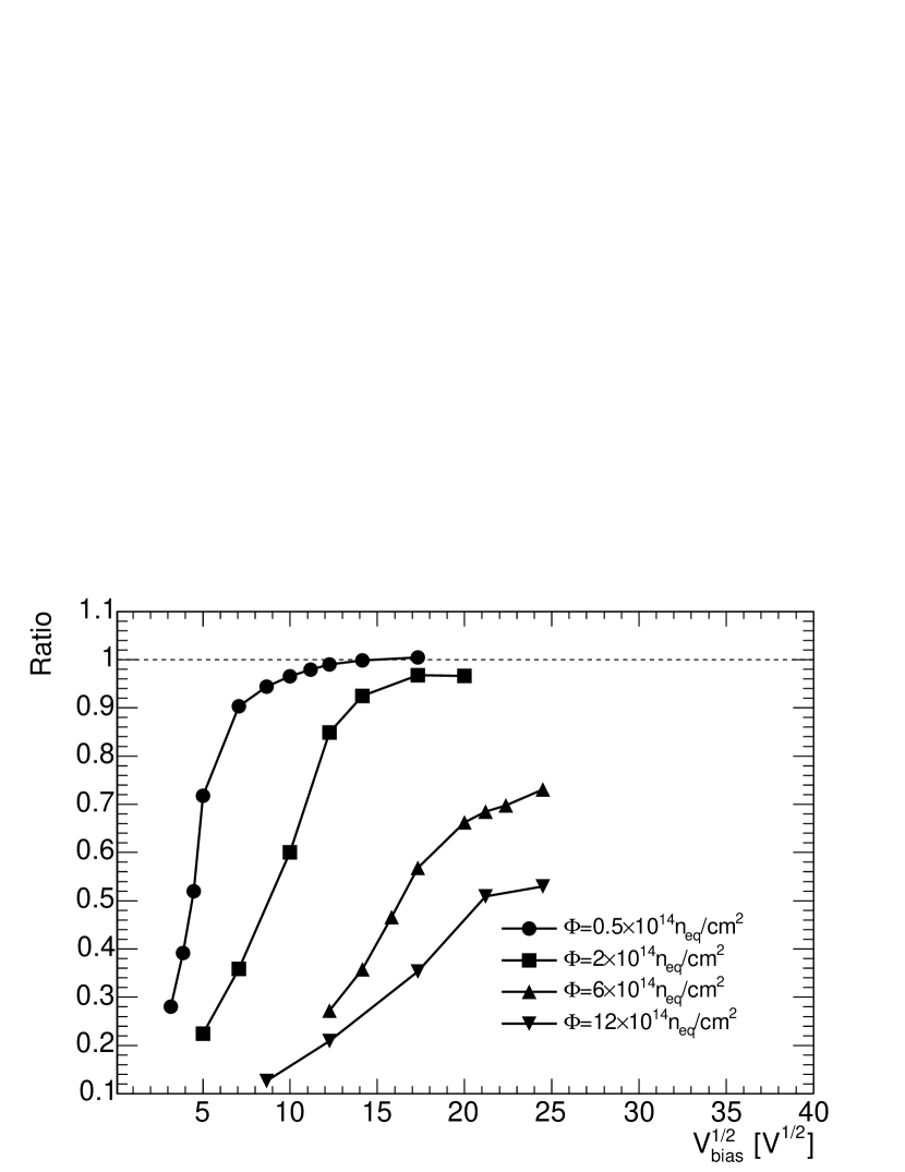
The charge ratio grows with increasing bias voltage and then reaches a plateau. With increasing irradiation the bias voltage at which the ratio saturates also increases, showing that the detector has to be operated at higher bias voltage to collect the same deposited charge. The measured ratio grows faster than the prediction as a consequence of the doubly peaked electric field profile.
7.5 Lorentz angle
In the presence of magnetic field the Lorentz force acts on the charge carrier, that are deflected from their drift along the electric field lines. The deflection angle (Lorentz angle ) can be measured with the grazing angle technique [33].
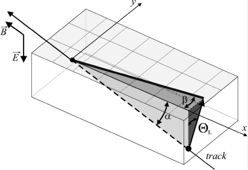
The beam crosses the sensor at a shallow angle and the charge carriers are deflected by the 3 T magnetic field parallel to the beam (see Fig. 15). By measuring the angle between the beam direction and the direction of the collected charge we derive the Lorentz angle
| (4) |
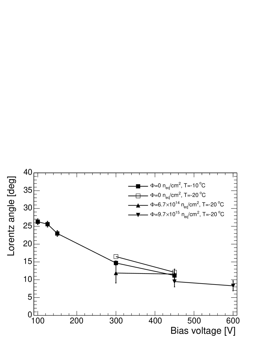
The average cluster profile is reconstructed using the track entry point predicted by the beam telescope. The cluster is sliced along the axis and the center of the each slice is measured along the axis. The angle is obtained by fitting the position of each slice as function of with a straight line [15]. A measurement without magnetic field is used to correct for detector misalignment with respect to the beam. Fig. 16 shows the Lorentz angle as function of bias voltage, extrapolated to 4 T magnetic field. The Lorentz angle decreases for increasing values of the bias voltage due to the dependence of the charge carrier mobility on the electric field. We expect the values measured at C to be about lower due to the increase of the electron mobility at lower temperature.
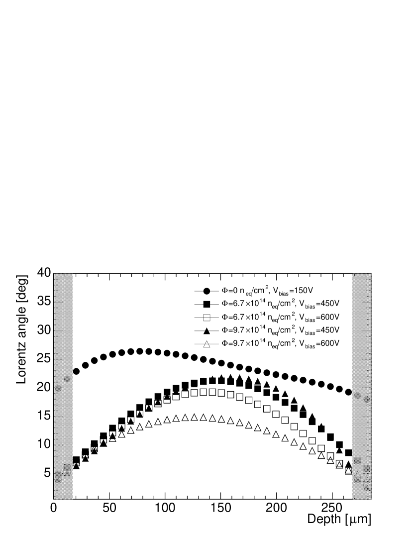
A straight line fit to the charge cloud implies a constant Lorentz deflection throughout the whole sensor thickness. A deeper analysis of our data sample shows that this assumption is valid only for unirradiated devices [32]. The Lorentz angle depends on the charge carrier mobility, which is a function of the electric field across the sensor and is given by
| (5) |
where is the Hall factor, is the projection of the magnetic field along the axis and is the carrier mobility. In an unirradiated sensor the electric field has a maximum at the backplane, where the reverse bias is applied, and decreases linearly with increasing depth. However, after irradiation, the doubly peaked electric field produces a Lorentz angle distribution with minima at the sensor edges and a maximum at medium depths. The Lorentz angle as function of depth in the sensor bulk is shown in Fig. 17 for irradiated and unirradiated sensors, where a zero depth corresponds to the n+ side of the device. The Lorentz angle is obtained from Eq. 5 and the measurement of the carrier mobility as a function of depth [32].
7.6 Spatial resolution
The reconstruction of the primary interaction and secondary vertices from heavy particle decays requires a good spatial resolution. The resolution of the pixel sensors is mainly determined by the readout pitch and charge sharing between neighbouring cells. Pixels have a weak capacitive coupling and charge sharing is mainly due to diffusion and drift of charge carriers under the combined effect of the magnetic and electric fields. After irradiation, free carriers trapping produces an inhomogeneous charge collection across the bulk and charge sharing between neighbouring pixels becomes strongly nonlinear on the impact position. In addition, the beneficial effect of the Lorentz deflection is reduced when a higher bias voltage is applied to provide a sufficient drift field. In what follows we discuss measurements of the sensor spatial resolution along the direction, where the charge drift is affected by Lorentz deflection.
For the measurement of the spatial resolution data were recorded with a 3 T magnetic field now perpendicular to the incoming beam. This corresponds to tracks in the experiment with rapidity . Events were first selected with the procedure described in Section 6.1. Pixels with charge above 2000 electrons were selected and clusters were formed by adjacent pixels above threshold. Both side and corner adjacent pixels were included in the cluster and a cluster threshold of 4500 electron was applied. When more than one cluster was found the cluster with the highest charge was used for the hit position measurement. To ensure that the cluster was entirely contained in the pixel sensor and well reconstructed, clusters adjacent to bad pixels or to the sensor border were rejected. For the irradiated detectors the background from noisy pixels was reduced by searching for further clusters in a fiducial region defined by a pixels window centered at the hit position predicted by the beam telescope.
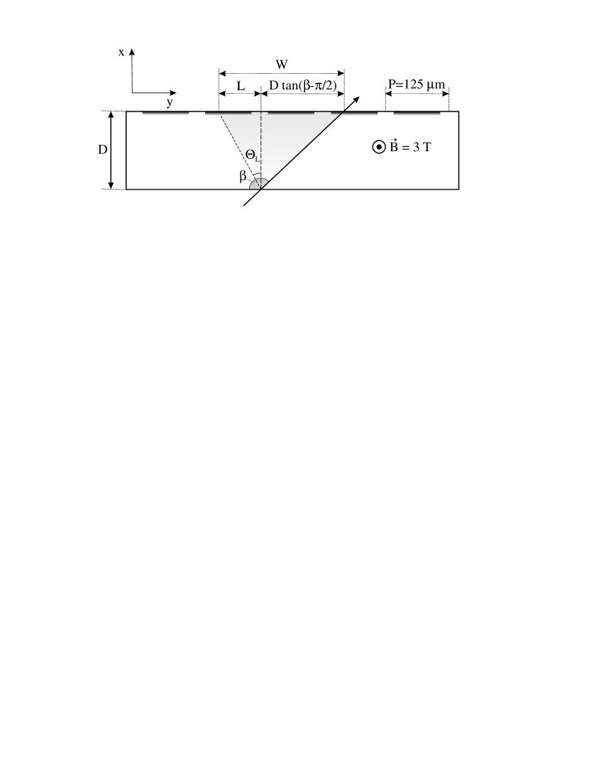
Figure 18 shows the definition of the track impact angle with respect to the sensor plane along the direction. The track is orthogonal to the sensor plane (parallel to the axis). The magnetic field in the direction produces a Lorentz shift toward the left direction (see Fig.18), thus, the total charge width is given by
| (6) |
The cluster is projected along the direction by summing the charge collected in the pixels with the same coordinate. For a cluster size of one the position is given by the center of the hit pixel. For larger clusters the hit position is determined by the expression
| (7) |
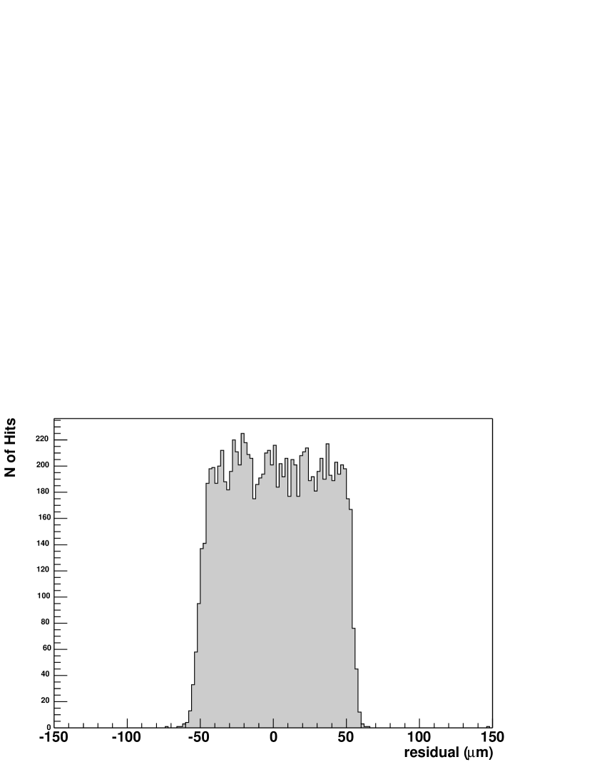
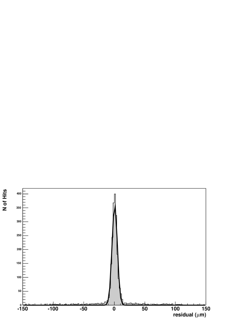
where () is the charge collected in the first (last) pixel above threshold and is the geometrical center of the cluster. The position resolution is obtained by comparing the reconstructed position with the prediction from the beam telescope, as explained in Section 6.2. We define as residual the difference between reconstructed and predicted position. For single pixel clusters the distribution is binary, as shown in Fig. 19. The residual distribution for clusters larger than one is shown in Fig. 19. It is approximately Gaussian with non-Gaussian tails which can be due to events where secondary electrons (or -electrons) are produced in addition to the electron-hole pairs. Scattered electrons can travel in the silicon lattice producing larger clusters, for which the reconstructed position is systematically displaced. Hereafter, the spatial resolution is given by the r.m.s. of the residual distribution for events with cluster size equal to one and by the of a Gaussian fit for larger clusters.
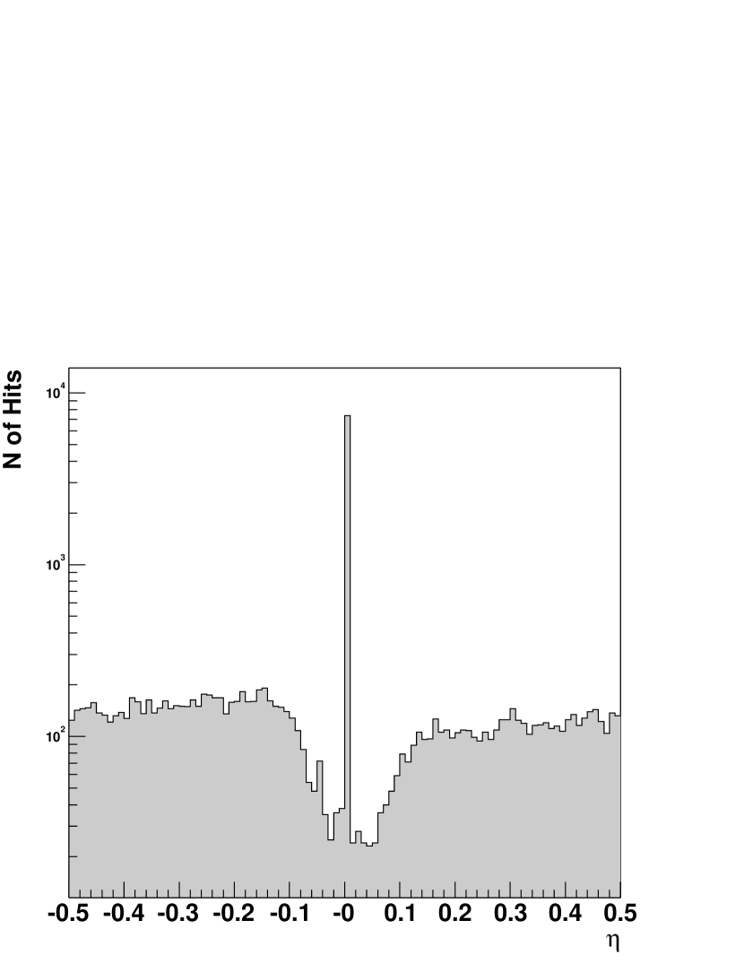
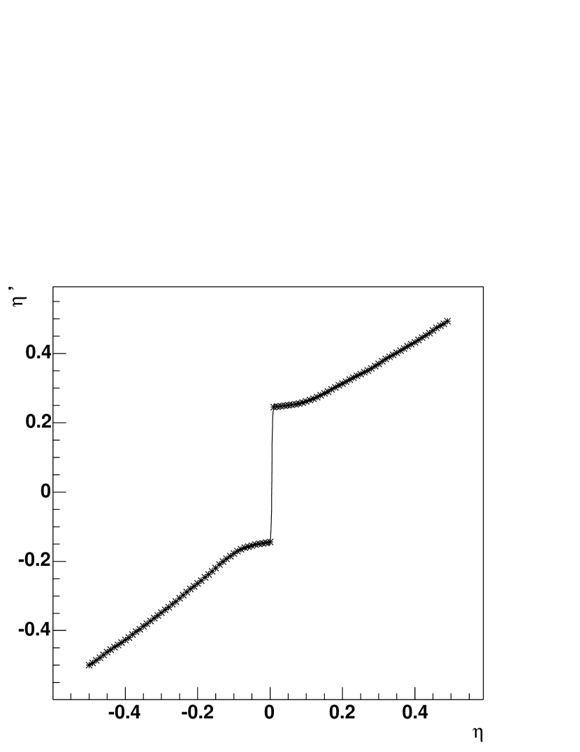
To further improve the spatial resolution for events in which charge is shared among several pixels the so-called -correction is used [28]. As we will show, the correction is particularly effective on irradiated devices, where the effects of inhomogeneous charge collection are larger. Assuming that the number of particles crossing the sensor is uniformely distributed along one expects that the reconstructed position within a pixel is also uniformely distributed. We define as the non-integer part of the position reconstructed from Eq. 7. Figure 20 shows the -distribution for all events, where corresponds to the center of the pixel cell and to its borders. The measured distribution is almost flat in the pixel regions closer to the pixel borders and it shows a dip at the center. The peak around zero is due to clusters of unit size. The -correction consists in rescaling the reconstructed position in order to obtain a flat hit distribution. For each we associate a corrected value given by the function
| (8) |
where is in pixel units. The function is shown in Fig. 20.
The position resolution is shown in Fig. 21(a-c) as function of the impact angle and for different irradiation fluences. The best resolution for clusters of size bigger than one is achieved at , for which the track direction is parallel to the Lorentz drift direction. In this case the charge width in Eq. 7 has a minimum and charge sharing can occur only when the particle crosses the region between neighbouring pixels. The width of this region is only approximately 20 m and the position can be reconstructed with about 4 m precision. However, these events constitute only about 10% of the event sample, which is dominated by single pixel clusters. The position of the resolution minimum is not constant and depends on the bias voltage applied to the sensor. The position resolution measured with the -correction is also shown in Fig. 21(a-c). With increasing irradiation, trapping of charge carriers produces nonlinear charge sharing between pixels which can be largely corrected with this method. In particular, larger corrections are observed for the wide charge distributions obtained when the track is not parallel to the Lorentz shift direction. After a fluence of n and for straight tracks the precision on the impact position can be improved by a factor two when the -correction is applied.
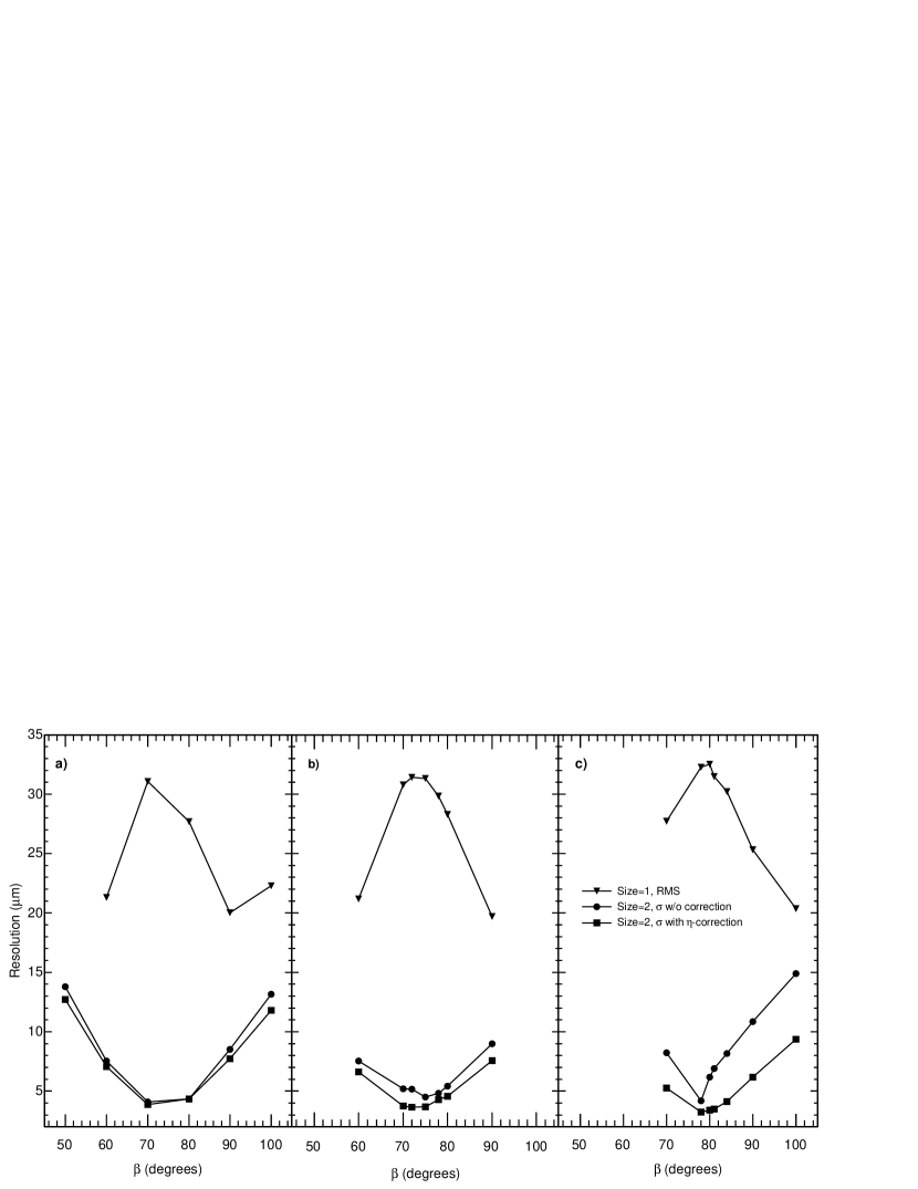
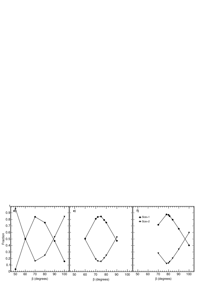
Figure 21(a-c) also shows the position resolution for single pixel clusters. In this case, the RMS of the residual distribution is equal to the width of the pixel cell region in which there is no charge sharing, divided by . Since the region has a maximum width for at this value the residual width is also maximal. As for clusters of larger size, the position of the maximum depends on the bias voltage. A larger bias voltage produces a smaller Lorentz angle, therefore the maximum is shifted towards larger . For higher or lower values of the residual width is smaller and the fraction of hits with charge sharing increases.
The fraction of clusters of size one and two is shown in Fig. 21(d-f) as function of impact angle. For the fraction of clusters with more than one pixel is around 50% before irradiation, decreasing to 35% at n.
In the final CMS pixel detector sensors with a readout pitch of m2 will be used. In addition, the CMS magnetic field will be of 4 T. With a smaller readout pitch along the direction the fraction of hits with charge sharing is expected to increase with a consequent improvement of the overall position resolution. In absence of beam test measurements, the expected position resolution can be estimated with a sensor simulation implementing a model of radiation damage [34, 35]. The model includes two defect levels with opposite charge states and trapping of charge carriers. The simulation shows that a position resolution below 15m along the CMS plane can be achieved after an irradiation of n.
8 Conclusions
The performance of the silicon sensors for the CMS barrel pixel detector were investigated in beam test measurements performed at the H2 beam line of the CERN SPS. The pixel cell size of the test sensors was 125125 m2. We expect the basic properties of the final sensor design (100150 m2 cell size) to be similar except for the spatial resolution.
The main results presented in this paper can be summarized as follows:
-
•
A signal over noise ratio S/N 65 was achieved with unirradiated sensors. At the specified fluence the S/N ratio is 50.
-
•
For unirradiated sensors charge is uniformly collected within the pixel implant with exception of the punch-through structure where the collected signal is 50% lower. However, the effect of the punch-through structure on the overall sensor performance is very limited as it represents only the 2-3% of the total surface. In the CMS experiment the effect will be further reduced by charge deflection due to the magnetic field.
-
•
The hit detection inefficiency is for unirradiated sensors and applying a threshold of 2000 electrons. After a fluence of the inefficiency is below 2% and is still acceptable for the operation within CMS.
-
•
The ratio of the charge collected by irradiated sensors divided by the charge collected by an unirradiated sensor operated at 150 V was measured as function of the bias voltage using the grazing angle technique. For a sensor irradiated at this ratio is larger than 60% for V V.
-
•
The Lorentz angle for an unirradiated sensor and a 4 T magnetic field is at 150 V and decreases at higher bias voltages. After irradiation we observe a Lorentz angle distribution across the sensor thickness with minima at the sensor edges and a maximum at medium depths which is consistent with a doubly peaked electric field.
-
•
The position resolution for perpendicular tracks and clusters of two pixels is m along the coordinate with Lorentz shift. This precision can be achieved also after irradiation by applying the -correction to reconstructed position. For clusters of a single pixel the residual distribution has RMSm for unirradiated sensors and m for .
Acknowledgments
We gratefully acknowledge the contribution from Silvan Streuli (ETH Zürich) and Fredy Glaus (PSI) for their immense effort with bump bonding, Federico Ravotti, Maurice Glaser and Michael Moll (CERN) for carrying out the irradiation, Kurt Bösiger (Zürich University) for the mechanical construction, György Bencze and Pascal Petiot (CERN) for the H2 beam line support and, finally, the whole CERN-SPS team.
References
- [1] The CMS Collaboration, CMS Tracker, Technical Design Report LHCC 98-6, CERN, Geneva, Switzerland (1998).
- [2] G. Lindstrom, et al., Radiation hard silicon detectors developments by the RD48 (ROSE) Collaboration, Nucl. Instrum. Meth. A466 (2001) 308–326.
- [3] Z. Li, H. Kraner, Fast neutron radiation effects in silicon detectors fabricated by thermal oxidation processes, IEEE Trans. Nucl. Sci 39 (1992) 577–583.
- [4] L. J. Beattie, et al., The electric field in irradiated silicon detectors, Nucl. Instrum. Meth. A418 (1998) 314–321.
- [5] G. Casse, E. Grigoriev, F. Lemeilleur, M. Glaser, Study of evolution of active volume in irradiated silicon detectors, Nucl. Instrum. Meth. A426 (1999) 140–146.
- [6] V. Eremin, E. Verbitskaya, Z. Li, The origin of double peak electric field distribution in heavily irradiated silicon detectors, Nucl. Instrum. Meth. A476 (2002) 556–564.
- [7] E. Verbitskaya, et al., The effect of charge collection recovery in silicon p-n junction detectors irradiated by different particles, Nucl. Instrum. Meth. A514 (2003) 47–61.
- [8] V. Chiochia, et al., Simulation of heavily irradiated silicon pixel sensors and comparison with test beam measurements, IEEE Trans. Nucl. Sci. 52 (2005) 1067–1075.
- [9] V. Chiochia, et al., A double junction model of irradiated silicon pixel sensors for LHC, Nucl. Instrum. Meth. A568 (2006) 51–55.
- [10] M. Swartz, et al., Observation, modeling, and temperature dependence of doubly peaked electric fields in irradiated silicon pixel sensors, Nucl. Instrum. Meth. A565 (2006) 212–220.
- [11] G. Bolla, et al., Design and test of pixel sensors for the cms experiment, Nucl. Instrum. Meth. A461 (2001) 182–184.
- [12] R. Kaufmann, Development of radiation hard pixel sensors for the CMS experiment, Ph.D. thesis, Universität Zurich (2001).
- [13] G. Bolla, et al., Sensor development for the cms pixel detector, Nucl. Instrum. Meth. A485 (2002) 89–99.
- [14] G. Bolla, et al., Irradiation studies of silicon pixel detectors for cms, Nucl. Instrum. Meth. A501 (2003) 160–163.
- [15] A. Dorokhov, et al., Tests of silicon sensors for the cms pixel detector, Nucl. Instrum. Meth. A530 (2004) 71–76.
- [16] T. Rohe, et al., Position dependence of charge collection in prototype sensors for the cms pixel detector, IEEE Trans. Nucl. Sci. 51 (2004) 1150–1157.
- [17] G. Bolla, et al., Design and test of pixel sensors for the cms experiment, Nucl. Instrum. Methods A 461 (2001) 182–184.
- [18] J. Kemmer, et al., Streifendetektor, Patent DE 19620081 A1.
- [19] T. Rohe, et al., Position dependence of charge collection in prototype sensors for the CMS pixel detector, IEEE Trans Nucl Sci 51 (3) (2004) 1150–1157.
- [20] R. H. Richter, L. Andricek, T. Gebhart, D. Hauff, J. Kemmer, G. Lutz, et al., Strip detector design for ATLAS and HERA-B using two-dimensional device simulation, Nucl. Instrum. Methods A 377 (1996) 412–421.
- [21] G. Lindström, M. Ahmed, S. Albergo, P. Allport, D. Anderson, L. Andricek, et al., Radiation hard silicon detectors – developments by the RD48 (ROSE) collaboration, Nucl. Instrum. Methods A 466 (2001) 308–326.
- [22] A. Bischoff, N. Findeis, D. Hauff, P. Holl, J. Kemmer, P. Klein, et al., Breakdown protection and long-term stabilisation for Si-detectors, Nucl. Instrum. Methods A 326 (1993) 27–37.
- [23] B. S. Avset, L. Evensen, The effect of metal field plates on multiguard structures with floating p+ guard rings, Nucl. Instrum. Methods A 377 (1996) 397–403.
- [24] M. Moll, E. Fretwurst, G. Lindström, Leakage current of hadron irradiated silicon detectors – material dependence, Nucl. Instrum. Methods A 426 (1999) 87–93.
- [25] C. Amsler, et al., A high resolution silicon beam telescope, Nucl. Instrum. Meth. A480 (2002) 501–507.
- [26] D. Meer, Bau und messen eines multichip pixelmodules als prototyp für den CMS-tracker, Master’s thesis, Eidgenössische Technische Hochschule, Zurich (2000).
- [27] A. Dorokhov, Performance of radiation hard pixel sensors for the CMS pixel detector, Ph.D. thesis, University of Zürich (2005).
- [28] E. Belau, et al., The charge collection in silicon strip detectors, Nucl. Instr. Meth. 214 (1983) 253.
- [29] T. Lari, Test beam results of ATLAS pixel sensors, hep-ex/0210045 (2002).
- [30] T. Rohe, et al., Fluence dependence of charge collection of irradiated pixel sensors, Nucl. Instrum. Meth. A552 (2005) 232–238.
- [31] B. Henrich, et al., Depth profile of signal charge collected in heavily irradiated silicon pixels, CMS Note 1997/021 (1997).
- [32] A. Dorokhov, et al., Electric field measurement in heavily irradiated pixel sensors, Nucl. Instrum. Meth. A560 (2006) 112–117.
- [33] B. Henrich, R. Kaufmann, Lorentz-angle in irradiated silicon, Nucl. Instrum. Meth. A477 (2002) 304–307.
- [34] E. Alagoz, V. Chiochia, M. Swartz, Simulation and hit reconstruction of irradiated pixel sensors for the CMS experiment, Nucl. Instrum. Meth. A566 (2006) 40–44.
- [35] V. Chiochia, E. Alagoz, M. Swartz, Sensor simulation and position calibration for the CMS pixel detector, Nucl. Instrum. Meth. A569 (2006) 132–135.