Current-induced break of inversion symmetry in Si: optical second-harmonic generation induced by a dc current
Abstract
The dc-current-induced optical second-harmonic generation is observed at the surface of centrosymmetric single crystal of Si. Surface dc-current with density up to A/cm2 results in break of inversion symmetry of Si and induces optical second-harmonic generation with intensity that corresponds to the appearance of dipole second-order susceptibility m/V.
Optical second-harmonic generation (SHG) in reflection from the surface of centrosymmetric materials is attractive topic of studies from the very beginning of nonlinear optics and dates back to the 1968’s experimental paper by N. Bloembergen and coworkers [1]. For this long-term period of studies and applications SHG was recognized as versatile powerful probe of surfaces and nanostructures [2]. High surface and interface sensitivity of SHG was a base of the broad family of nonlinear optical characterizations. Important role in these probes belongs to the studies of SHG under external impacts. The dc-electric-field-induced SHG (EFISH) [3] and dc-magnetic-field-induced SHG (MSHG) [4] are broadly used nowadays for characterization of electron and magnetic properties of surfaces and nanostructures.
Silicon is one of the materials thoroughly studied be means of the surface SHG. Apart from the general interest to this semiconductor, Si serves as basic model of the centrosymmetric material for nonlinear optical studies. Centrosymmetric materials are very specific in nonlinear optics as all even-order nonlinear susceptibilities vanish away in this class of materials [5]. As a consequence, SHG is strongly forbidden in the balk of centrosymmetric materials in dipole approximation due to symmetry selection rules. Anyway, the weak second-order susceptibility of the bulk still exists and is attributed to the quadrupole contribution. This quadrupole susceptibility is responsible for a weak background SHG contribution originating from the bulk. Basically this quadrupole SHG is the sole second-order nonlinear response in infinite samples of centrosymmetric materials.
Situation is significantly changed in semi-infinite samples: quite strong dipole surface SHG appears. There are three major mechanisms of the break of inversion symmetry at interfaces of centrosymmetric materials:
1. Inversion symmetry is broken at the boundary of semi-infinite sample due to the discontinuity of the crystallographic structure at the interface [6]. The thickness of surface layer with broken symmetry can be estimated as several periods of crystal lattice. The interfacial break of inversion symmetry results in appearance of dipole surface contribution that is dominant in reflected SHG.
2. Another mechanism of dipole reflected SHG is related to subsurface dc-electric field in space charge region (SCR) of semiconductors that appears in the vicinity of interfaces due to the band banding effect. A dc electric field in SCR, that is normal to the surface, breaks inversion symmetry in SCR and provides the strong EFISH contribution [7]. The thickness of SCR varies from several nanometers to a few hundreds of nanometers that depends on band banding potential and doping of semiconductor.
3. Third mechanism is related to the nonhomogeneous surface stress that also breaks inversion symmetry at interface and provides dipole susceptibility of surface layer and dipole reflected SHG [8]. The thickness of disturbed layer depends on stress relaxation and is in the range of several nanometers.
The corresponding nonlinear polarization of semi-infinite centrosymmetric crystal is given by the following formal equation:
| (1) |
where is quadrupole bulk susceptibility that originates from spatial dispersion and depends on wave vector k of fundamental field , is surface dipole susceptibility that originates from the break of the crystalline structure at the boundary of semi-infinite sample, is dipole susceptibility of SCR that appears from the break of inversion symmetry by dc electric field and is dipole surface susceptibility induced by strain which is described by strain tensor . For the last decades a number of experimental and theoretical works were devoted to the studies of these mechanisms of surface SHG in metals and semiconductors [9-11].
Generally, all these contributions to the SHG are attributed to the noncentrosymmetric distortion of the structure of the surface crystallographic unit cell. Initially centrosymmetric unit cell becomes noncentrosymmetric either due to existence of surface boundary or appearance of strong dc electric field due to band bending and inhomogeneous surface stress in surface layer, e.g. due to lattice missmatch between Si and SiO2.
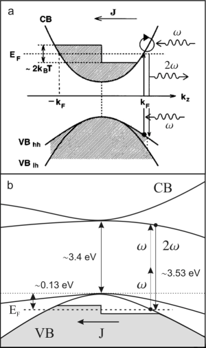
Meanwhile, apart from these contributions conditioned by noncentrosymmetric distortions of crystalline lattice one more mechanism of the break of inversion symmetry exists that is almost missed so far. The dc current flowing through semiconductor distorts equilibrium distribution function of electrons in quasi-impulse domain. This breaks inversion symmetry of electron subsystem of centrosymmetric semiconductor and results in appearance of the new term in Eq. 1: , where j is current density and is corresponding current-induced susceptibility. Theory of dc-current-induced SHG (CISH) in model direct band n-doped semiconductor is developed by Khurgin in Ref. [12]. Figure 1a shows schematic view of band structure of direct band semiconductor with electron distribution function in conduction band disturbed by a dc current (from Ref. [12]). Distribution of electrons is asymmetric for and , where is electron quasi-impulse. Perturbation theory approach results in appearance of current-induced term in second-order susceptibility with sharp resonance in the vicinity of local Fermi level for majority carriers in conduction band, . From theoretical consideration it follows that , where and that implies that current should break inversion symmetry of centrosymmetric materials. Symmetry analysis shows that for s-in, s-out combination of polarization of the fundamental and SH waves, respectively, the CISH signal appears as j is normal to the plane of incidence: for transversal geometry, and vanishes as j is in plane of incidence: for longitudinal geometry.
In this Letter current-induced break of the inversion symmetry and dc-current-induced SHG are observed in centrosymmetric Si. Three-fouled objective is targeted in these studies: relation between symmetry properties of electron subsystem and transport phenomenon in semiconductor, new nonlinear optical effect in nonequilibrium semiconductor, new probe for characterization and imaging of surface current distribution at semiconductor surfaces and interfaces.
There are the following points in realization of this experiment:
1. Fabrication of silicon structure that allows to pass dc current with density high enough to induce noncentrosymmetric perturbation of electron distribution function.
2. Selection of experimental conditions to avoid the influence of all other contributions except .
3. Selection of experimental conditions to avoid artefacts related to heating the samples by current.
4. The direct CISH effect should be distinguished from the in-plane EFISH effect, i.e. SHG induced by the dc electric field , that drives in-plane dc current.
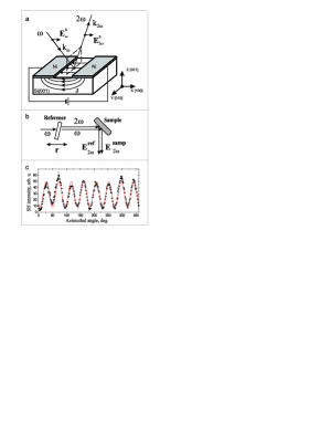
Figure 2a shows schematic view of Si structure for observation of the CISH effect. Highly p-doped (B-doped, cm) Si(001) wafer is used as substrate for experimental structure. Square-shaped (approximately of 0.5 cm0.5 cm area) Ni-electrodes are deposited on top of Si(001) wafer with native oxide by thermal evaporation of Ni in residual vacuum torr. The gap between Ni-electrodes is oriented along Y crystallographic axis. The width of the gap is 20020 microns. The thickness of Ni film is 30020 nm. After deposition of Ni stripes the samples were annealed to form Ohmic contacts between Si wafer and Ni electrode in accordance with procedure described elsewhere [13]. Contacts exhibit linear dependence and Ohmic resistance of approximately 0.02 . Maximum voltage applied to electrodes without noticeable heating is up to 0.5 V. The samples are mounted on special cooler stage to reduce the heating. Directly measured temperature of the sample during nonlinear optical experiments is less than 40∘C. Estimated current density in subsurface layer with the thickness of 50 nm, that corresponds to the escape depth of the SHG radiation at wavelength = 390 nm, is approximately .
The output of an unamplified Ti:sapphire laser with a tuning range of wavelength from 710 nm to 850 nm, a pulse duration of 80 fs, spectral bandwidth of 10 nm, an average power of 130 mW and repetition rate of 86 MHz is used as the fundamental radiation in nonlinear optical studies. The train of femtosecond pulses at a 45 angle of incidence is focused onto the Si(001) surface in the 200 micron gap between Ni-electrodes in sport with diameter of 40 microns.The SHG radiation is filtered out by appropriate glass bandpass and interference filters and is detected by a photo-multiplier tube and a gated photon-counting electronics. A fraction of the fundamental laser beam was split off to generate a SH reference signal from a crystalline Z-cut quartz plate, which normalized against drifts in average laser power and pulse duration during data acquisition. A detection system in ”reference” arm is identical to that in the ”sample” arm.
To distinguish between current-induced and heating-induced effects this is worth noting that current-induced susceptibility changes its sign under reversal of current direction. This implies that the nonlinear optical probe of the CISH effect should be sensitive to the current direction. The dc-current-induced SHG is studied by means of the SHG interferometry [14] with external homodyne reference [15]. Figure 2b shows the experimental scheme of the nonlinear optical interferometry. A 30 nm thick indium-tin-oxide (ITO) film on a glass substrate is used as homodyne reference.
The total SHG intensity from the sample and the reference depends on current density, current direction, the reference displacement, , and is given by:
| (2) |
where and are complex amplitudes of the current-reversal and current-independent SH fields from sample and reference, respectively; , , and are real amplitudes and phases of SH fields, respectively; is the coherence coefficient of the fundamental beam, is period of interference pattern and describes the dispersion of the refractive index of air, , at the SH and fundamental wavelengths, respectively. Interference of two components of the SH field results in appearance of homodyne cross-term that changes its sign under current reversal and oscillates as a harmonic function of the reference displacement. The dc-current-induced SHG is characterized by the CISH contrast, which is given by:
| (3) |
To avoid the influence of current sensitive variations of the SHG intensity related to EFISH and the stress-induced SHG the azimuthal anisotropic properties of SHG from Si(001) are used. From Refs. [6] it follows that for s-in,s-out combination of polarizations of the SH and fundamental waves the anisotropic SH response from Si(001) originates only from quadrupole bulk term whereas other terms from Eq. 1 vanish away: these terms contribute to SHG as p-polarized component exists either for SH or fundamental fields. Moreover, one can get rid of quadrupole bulk contribution for proper mutual azimuthal orientation of Si(001) wafer and incident plane of fundamental radiation. Figure 1c shows dependence of intensity of the bulk quadrupole SHG on the azimuthal angle for the s-in,s-out combination, , that demonstrates eight-fold symmetry. If plane of incidence is set at the angle that corresponds to zero of , this gets rid of the last contribution allowed for s-in, s-out combination. It means that in these experimental conditions the SHG intensity gets its zero value within the experimental error bar and one can expect observation of the CISH signal on this ”zero background”.
Thus, at ”zero background” conditions of interferometric experiment in transversal geometry of electrical bias we expect appearance of the CISH signal that should be sensitive to reversal of j and linear with respect to as this is proportional to interferometric cross-term in Eq. 2, and vanishes under transition to longitudinal geometry.
It turns out in experiment, the current reversible CISH signal appears in the external homodyne SHG interferometry for s-in,s-out combination and transversal geometry: Figure 3a shows dependence of on reference displacement. The solid line is result of approximation by oscillatory part of Eq. 3 with = 4.8 cm that is in good agreement with at wavelength of 780 nm [16]. The interferometric scheme allows to maximize value: further measurement are performed at corresponding to the maximum on dependence of on . The analogous measurements of are performed for s-in,s-out combination and longitudinal geometry. Figure 3a demonstrates the lack of the CISH effect for the longitudinal geometry: the detected SHG signal remains be equal to ”zero background” within the experimental error bar.
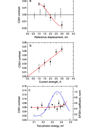
Figure 3b shows linear dependence of on at fixed position of reference with respect to the sample, which corresponds to the measurements of current dependence of in accordance to Eq. 3. The linear current dependence of reveals analogous dependence of interference cross-term in Eq. 3 and as a consequence linear dependence of on .
There is the only one source of the SHG signal, which can disguise the CISH effect in our experimental conditions. This is in-plane EFISH. Two experimental arguments prove that the SHG signal that accompanies a dc current corresponds to the direct CISH effect instead of the in-plane EFISH.
The first argument is comparison of the expected value of the in-plane EFISH signal from our in-plane biased Si and EFISH signal from space charge region of Si in biased metal-oxide-semiconductor (MOS) capacitors. The ratio of these EFISH signals is proportional to the squared ratio of the corresponding dc electric fields: [17]. The value of the in-plane dc electric field V/m is typical for our Si structure and experimental conditions. Whereas typical value of the dc electric field normal to the surface is V/m [18]. Expected ratio of EFISH signals is . Meanwhile, the absolute value of the CISH contribution to the SHG intensity can be recalculated from . The corresponding ratio that is by two orders of magnitude large than for the estimated in-plane EFISH contribution.
Another argument is comparison of spectral dependence of the CISH and EFISH effects in p-Si(001). Figure 3c shows spectral dependencies of the CISH contrast measured in our experiments and the EFISH coefficient from Ref. [18]. Comparison of these spectra shows the difference that prove our conclusion that observed current-induced variations of the SHG intensity are not related to the EFISH effect. Moreover, spectral dependence of the CISH signal is in qualitative agreement with results of model consideration in Ref. [12]. Figure 1b shows schematically the band structure of Si. In the case of -doped Si distribution function for holes is similar to that for electrons considered in Ref. [12]. Local Fermy level for holes at room temperature for our highly -doped Si wafers is 0.130.01 eV below the bottom of valance band at =0. This implies that sharp CISH resonance (Khurgin resonance) is expected approximately at 3.53 eV whereas the SHG spectroscopy in Figure 3c cover the spectral range below 3.4 eV that is restricted by the tuning range of Ti:sapphire laser. Slightly arising spectral dependence of the CISH contrast in Figure 3c can be qualitatively associated with the low-energy wing of the temperature broadened Khurgin resonance.
Comparison of the CISH signal with reflected SHG from crystalline quartz which dipole second-order susceptibility is known from handbooks [19] allows to estimate maximum magnitude of the CISH susceptibility m/V and the CISH coefficient m2/A, which is defined by: .
In conclusion, the dc-current-induced optical SHG is observed in centrosymmetric single crystal of Si. dc current with surface density up to A/cm2 induces optical SHG with intensity that corresponds to the second-order susceptibility m/V. Details of the CISH experiment: azimuthal orientation of Si(001) surface, polarization combination, the SHG interferometry and spectroscopy techniques, prove the mechanism of the SHG current dependence that is current-induced break of inversion symmetry of Si. Observation of the CISH effect opens perspectives of this novel surface probe in characterization of semiconductor devices: surface current imaging and mapping.
References
- (1) N. Bloembergen, R.K. Chang, S.S. Jha, Phys. Rev., 174, 813 (1968).
- (2) Y.R. Shen, Nature (London), 337, 519 (1989).
- (3) S.H. Lee, R.K. Chang, N. Bloembergen, Phys. Rev. Lett. 18, 167 (1967).
- (4) Ru-Pin Pan, H.D. Wei, Y.R. Shen, Phys. Rev. B, 39, 1229(1989).
- (5) Y.R. Shen, The Principles of Nonlinear Optics. (Wiley, New York, 1984).
- (6) H.W.K. Tom, T.F. Heinz, Y.R. Shen, Phys. Rev. Lett. 51, 1983 (1983).
- (7) J.I. Dadap, X.F. Hu, M.H. Anderson, M.C. Downer, J.K. Lowell, O.A. Aktsipetrov, Phys. Rev. B 53, 7607R (1996).
- (8) W. Daum, H.-J. Krause, U. Reichel, H. Ibach, Phys. Rev. Lett. 71, 1234 (1993).
- (9) T.F. Heinz, in Nonlinear Surface Electromagnetic Phenomena, H.-E. Ponath and G.I. Stegeman, eds. (North Holland, Amsterdam, 1991).
- (10) J.F. McGilp, Phys. Stat. Sol. A 175, 153(1999) .
- (11) G. Lüpke, Surf. Sci. Rep. 35, 75 (1999).
- (12) J.B. Khurgin, Appl. Phys. Lett. 67, 1113 (1995).
- (13) A. Singh, W.S. Khokle, Proceedings of the IEEE 75, 852 (1987).
- (14) G. Berkovic, Y.R. Shen, G. Marowsky, and R. Steinhoff, J. Opt. Soc. Am. B 6, 205 (1989).
- (15) J.I. Dadap, J. Shan, A.S. Weling, J.A. Misewich, A. Nahata, T.F. Heinz, Opt. Lett. 24, 1059 (1999).
- (16) O.A. Aktsipetrov, E.D. Mishina, T.V. Misuryaev, A.A. Nikulin, V.R. Novak, R. Stolle, and Th. Rasing, Surf. Sci. 402-404, 576 (1998).
- (17) O.A. Aktsipetrov, A.A. Fedyanin, V.N. Golovkina, T.V. Murzina, Opt. Lett. 19, 1450 (1994).
- (18) O.A. Aktsipetrov, et al. Phys. Rev. B, 60, 8924 (1999).
- (19) R.J. Pressley, edit. Handbook of lasers with selected data on optical technology. (Chemical Rubber Co. Cleveland, 1971).