Design of mid-IR and THz quantum cascade laser cavities with complete TM photonic bandgap
Abstract
We present the design of mid-infrared and THz quantum cascade laser cavities formed from planar photonic crystals with a complete in-plane photonic bandgap. The design is based on a honeycomb lattice, and achieves a full in-plane photonic gap for transverse-magnetic polarized light while preserving a connected pattern for efficient electrical injection. Candidate defects modes for lasing are identified. This lattice is then used as a model system to demonstrate a novel effect: under certain conditions - that are typically satisfied in the THz range - a complete photonic gap can be obtained by the sole patterning of the top metal contact. This possibility greatly reduces the required fabrication complexity and avoids potential damage of the semiconductor active region.
I Introduction
Quantum cascade (QC) lasers are semiconductor laser sources based on intersubband (ISB) transitions in multiple quantum well systems Gmachl et al. (2001). Their emission wavelength can be tuned across the mid-infrared Diehl et al. (2006); Darvish et al. (2006) (mid-IR, 5 m 24 m) and THz Williams et al. (2005) (65 m 200 m) ranges of the electromagnetic spectrum. In the mid-IR, where they are becoming the semiconductor source of choice thanks to their good performance, the potential applications are chemical sensing, spectroscopy and free-space optical communications. In the THz range the most promising application is the imaging of concealed objects. Biological materials, semiconductor chip packaging and clothing are all THz-transparent (while they are opaque at shorter wavelengths), making THz imaging useful for security and medical applications.
Most of the activity in the QC laser field has concentrated on edge-emitting lasers due to the intrinsic transverse-magnetic (TM) polarization of ISB transitions, and corresponding difficulty in implementing vertical-cavity surface emitting lasers (VCSELs). Surface emission has been obtained, rather, by integrating second-order gratings on edge emitting devices Hofstetter et al. (1999); Schrenk et al. (2000) or by replacing the standard Fabry-Perot cavity with a photonic crystal (PC) resonator Colombelli et al. (2004a); Srinivasan et al. (2004). The latter solution, the application of photonic crystal technology to QC lasers Joannopoulos et al. (1995); Vurgaftman and Meyer (2003), is particularly appealing because of the flexibility that it allows the designer. Two-dimensional (2D) photonic crystals can be used to create localized microcavity laser sources that can be built as two-dimensional arrays on a single chipPainter and Srinivasan (2003); Painter et al. (1999) or for large-area, high-power, single-mode surface emitting laser sourcesImada et al. (2002).
Of particular importance in determining the properties of any photonic crystal structure is the effective refractive index contrast attainable. The higher the index contrast, the stronger the optical dispersion of the photonic bands and the greater the ability to localize, diffract, and reflect light within the photonic lattice. A high index contrast is therefore crucial for device miniaturization. In planar waveguide devices, the presence of a full optical band gap in two-dimensions is beneficial (although not completely necessary) in forming ultra-low-volume laser cavities with minimal optical loss. As is discussed in Ref.Meade et al. (1993), for 2D photonic crystals, TM optical band gaps are favored in a lattice of isolated high- regions. Unfortunately, this configuration is incompatible with an electrical injection device due to its non-connected nature and an alternate approach is required.
In this paper we study the use of a connected honeycomb lattice for creating 2D photonic crystal QC laser structures. We begin in Section II with a review of the properties of this 2D lattice via a planewave expansion (PWE) analysis. We show that a full 2D optical bandgap for TM polarization can be obtained in this connected lattice, and study the localized resonant modes that form around a simple point defect in the lattice. In Sections III and IV full three-dimensional (3D) finite-difference time-domain (FDTD) simulations are used to analyze the properties of the honeycomb lattice in two different vertical waveguide structures. Section III deals with mid-IR PC QC lasers. The real active-region and waveguide structure of a mid-IR surface-plasmon (SP) QC laser is considered. The high-index contrast in this waveguide structure is obtained by air holes that penetrate deeply into the semiconductor layers. Section IV focuses on THz PC QC laser waveguide structures. In the metal-metal waveguides of THz lasers we find that the effective index contrast, and therefore the photonic bandstructure, is strongly dependent on the waveguide thickness111A similar phenomenon occurs in guided membrane PC structures, where it is known that the extent of the photonic gap depends on the membrane thickness Johnson et al. (1999). However, in the dielectric membrane structures, beyond a critical membrane thickness further reduction in thickness does not increase the bandgap due to a loss of mode localization in the dielectric membrane. The double-metal waveguide structure does not suffer from such a loss of confinement.. In particular, below a certain critical waveguide thickness, a full photonic gap can be induced by the sole patterning of the metal layers. This novel effect could be useful for the development of a variety of THz lasers, including PC surface-emitting lasersSchubert and Rana (2006), due to the simple fabrication requirements.
II Two-dimensional analysis: planewave expansion
II.1 The planewave expansion method
The calculations of this section are based on a planewave expansion (PWE) method. It is a frequency-domain method that allows extraction of the Bloch fields and frequencies by direct diagonalization. The calculations were performed using the MIT Photonic Bands (MPB) simulation toolJohnson and Joannopoulos (2001). With the PWE method it is possible to compute the bandstructures and electromagnetic modes of perfectly periodic dielectric structures. Calculation of defect modes will be tackled in section II.3 using a super-cell approach.
II.2 Photonic crystal structure and TM gap
The 2D photonic crystal considered in this work is that of a honeycomb lattice, consisting of a hexagonal Bravais lattice with a basis of two air holes per unit cell (see Fig. 1(a)). The hole radius is and the lattice constant is . The reciprocal lattice is also hexagonal, with , and the high symmetry points of the lattice (see Fig. 1(b)). In the 2D simulations of this section the relative dielectric constant of the dielectric background is taken as (), corresponding to the index of refraction of most III-V semiconductor materials at frequencies below the energy gap.
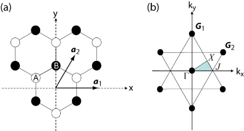
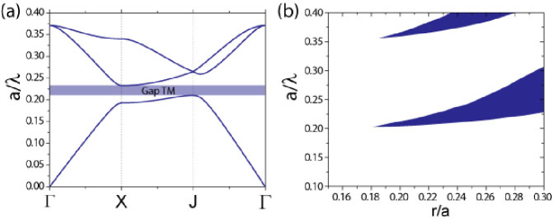
Fig. 2(a) shows the photonic bandstructure for a lattice with . For this ratio a full TM gap is present, centered around , with a width approximately of the central gap frequency. The existence of a gap, however, depends strongly on . In Fig.2(b) we plot the gap-map for this lattice, which clearly shows that only above a critical value of circular hole size () can a TM photonic gap be obtained. This is a common behavior of lattices of air holes; the larger the holes, the closer the lattice is to a system of isolated high- regions, and the larger the TM photonic bandgapJoannopoulos et al. (1995). The advantage of the honeycomb lattice is that the TM gap opens when the hole size and porosity of the lattice are still reasonably small, allowing for more efficient electrical injection.
II.3 2D defect design: supercell method
In this section we study, in 2D, the localized resonances that form around a point-like defect of the honeycomb lattice. The defect that we consider is obtained by removing a hexagon of six holes, as shown in Fig. 3(a). The defect modes are calculated with a supercell method using the same PWE solver. The presence of the defect cavity breaks the periodicity of the lattice, requiring the creation of a supercell over which the structure is assumed periodic. This supercell contains the defect cavity and is tiled in space. The Wigner-Seitz cell of the reciprocal lattice of the supercell will be correspondingly smaller than that of the underlying photonic lattice, resulting in a folding of the honeycomb lattice photonic bands (see Fig. 3(b)). The localized defect states of the supercell appear as bands with almost no dispersion, lying inside the photonic bandgap of the honeycomb lattice.
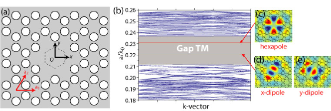
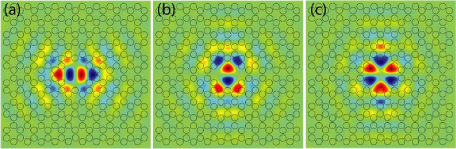
A PWE calculated bandstructure of the supercell defect structure with is shown in Fig. 3(b). In these calculations, a supercell consisting of 20 periods of the honeycomb lattice was used in order to obtain well localized resonant modes. Three defect modes lie within the complete band gap: two degenerate dipole-like modes and a hexapole-like mode (Figs. 3(c-e)). These are the defect modes that are predicted for the honeycomb lattice through simple symmetry arguments Painter and Srinivasan (2003). Of the defect modes present in the bandgap, the dipole-like modes are more concentrated in the center of the defect region, thus giving them the most overlap with the QC gain material. As such, these are the cavity modes we will focus on in the 3D simulations described below.
Our choice of hole radius () in the above cavity design was made based upon a trade-off between the extent of the photonic bandgap and cavity mode localization, with that of the electrical and thermal resistance incurred in a semiconductor realization of such a structure. As already mentioned, the reduced connectivity of a photonic lattice makes electrical injection of a defect cavity more challenging. Electrical current in such structures is typically injected from the edge of the photonic crystal vertically through the device active region. Injection into the defect region of the cavity is a result of lateral current spreading into the center of the photonic crystal. The increased lateral resistance of highly porous photonic lattices significantly reduces the injection efficiency of the laser, resulting in added heating and reduced gain. Other injection geometries are possible, such as the use of surface-plasmon laser cavities in which the top metal contact extends over the entire photonic crystal and provides not only vertical waveguiding but also electrical injection. This geometry was used in the demonstration of the first electrically injected 2D photonic crystal microcavity laserColombelli et al. (2004a). Nonetheless, high-aspect ratio 2D photonic crystal lattices of high porosity pose a greater challenge to fabricate due to the reduced critical dimension size. It should be noted that further optimization of the honeycomb lattice can be obtained through use of air holes of a modified geometry. Lattices formed from air holes with a truncated circular cross-section were found to have larger photonic bandgaps for a given critical dimension than that of the standard lattice. In what follows, however, we focus on the honeycomb lattice with circular air holes.
III 3D-FDTD analysis of mid-IR devices
The PWE method allows the rapid solution of structure eigenmodes in the frequency domain. However, for the 2D analysis described above one can only approximate the laser active region with an effective index of refraction. The objective of this section is to verify the design developed with the 2D model in Section II, and to apply it to a realistic mid-IR QC laser structure. An accurate representation of the structure waveguide in the epitaxial direction will be taken into account within a 3D finite-difference time-domain (FDTD) approach. It is well known that the material system of choice for mid-IR QC lasers is InGaAs/AlInAs lattice matched to InP Diehl et al. (2006); Darvish et al. (2006). In addition, waveguides based on surface-plasmons Bahriz et al. (2006) have been shown to be advantageous for PC QC lasers in the mid-IR Colombelli et al. (2004b). This is therefore the model system that we will use for the 3D simulations.
III.1 Mid-IR surface-plasmon waveguides for QC lasers
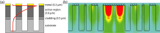
Semiconductor diode lasers and conventional QC lasers rely on optical waveguides where a higher-index-core is sandwiched between thick cladding layers of lower refractive index, thus confining the light inside the active region stack. The small refractive index difference between the active core and the waveguide claddings results in a standard mid-IR QC laser which is typically to m thick.
Maxwell’s equations, however, also allow for another type of optical waveguiding based upon surface-plasmonsRaether (1988). TM polarized electromagnetic guided modes exist at the interface of two dielectrics with opposite sign of the real part of their dielectric constants. Negative dielectric constants are typical of metals below the plasma frequency. Thus, guided surface-plasmon modes at a metal-semiconductor interface are a useful waveguiding solution for QC lasers Sirtori et al. (1998). This is due to the intrinsic TM polarization, i.e. normal to the layers, of intersubband transitions. SP waveguides need a smaller thickness of grown material, while yielding even larger optical confinement factors (see Fig. 4).
The surface-plasmon damping along the propagation direction can be approximated with the following formula Yeh (2005):
| (1) |
where () is the imaginary (real) part of the metal index of refraction, is the real part of the semiconductor index of refraction, and is the wavelength. The dependence of the propagation losses shows that SP waveguides are especially appealing at long wavelengths. In particular the factor, which pushes the field out of the metal region and reduces the losses, becomes very small at long wavelengths. A simple Drude model shows that the imaginary part of the index of refraction, for a generic metal, increases dramatically when moving from short (- m) to long (- m) wavelengths. Recent advances have also shown that low-loss metallic waveguides can be implemented at mid-IR wavelengths Bahriz et al. (2006). We therefore employ this waveguide structure as a model system for the 3D numerical simulations of our QC laser structures. The corresponding layer sequence is displayed in Table 1, together with the corresponding indeces of refraction that are used for the simulations.
| Material | Doping (cm-3) | Thickness (m) | Function | |
|---|---|---|---|---|
| air | n.a. | 4 | 1 | top cladding |
| Au | n.a. | 0.3 | perfect conductor | metal contact |
| InGaAs | 1017/1018 | 0.05 | 3.3/3.47 | contact layers |
| InGaAs-AlInAs MQW structure | 1.7 x 10¹⁶ | 2.6 | 3.374 | active region |
| InGaAs | 5 x 10¹⁶ | 0.5 | 3.475 | Buffer/lower cladding layer |
| InP | 1017 | 3 | 3.077 | substrate |
While the vertical confinement is provided by the SP waveguide, the in-plane optical confinement is induced by the photonic crystal. A high index contrast can be obtained by penetration of the air holes through the top metal layer and deep into the semiconductor waveguide structure. Intuitively, reduced scattering losses are obtained for a hole depth which overlaps a significant fraction of the guided mode energyD’Urso et al. (1998). In Fig. 5(a) we show a schematic of the vertical cross-section of the photonic crystal SP waveguide structure, and in Fig. 5(b) we plot the vertical mode profile of a localized defect mode (see Fig. 6(a)) of the honeycomb lattice of air holes with a hole depth of m in the semiconductor heterostructure. At an operating wavelength of m this results in a vertical mode overlap (energy overlap) with the air holes of almost . It is clear from this example why surface-plasmon QC lasers are ideally suited to PC technology; their reduced thickness allows for a significantly shallower etch of the semiconductor material in comparison to conventional laser waveguide structures in which an etch depth of m or more would be required in the mid-IR.
III.2 Defect cavity design
The cavity investigated in this section is the same as in Section II.3. It is obtained by removing a full hexagon of air holes from the PC lattice. As depicted in Fig. 5, we “etch” 4.7-m deep holes into the semiconductor laser structure, with the ratio of the air holes set to . The properties of the different laser structure layers used in the simulation are given in Table 1. Full 3D-FDTD simulationsPainter and Srinivasan (2003); Painter et al. (1999); D’Urso et al. (1998) were performed with an effective grid resolution of 100 nm, corresponding to roughly 20 points per wavelength in the high-index semiconductor material at an operating wavelength of m. The use of perfectly conducting boundaries for the top metal contact layer is a small approximation at m due to the much higher plasma frequency of the Au metal contacts used in practice.
A simulation of a photonic crystal cavity with periods in the -direction and periods in the -direction yields the three localized defect modes shown in Fig. 6(a-c). These modes are the same modes as found in the 2D analysis of Fig. 3. Comparison of the 2D and 3D mode properties are summarized in Table 2. The normalized frequencies of the defect modes lie within the TM-like bandgap of the 3D honeycomb lattice waveguide structure, and are centered around . At a wavelength of m this corresponds to a lattice constant of approximately m, a hole radius of m, and a minimum dimension given by the gap between nearest neighbor holes of m.
Effective quality factors associated with in-plane (), topside vertical (), and bottomside vertical () radiation losses are also calculated for the 3D FDTD simulations. The topside vertical effective -factor for all of the defect modes is estimated at , due to the fact that the cavity modes lie predominantly below the light cone of the top air-claddingSrinivasan and Painter (2002). on the other hand, can be increased only slightly from that reported in Table 2 through deeper etching of the air holes, limited mainly by the high-index of the semiconductor substrate and the localized nature of the cavity. Due to the TM-like polarization in-plane bandgap provided by the honeycomb lattice, an increase in the number of PC mirror periods to a value above effectively eliminates in-plane radiation loss, and the -factor of the cavity modes is limited by both radiation into the substrate as well as material absorption loss due to ohmic heating in the metal surface-plasmon layer (for wavelengths in the mid-IR, and a Au metal surface-plasmon layer, material absorption limits the -factor to approximately Srinivasan et al. (2004)).
| Parameter | -dipole mode | -dipole mode | hexapole mode |
|---|---|---|---|
| PWE | 0.2115 | 0.2115 | 0.2162 |
| FDTD | 0.196 | 0.197 | 0.205 |
| 326 | 288 | 169 | |
| 92 | 93 | 114 |
IV Analysis of THz devices
Our FDTD analysis of mid-IR PC QC lasers examined structures in which the honeycomb lattice was patterned through the QC semiconductor active region. This is necessary in order to induce a strong index contrast. However, a different solution is possible if the optical mode is highly confined in the vertical direction, as is the case for THz QC lasers with metal-metal waveguide structuresUnterrainer et al. (2002); Williams et al. (2003). In this case, and under certain constraints related to the structure thickness, the sole patterning of the top metal contact is capable of inducing a complete photonic bandgap. These metal-insulator-metal (MIM) structuresPrade et al. (1991), as we will refer to them here (see Figs. 7 and 8), will be the focus of our time domain modeling in the following sections. The appeal of this design lies in the fact that only the top metal layer needs to be patternedMahler et al. (2005); Demichel et al. (2006), which both simplifies the fabrication process and improves the efficiency of carrier diffusion in the active region.
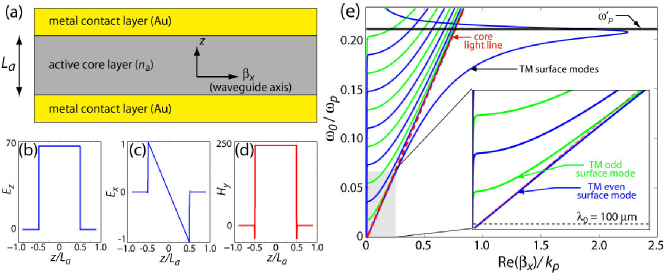
IV.1 MIM structures: waveguides for THz QC lasers
Metal-metal waveguidesPrade et al. (1991) are usually employed for QC lasers in the THz rangeUnterrainer et al. (2002); Williams et al. (2003) because they can provide almost unity optical confinement factors, and simultaneously, relatively low waveguide losses. The active laser core is sandwiched between two metal layers (typically Ti/Au or Ge/Au/Ni/Au) which act as surface-plasmon layers (Fig. 7(a)). The two surface-plasmon modes of both the top and bottom metal-core interfaces become coupled and form two guided modes, one of even parity and one of odd parity (assuming a nearly symmetric metal-core-metal structure, and where the vector parity is determined by the symmetry of the magnetic field). The dispersion diagram of a double-metal waveguide with active layer core thickness of m is displayed in Fig. 7(e). For sub-wavelength core thicknesses the odd parity surface mode is cut-off, while the even parity mode exists all the way down to zero frequency. The electric and magnetic field profiles of the even parity surface mode at a wavelength of m are shown in Fig. 7(b-d), showing the near-unity confinement factor of the fields in the core region.
As has been noted by other authorsMaier (2006), a reduction in the dielectric core region thickness of MIM structures results in an increase in the in-plane wavevector of the even parity guided mode for a particular frequency. This is a result of the “pushing” of the electromagnetic energy into the metal cladding regions with decreased core thickness. Of import to the current work is the ability to create a large effective index contrast through patterning only of the metal layers. In such a patterned structure the guided mode sees two effective indeces as it propagates, the large effective index of the guided surface-plasmon mode where the metal is left intact, and a lower effective index, more delocalized mode of the dielectric core and air-cladding where the metal is removed. That this picture is in fact valid, and can be used to great effect, is demonstrated below where we analyze the bandstructure and localized resonances of double-metal waveguides with only a surface-patterning in the top metal contact.
IV.2 Patterned MIM waveguide bandstructure analysis
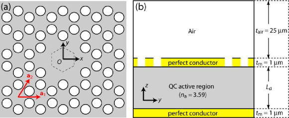
The model MIM structure that we will consider here, shown schematically in Fig. 8(b), consists of the following sequence of layers (from bottom to top): a bottom unpatterned metal contact, a QC active region dielectric core (modeled with a uniform index of for simplicityKohen et al. (2005)), a top patterned metal contact, and a region of air above the structure. The metal layers are assumed to be perfect conductors; loss due to absorption in the metal regions is discussed in section IV.4. Mur absorbing boundary conditionsMur (1981) are used to model radiation loss out of the structure. For each of the THz FDTD simulations described below, a grid resolution of points per lattice constant of the honeycomb lattice was used. At a nominal operating wavelength of m, and for normalized frequencies within the bandgap of the honeycomb lattice (see below), the lattice constant is m. At this wavelength and normalized frequency (hereinafter the nominal operating conditions), the corresponding spatial resolution is m (roughly points per wavelength in the dielectric core material), and the MIM layer thicknesses are as shown in Fig. 8(b).
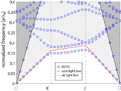
The band diagram for surface-patterned MIM waveguide structures with various dielectric core thicknesses were computed to confirm the existence of a complete in-plane bandgap, and to examine the dependence of the bandgap frequency width on structure thickness. The simulation volume consists of a single unit cell of the honeycomb lattice with Bloch periodic boundary conditions applied in the plane of periodicity and Mur boundary conditions in the top and bottom directions (normal to the metal and semiconductor layers). Figure 9 shows the band diagram for a structure with a normalized core thickness of and a normalized air hole radius of in the top metal layer. The corresponding physical core thickness is m under nominal operating conditions ( m, ). In the band diagram, truly guided modes lie below the air light-line, while leaky modes lie above it (in this case light can only leak into the top vertical direction where patterning of the metal has been applied). The bottom-most band is a surface wave, lying just below the light-line of the active region core. It is akin to the even parity guided surface-plasmon mode of the symmetric (unpatterned) double-metal waveguide studied above. The higher-lying frequency bands constitute zone-folded versions of this surface wave. An in-plane photonic bandgap exists for guided modes of this structure between normalized frequencies . Due to the extreme thinness of the dielectric core, the higher-order vertical modes of the MIM waveguide are not present in this diagram, but lie at much higher frequencies (). As a result, the photonic bandgap is a true full in-plane bandgap for guided resonances of the MIM structure, not just for a single polarization or mode symmetry. Note, the modes that lie along the air light-line in the diagram are radiation modes, predominantly localized in the air regions above the MIM structure.
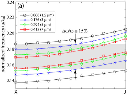
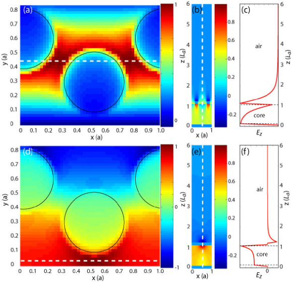
In Fig. 10 we plot the dispersion of the bands defining the (lowest) photonic bandgap between the high symmetry and points of the honeycomb lattice for varying dielectric core thicknesses. The bandgap is seen to shrink with increasing dielectric core thickness, closing for a normalized active region thickness greater than (nominal physical thickness m). Mode field plots (see Fig. 11) at the and points indicate that the high and low frequency modes defining the bandgap are of mixed type: the low-frequency “dielectric” or “valence” band mode is predominantly a surface wave at the interface of the top patterned metal surface, whereas the high-frequency “air” or ”conduction” band mode is predominantly a surface wave of the bottom unpatterned metal interface. Additionally, the high-frequency gap mode sits largely beneath the unpatterned regions of the top metal boundary and the low-frequency mode resides below the patterned areas with more energy residing in the air cladding. The photonic bandgap in this case is a result of differences in these two surface waves. This simple picture, although correct, betrays its complexity for two reasons: (i) perfect metal conductor boundaries were used in the simulations, which do not support surface waves when continuous and flat, and (ii) the patterned air holes are much smaller than the wavelength in air of the guided mode. That a surface wave can indeed exist at the interface of a patterned perfect conducting layer was pointed out in Ref. Pendry et al. (2004), where it was shown that it is precisely the cut-off frequency of the air holes in the perfect conductor which sets the effective plasma frequency of the layer. The thinner the dielectric core layer, the larger the fraction of energy that resides at the top patterned metal interface, and a greater degree of mode delocalization that occurs into the air-cladding where the top contact is removed, both effects which increase the effective index contrast of the two surface waves and thus the photonic bandgap. It should be noted that the use in our model of perfect conducting boundaries as opposed to a Au metal contact layer, for instance, does not affect the photonic bandstructure shown in Fig. 9 and Fig. 10, as the plasma frequency of Au is much greater than the THz frequencies under consideration. Further discussion and analysis of photonic bandgap structures formed from surface patterned metal and perfectly conducting layers will be presented in a future studyPainter and Colombelli . In practice, laser structures with thicknesses much below that of several microns may be difficult to fabricate and incur insurmountable optical losses (see below for discussion), but the trend shown in Fig. 10 clearly indicates that such structures would support complete bandgaps that are quite substantial, approaching of the gap center frequency for m at an operating wavelength of m.
IV.3 Characterization of defect modes
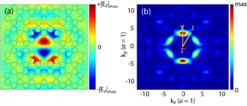
Ultimately, one would like to utilize the strong photonic bandgap effects present in the patterned MIM waveguide structures studied above to, for instance, form localized microcavity laser resonators. In order to demonstrate the effectiveness of the top metal patterning in this regard, we have also simulated the localized resonances that are formed within and around point defects of the honeycomb metal pattern studied in the previous sub-section. In Fig. 12(a) we show the field plot of the localized -dipole-like222The symmetry of the mode is that of a -polarized dipole in the plane of the MIM waveguide. It is degenerate with a second dipole-like mode with -polarizationPainter and Srinivasan (2003). mode that forms around a point-defect consisting of the removal of the central 6 holes in the top metal (see Fig. 8(a)) of a MIM waveguide with an active region thickness of m (). The corresponding (in-plane) spatial Fourier transform of the mode is plotted in Fig. 12(b), showing that the mode is localized at the points in reciprocal space, and consistent with a “donor” mode formed from the “conduction” bandedge at the -pointPainter and Srinivasan (2003). This mode is identified as the same dipole-like mode of the mid-IR surface-plasmon simulations of Fig. 6(b) in section III, where in those structures a deep air hole patterning of the semiconductor dielectric material was used to create a large index-contrast.
For the fixed waveguide core thickness of m the -dipole-like mode of Fig. 12(a) is seen to be highly localized in real-space, as expected from the bandgap simulations of Fig. 10. Additional confirmation of the in-plane localization of the defect mode due to an in-plane photonic bandgap effect can be obtained by studying the scaling of the in-plane radiation losses as a function of the number of periods of the PC patterning surrounding the central defect. The total quality factor due to radiation loss is determined by
| (2) |
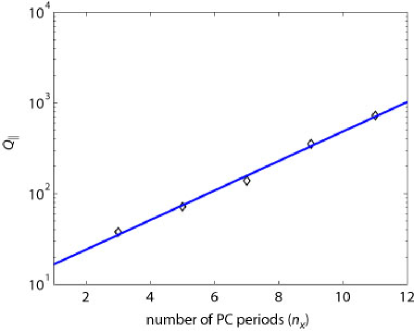
where and quantify the in-plane and out-of-plane radiation lossesPainter et al. (1999). The out-of-plane quality factor is found to be for these structures; thus the dominant radiation loss occurs in the in-plane direction. Fig. 13 shows a plot of the -factor as a function of the number of surrounding PC periods. The radiation -factor increases exponentially with period number as expected for a bandgap mode, with a cavity consisting of only periods able to sustain a mode with radiation .
IV.4 Effective mode volume and metal absorption losses
We have shown above that in double metal structures the frequency-width of the photonic bandgap of an honeycomb photonic lattice increases when the structure is thinner. It implies, intuitively, that the photonic crystal becomes increasingly effective in confining light when the waveguide core thickness is reduced. To quantify the modal localization versus core region thickness we calculated the effective mode volumes of the -dipole-like mode of Fig. 12 for various active region thicknesses (). is defined as:
| (3) |
where denotes the maximum value of the argument. The results are reported in Table 3. The decrease of with the active core region thickness is super-linear, as can be seen in the third column of Table 3 in which is tabulated. The super-linear decrease in with active region thinning is a clear indication that the photonic crystal formed from patterning of the top metal surface provides more effective in-plane confinement for thinner waveguide cores.
| (m) | cm | ||||
|---|---|---|---|---|---|
| 1.5 | 0.37 | 0.247 | 50.6 | 3.627 | 45 |
| 3 | 0.93 | 0.31 | 25.8 | 3.609 | 88 |
| 3.5 | 1.18 | 0.337 | 22.2 | 3.606 | 102 |
| 5 | - | - | 15.5 | 3.601 | 146 |
| 7 | - | - | 10.5 | 3.598 | 215 |
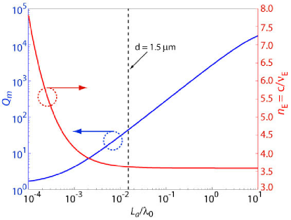
FDTD simulations to this point have approximated the metal contacts defining the MIM waveguide structures with perfect conductor boundary conditions, neglecting ohmic heating loss in the metal layers. Additionally, the optical losses within conventional THz QCLs include a contribution from free-carrier absorption, the level of which can be minimized through reduction of the thickness and doping levels of the semiconductor contact layersUnterrainer et al. (2002); Williams et al. (2003); Kohen et al. (2005). Given that the thin MIM waveguide structures studied here have a large fraction of mode energy at the metal surfaces, we will concern ourselves here with estimating the optical losses in the metal layers, with free-carrier absorption and other losses contributing at a level similar to that in conventional THz QCL structures. Incorporation of “real” metals into the 3D FDTD simulations would require a prohibitively large amount of memory and/or simulation time due to the very short skin depth at THz frequencies. Fortunately, an estimate of the ohmic heating losses in the metal can be obtained for the patterned MIM waveguide structure by considering the analytically tractable unpatterned MIM structure.
Specifically, we approximate the losses due to absorption in the metal contacts through an analysis of the fundamental, even parity, coupled-surface-plasmon mode in a simple planar 1D double-metal waveguide structurePrade et al. (1991). The complex dielectric constant of the Au metal layers in the THz ( m) are taken from Ref. Ordal et al. (1983) (). The refractive index of the QC active region core (which is assumed to be homogeneous and lossless) is taken to be 3.59. The fields and complex propagation constant are determined through numerical solution of the dispersion relation. The imaginary part of the propagation constant, which determines the modal loss per unit length down the waveguide (see Table 3), is converted to a loss per unit time and related to an effective due to metal absorption for comparison with the radiation losses plotted in Fig. 13:
| (4) |
where is the global energy velocity of the mode in the waveguide and the angular frequency of the mode. The energy velocity is computed from
| (5) |
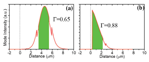
where is the time-averaged Poynting flux, the time-averaged energy density valid for a lossy, dispersive medium Ruppin (2002), and the quantities are integrated along the transverse width (-direction) of the waveguide. Fig. 14 shows the variation of and versus the width of the core region. This behavior is due to the penetration of the electric field into the lossy metallic layers when the active region is made thinner Williams et al. (2003); Maier (2006). The metal-absorption-limited propagation loss per unit length () and -factor () for active core region thicknesses of , , , , and m are tabulated in Table 3 along with the effective mode volume data. From this estimate we see that metal absorption loss will dominate the in-plane radiation losses of the -dipole-like mode of Fig. 12 for defect cavities of periods or more.
In order to connect this work with that of more conventional THz QC laser structures and measurements, and to determine whether such thin double-metal waveguide structures are at all practical, one must relate the calculated -factors of Fig. 13 and Fig. 14 to per unit length exponential loss coefficients. The typical gains that can be achieved in THz QC lasers at m are Kohen et al. (2005). These values refer to modes whose energy velocity is approximately equal to the phase velocity of the bulk material. In thin metal waveguide structures the energy velocity of the plasmon mode can be much reduced relative to that for a mode in a thick waveguide structure (see the dispersion of Fig. 7(e)); however, for the MIM waveguide thicknesses considered here ( m) the energy and core phase velocity are nearly equal and the metal absorption loss coefficients, , of Table 3 can be directly compared to measured gain coefficients of conventional laser structures. Such comparisons indicate that for all but the thinnest waveguide structure ( m), laser action should be achievable.
V Conclusions
In conclusion, we have described photonic crystal guided wave structures tailored for quantum cascade lasers, in which a full TM photonic bandgap is present and lateral electrical injection is possible. Laser cavity designs in both the mid-IR and THz ranges of the electromagnetic spectrum were considered. We identified candidate defect modes for lasing, and calculated their mode profiles and -factors. In addition, we have shown that it is possible - under appropriate conditions - to implement high-contrast photonic structures via the sole patterning of the top metal layer in THz QC lasers featuring double-metal waveguides. Such photonic crystal structures are of particular interest for laser structures due to the negligible damage they introduce into the active semiconductor layers and their reduced fabrication complexity.
Acknowledgements
The authors thank F. Julien, C. Sirtori, and Y. Chassagneux for useful discussions. The work conducted at the Universite Paris-Sud was performed as part of an EURYI scheme award (www.esf.org/euryi), with additional support from the PICS program n.3417. The Caltech portion of this work was supported by an AFOSR MURI program in plasmonics (http://www.plasmonmuri.caltech.edu/) and a DARPA UPR program in optofluidics (http://www.optofluidics.caltech.edu/).
References
- Gmachl et al. (2001) C. Gmachl, F. Capasso, D. L. Sivco, and A. Y. Cho, Rep. Prog. Phys 64, 1533 (2001).
- Diehl et al. (2006) L. Diehl, D. Bour, S. Corzine, J. Zhu, G. H fler, M. Loncar, M. Troccoli, and F. Capasso, Appl. Phys. Lett. 88, 201115 (2006).
- Darvish et al. (2006) S. R. Darvish, S. Slivken, A. Evans, J. S. Yu, and M. Razeghi, Appl. Phys. Lett. 88, 201114 (2006).
- Williams et al. (2005) B. Williams, S. Kumar, Q. Hu, and J. Reno, Optics Express 13, 3331 (2005).
- Hofstetter et al. (1999) D. Hofstetter, J. Faist, M. Beck, and U. Oesterle, Appl. Phys. Lett. 75, 3769 (1999).
- Schrenk et al. (2000) W. Schrenk, N. Finger, S. Gianordoli, L. Hvozdara, G. Strasser, and E. Gornik, Appl. Phys. Lett. 77, 2086 (2000).
- Colombelli et al. (2004a) R. Colombelli, K. Srinivasan, M. Troccoli, O. Painter, C. Gmachl, F. Capasso, D. M. Tennant, A. M. Sergent, D. L. Sivco, , et al., Science 302, 1374 (2004a).
- Srinivasan et al. (2004) K. Srinivasan, O. Painter, R. Colombelli, C. Gmachl, D. Tennant, A. Sergent, D. Sivco, A. Cho, M. Troccoli, and C. F, Appl. Phys. Lett. 84, 4164 (2004).
- Joannopoulos et al. (1995) J. D. Joannopoulos, R. D. Meade, and J. N. Winn, Photonic crystals (Princeton University Press, Princeton, 1995).
- Vurgaftman and Meyer (2003) I. Vurgaftman and J. Meyer, IEEE J. Quan. Elec. 39, 689 (2003).
- Painter and Srinivasan (2003) O. Painter and K. Srinivasan, Phys. Rev. B 68, 035110 (2003).
- Painter et al. (1999) O. Painter, J. Vučković, and A. Scherer, J. Opt. Soc. Am. B 16, 275 (1999).
- Imada et al. (2002) M. Imada, A. Chutinan, S. Noda, and M. Mochizuki, Phys. Rev. B 65, 195306 (2002).
- Meade et al. (1993) R. D. Meade, A. M. Rappe, K. D. Brommer, and J. D. Joannopoulos, J. Opt. Soc. Am. B 10, 328 (1993).
- Schubert and Rana (2006) M. Schubert and F. Rana, IEEE J. Quan. Elec. 42, 257 (2006).
- Johnson and Joannopoulos (2001) S. G. Johnson and J. D. Joannopoulos, Opt. Express 8, 173 (2001), URL http://www.opticsexpress.org/abstract.cfm?URI=OPEX-8-3-173.
- Bahriz et al. (2006) M. Bahriz, V. Moreau, J. Palomo, R. Colombelli, D. Austin, J. Cockburn, L. Wilson, A. Krysa, and J. Roberts, Appl. Phys. Lett. 88, 181103 (2006).
- Colombelli et al. (2004b) R. Colombelli, K. Srinivasan, M. Troccoli, O. Painter, C. Gmachl, D. Tennant, A. Sergent, D. Sivco, A. Cho, and F. Capasso, IOP Nanotechnology 15, 675 (2004b).
- Raether (1988) H. Raether, Surface Plasmons, vol. 111 of Springer-Verlag Tracts in Modern Physics (Springer-Verlag, New York, 1988).
- Sirtori et al. (1998) C. Sirtori, C. Gmachl, F. Capasso, J. Faist, D. L. Sivco, A. L. Hutchinson, and A. Y. Cho, Opt. Lett. 23, 1366 (1998).
- Yeh (2005) P. Yeh, Optical Waves in Layered Media (John Wiley and Sons, 2005).
- D’Urso et al. (1998) B. D’Urso, O. Painter, J. O’Brien, T. Tombrello, A. Scherer, and A. Yariv, J. Opt. Soc. Am. B 15, 1155 (1998).
- Srinivasan and Painter (2002) K. Srinivasan and O. Painter, Opt. Express 10, 670 (2002).
- Unterrainer et al. (2002) K. Unterrainer, R. Colombelli, C. Gmachl, F. Capasso, H. Hwang, A. Sergent, D. Sivco, and A. Cho, Appl. Phys. Lett. 80, 3060 (2002).
- Williams et al. (2003) B. Williams, S. Kumar, H. Callebaut, Q. Hu, and J. Reno, Appl. Phys. Lett. 83, 2124 (2003).
- Prade et al. (1991) B. Prade, J. Y. Vinet, and A. Mysyrowicz, Phys. Rev. B 44, 13556 (1991).
- Mahler et al. (2005) L. Mahler, A. Redicucci, R. Khler, F. Beltram, H. E. Beere, E. H. Linfield, and D. A. Ritchie, Appl. Phys. Lett. 87, 181101 (2005).
- Demichel et al. (2006) O. Demichel, L. Mahler, T. Losco, C. Mauro, R. Green, J. Xu, A. Redicucci, F. Beltram, H. E. Beere, D. A. Ritchie, et al., Opt. Express 14, 5337 (2006).
- Maier (2006) S. Maier, Optics Express 14, 1957 (2006).
- Kohen et al. (2005) S. Kohen, B. S. Williams, and Q. Hu, J. Appl. Phys. 97, 053106 (2005).
- Mur (1981) G. Mur, IEEE Transactions on Electromagnetic Compatibility 23, 377 (1981).
- Pendry et al. (2004) J. B. Pendry, L. Martin-Moreno, and F. J. Garcia-Vidal, Science 305, 847 (2004).
- (33) O. Painter and R. Colombelli (????), manuscript in preparation.
- Ordal et al. (1983) M. Ordal, L. Long, R. Bell, S. E. Bell, R. R. Bell, R. Alexander, and C. A. Ward, Applied Optics 22, 1099 (1983).
- Ruppin (2002) R. Ruppin, Phys. Lett. A 299, 309 (2002).
- Johnson et al. (1999) S. G. Johnson, S. Fan, P. R. Villeneuve, J. D. Joannopoulos, and L. A. Kolodziejaki, Phys. Rev. B 60, 5751 (1999).