A Vertex Trigger based on Cylindrical Multiwire Proportional Chambers
Abstract
This article describes the technical implementation and the performance of the -vertex trigger (CIP2k), which is part of the H1-experiment at HERA.
The HERA storage ring and collider was designed to investigate electron (and positron) proton scattering at a center-of-mass energy of 320 GV. To improve the sensitivity for detecting non-standard model physics and other high momentum transfer phenomena, the HERA ring has been ugraded between 2000 and 2003 to increase the specific luminosity for the experiments. In order to cope with the increased event and background rate the experiments were upgraded, too. The CIP2k trigger system is based on a set of five cylindrical multiwire proportional chambers with cathode pad readout, and allows to distinguish between events induced by beam background and -interactions at the first trigger stage. The trigger decision is calculated dead-time free with a latency of 1.5 s in parallel to the beam clock at 10.4 MHz. The trigger-logic is realized in large field programmable gate arrays (FPGA) using the hardware description language Verilog. The system is operational since October 2003. It suppresses background events with high efficiency and provides event timing information, as designed.
keywords:
FPGA , ASIC , MWPC , Trigger , H1 , HERA, , , , , , ††thanks: Present address: DESY, D-22607 Hamburg, Germany , , , , , , ††thanks: Present address: Philips Medical Systems DMC GmbH, D-22335 Hamburg, Germany , ,
, ††thanks: Present address: Continental Teves AG & Co., oHG, D-60488 Frankfurt, Germany , ††thanks: Present address: GSI, D-64291 Darmstadt, Germany
,
1 Introduction
During the period 1993-2000 each of the two experiments at the HERA collider, H1 and ZEUS, collected an integrated luminosity of approximatly 100 (HERA I run). The subsequent upgrade of the accelerator lead to a significantly increased specific luminosity in 2004, namely cm-2s-1mA-2 three times higher as compared to HERA I. The target for the integrated luminosity is per year. This was achieved by increasing the proton beam current and by reducing the beam cross sections at the interaction point (IP). The latter required the installation of strong superconducting focussing magnets inside the H1 experiment [1] close to the IP, which allow an early separation of the electron and the proton beam. The new beam parameters are listed in Table 1 in comparison to those of HERA I.
| HERA I | HERA II | ||
|---|---|---|---|
| Electron (positron) current | [mA] | 50 | 55 (35) |
| Proton current | [mA] | 100 | 135 (105) |
| Interaction focus | [] | ||
| Specific luminosity | [cm-2s-1mA-2] |
The change of the beam optics led to significantly increased beam induced background in the experiment, whose separation from interaction as fast as possible is crucial for efficient data taking. In the H1 experiment the corresponding event-by-event trigger decision is based on timing or on the reconstructed vertex position using fast drift or multiwire proportional chamber data. In HERA I running a trigger based on the information of two sets of two cylindrical multiwire proportional chambers (central inner (CIP) and central outer (COP) MWPC) was used for this purpose [2, 3]. It reconstructed the vertex position along the beam axis within 30 cm around the IP and delivered an event timing. This information was part of most H1 trigger decisions.
To cope with the high background rate the central inner proportional chambers of the H1 experiment and the trigger based on their signals were redesigned to allow reconstruction of the vertex position over a range of 3.5 m along the beam axis (-vertex). With increased acceptance beam induced background can be more efficiently rejected.
The construction of the new central inner proportional chamber, the design and the implementation of the -vertex trigger derived from it, and the performance of the complete system are described in this article.
1.1 Background situation
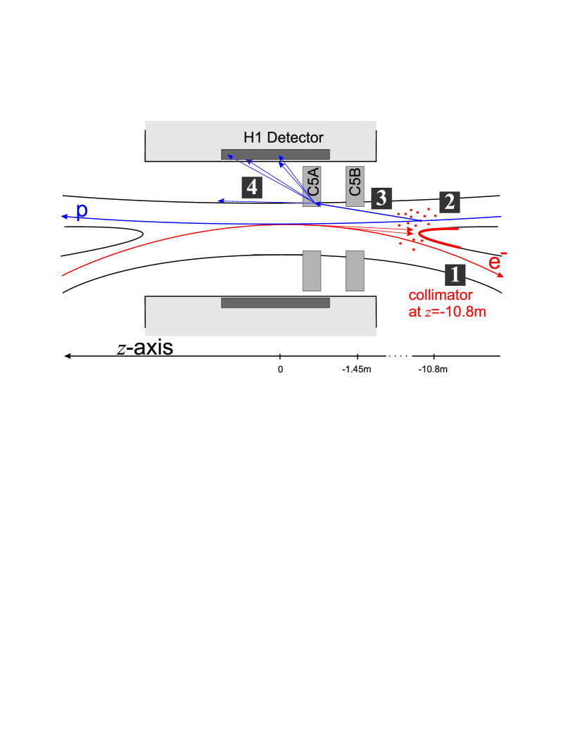
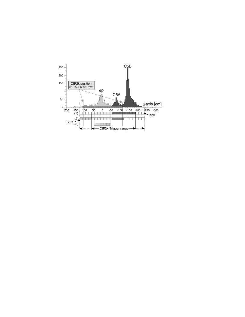
The deflection of the electron beam induced by the strong focussing magnets near the interaction point creates a high level of synchrotron radiation of about 100 kW intensity. The interaction region is designed such that most of this synchrotron radiation is absorbed far away from the experiment. The closest absorber for synchrotron radiation is located at m, i.e. 10.8 m away from the IP111At the H1 experiment, the -axis points along the proton flight direction, the -axis points towards the center of the ring, the -axis in the upward direction. The origin of this right handed Cartesian coordinate system is the nominal interaction point of the H1 experiment. The azimuthal angle in the -plane is . The polar angle is (positive , ). The parts of the detector with positive (negative) coordinates are often referred to as the forward (backward)regions.. A small fraction of the synchrotron radiation is reflected back rather than being absorbed. Two collimators in the beam pipe (C5A at cm and C5B at cm) protect the H1 detector against this backscattered synchrotron radiation. The setup is depicted in Fig. 1. The synchrotron radiation leads to increased rest-gas pressure in the beam pipe close to the absorber at m, and consequently the rate of collisions of protons with the gas molecules is high. In these beam-gas interactions off-momentum particles are produced creating hadronic showers through secondary interactions in the collimators, and high particle multiplicities in the tracking detectors. At HERA II this mechanism is the dominant source of beam induced background [4].
In order to use the high luminosity provided by HERA II efficiently the fraction of background events has to be suppressed at an early stage of the trigger. Due to the fixed bandwidth of the H1 data acquisition system, it is mandatory to identify these interactions without causing any interruption of data taking. Each event which is not filtered out at the first level of the pipelined trigger system causes deadtime.
1.2 Background identification
Background events can be identified if their origin along the beam axis (-vertex) is known. This is obvious from inspecting Fig. 9 in Sec. 3.1.3, which shows the reconstructed -vertex distribution observed in a typical HERA II run. Beam induced background events originating from the collimators C5A and C5B and -interactions can clearly be distinguished. The CIP2k -vertex trigger system was therefore developed to reconstruct the trajectories of charged particles coming from interactions near the beam axis. It determines the vertices and creates a corresponding histogram for each bunch crossing. Event signatures with most of the tracks pointing to the backward region are rejected by the trigger.
The track reconstruction is based on data from a set of five cylindrical multiwire proportional chambers (central inner proportional chambers: CIP2k) with cathode pad readout. As the name indicates the CIP2k encompasses the interaction region in the center of H1 detector. It has a total of 8480 readout pads, providing space points and timing information. Each layer is equally subdivided into 16 azimuthal segments in with approximately 20 mm wide segmentation along the beam axis. The chamber has sufficient granularity to resolve the event structure, even in high multiplicity events. Five layers ensure a high redundancy for the reconstruction with a negligible rate of combinatorial background. Operation of the trigger system remains efficient even if one or two layers of the chamber are not operational. Simulation studies were done beforehand in order to optimize the granularity of the chamber and to determine the expected redundancy and background rejection power[5, 6]. Since multiwire proportional chambers are characterized by a response time below 10 ns [7], the CIP2k -vertex trigger delivers accurate event timing () with optimal efficiency.
All H1 detectors and trigger systems store their information for 32 bunch crossings (3.1 s) [1]. The level 1 (L1) trigger decision starts the readout after 2.3 s, hence all L1 signals have to be delivered not later than 2 s. The decision has to be made for every bunch crossing. Thus all pads have to be read out within 96 ns, corresponding to the bunch crossing frequency of 10.4 MHz. In the CIP2k trigger system this requirement is met using large field programmable gate arays (FPGA) both for the trigger decision and the storage of the event data for readout by the data acquisition system.
2 Multiwire proportional chamber
2.1 Construction
The construction of the CIP2k in the University of Zürich shops followed closely that of a thin cylindrical proportional chamber with cathode pad readout [2] which was installed in H1 during the HERA I run. This chamber also delivered signals for a -vertex trigger [3] and ran very stable and efficiently over the whole data taking period of HERA I.
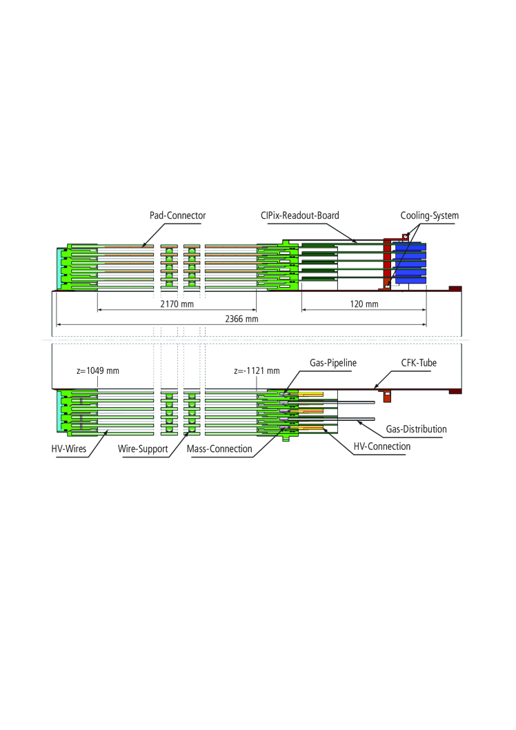
The cylindrical chamber has five radial layers with an inner radius of 154 mm and an outer radius of 196 mm and an active length of 2170 mm. The total length of the chamber 2366 mm including end flanges and 120 mm for the electronics and the cooling. The chamber encloses the nominal interaction region and is mounted between the central silicon detector [8] on the inside and the central drift chamber (CJC) [1] on the outside. The active region extends from =-1121 mm to =1049 mm, corresponding to an angular acceptance . Figure 2 shows a cross section of the chamber. All necessary details for the construction techniques and the choice of materials are given in ref. [9].
The sandwich-like construction of each radial layer shown in Fig. 3 was chosen in order to keep the material budget low without compromizing on stability and robustness.
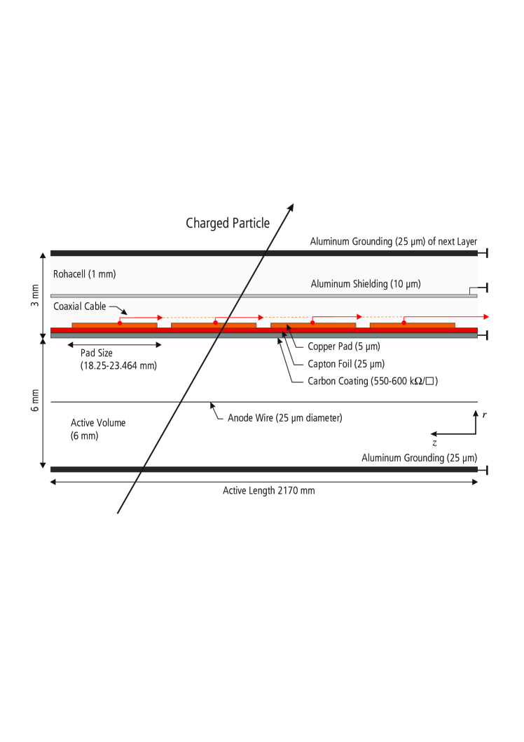
Each layer contains 480 gold-plated tungsten anode wires, 2 mm spaced, with a diameter of 25 m and mounted in a gas volume of 16 liters. They are kept at a voltage between 2250 and 2500 V. At the outer layers a lower voltage is needed, since electric field on the wire is higher. The wires are supported by epoxy rings at one and two thirds of the chamber length. A 3 mm gap separates the anode from the cathode planes, which consist an aluminum foil (25 m thickness) on the inner and a carbon coated capton foil on the outer side. The charge collected on the anode wires induces a charge on the high resistivity cathode planes (550-600 k) and a signal on the copper pads on the outer side of the capton foil. Copper was chosen as pad material instead of aluminum as in the original central inner proportional chamber [2], because a large fraction of the induced signal was lost in the latter case where the pad thickness was smaller than the skin depth. Furthermore the signal transmission was improved by using miniature coaxial cables [10, 11] with very low dielectric and inductive coefficients to transport the induced charge ( electrons) of each pad to a connector at the rear end flange of the chamber. These cables are embedded in groves in the layer of Rohacell [12] (thickness 1mm), which backs the foils and guarantees for the mechanical stability. Each pad covers 22.5∘ in azimuth. In -direction, the size and number of pads vary at each layer as described below.
2.2 Pad geometry
The arrangement of the pads is optimized for a simple trigger algorithm. While the pad size is constant within each layer along , it increases proportional to the distance from the beam axis from 18.25 to 23.464 mm (projective geometry). The innermost pad size was dictated by the requirement that two pads taken in a logical OR match the granularity of the previous set up [3]. The pads are arranged such that tracks from the same vertex generate similar patterns independent of , as described in Sec. 3.1. Every 328.50 mm the pads of the five layers are exactly aligned above each other. This distance equals two bins in the -vertex histogram. In total, there are 8,480 pads in 16 -sectors (see Table 2).
| Layer | 0 | 1 | 2 | 3 | 4 |
| number of pads in | 119 | 112 | 106 | 99 | 93 |
| total number of pads | 1904 | 1792 | 1696 | 1584 | 1488 |
| length of pad [mm] | 18.250 | 19.323 | 20.531 | 21.900 | 23.464 |
| length of last pad [mm] | 16.0 | 19.323 | 13.74 | 21.900 | 10.8 |
| anode radius [mm] | 157 | 166 | 175 | 184 | 193 |
| spacing of wires [mm] | 2.06 | 2.17 | 2.29 | 2.41 | 2.53 |
2.3 Gas system and high voltage distribution
The chamber is operated with a gas mixture of argon (49.9%), isobutane (49.9%) and freon (0.2%). The gas flow is controlled by the H1 wide gas control system [1]. Two independent closed loops supply the five layers. The static pressure of the chambers relative to atmospheric pressure is regulated to be within bar. This ensures that the active gap in the chamber is not distorted. Since the tracking detectors are surrounded by a N2 atmosphere, contamination with N2 through leakage and other changes in the gas mixture are monitored constantly in order to avoid changes in the gas amplification.
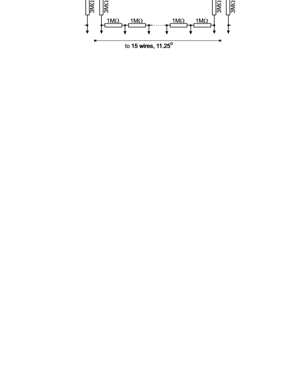
The 480 anode wires of each layer are grouped into 32 sectors of 15 wires. Each group is connected to a high voltage cable via 3.3 M resistor, while the anode wires are connected to their neighbours with a 1 M resistor. This allows a high voltage degrading in case of a short circuit in one region of the chamber with minimal efficiency loss [14]. An illustration of the high voltage distribution is given in Fig. 4.
2.4 Front end electronics
The pad information is transferred to the front end electronics via a 120-pin connector on the chamber. Sixteen connectors per layer transmit the signals of all pads along of one -sector. The front end electronics consists of 80 highly integrated readout boards with a size of in 12-layer printed circuit board (PCB) technology. They were developed at the Paul Scherrer Institut. Each board covers one -sector and contains two application specific integrated circuits (ASIC) especially developed for the readout (called CIPix) and two 17:1 multiplexers [15]. The information of one double layer is sent via an optical fibre to the receiver cards 40 m away in the electronics trailer of the experiment.
2.4.1 The CIPix readout chip
Each CIPix readout chip has capacity for 64 analog inputs, of which up to 60 are used while the remaining serve testing purposes. The CIPix readout chip was developed at the ASIC laboratory of the University of Heidelberg in a 0.8 m CMOS-process. Figure 5 shows the block diagram of one CIPix chip. Each of the 64 analog input channels consists of:
-
•
A charge-sensitive preamplifier with a gain of 20 mV per electrons. The preamplifier characteristics are programmable.
-
•
An analog signal shaping to a CR-RC semi-Gaussian pulse with programmable shaping times.
-
•
Digitalization by a one-bit comparator with programmable threshold and polarity. The digitized information is synchronized to the 10.4 MHz beam clock signal.
The digitized pad information is multiplexed fourfold into 17 digital channels (15 outputs and two control channels) at 41.6 MHz in each CIPix. In parallel, one analog output channel is provided, which can be used to monitor any of the 64 input channels. The first of the four multiplexed pads is tagged, and hence allows a synchronization with the demultiplexing electronics in the trigger system. All boards of one layer are interconnected by an bus daisy-chain. This allows to set all programmable parameters layer-wise and a serialized temperature measurement [16]. The system itself is controlled by the experiment control system PVSS II [17, 18].
2.4.2 Readout board, optical link and cooling
Figure 6 provides an overview of the electronics on the chamber, while Figure 7 contains details of the front end PCB. The 15 plus 2 output channels of a CIPix are multiplexed to one output signal per CIPix and transmitted to an optical link system [19]. Pairs of adjacent boards are interconnected by a flexible strip-line on a capton foil carrier. One of the PCBs holds the optical link system while the other one holds the interface and the voltage regulators. They are powered from the electronics trailer. The overall synchronisation is done with the global HERA clock signal. It is the input for a low jitter phase-locked loop which generates the 41.6 MHz clock. The latter is delivered to the 17:1 multiplexers and in addition to the HERA clock to all four CIPix chips.
Since only optical transmission can support the high rates with low cross talk and a minimal power consumption, an optical link between the on-detector electronics and the receiver cards was developed by ETH Zürich based on optical hybrids which do the electro-optical conversion [19]. These hybrids have six sender and two receiver diodes for the 10.4 MHz HERA clock. For redundancy two HERA clock signals are transmitted in parallel. The six senders transfer four digital data channels - one for each CIPix - with the signals of two sectors and two analog channels - each shared by two CIPix - to the readout system. All the light guides from one transmitter unit are bundled into a single cable.
The front end boards are cooled by direct contact to copper blocks which are connected to an outer and an inner cooling ring above and below the readout electronics. Both rings are water-cooled. The cooling of the boards is critical, because excessive heating may destroy the bond wires, which connect the readout ASIC to the board. Moreover, the connections within the 12 layer PCB could also suffer.
3 Trigger
The CIP2k trigger electronics serves two purposes:
-
•
It uses the chamber information of all 8,480 pads to deliver trigger information for each bunch crossing to the H1 central trigger.
-
•
It stores all the chamber information in a pipeline and delivers it to the H1 storage system in case of a positive trigger decision.
3.1 Trigger algorithm
A pipelined trigger algorithm has been developed which is divided into five steps [20]:
-
1.
Trackfinding
-
2.
Assembly of the -vertex histogram
-
3.
Histogram analysis
-
4.
Collection of information from the -sectors.
-
5.
Trigger decision
The first three steps are done in parallel for every -sector in the trigger cards, the summation in step four in the sum cards, and the final trigger decision in the master sum card. The algorithm has been implemented in APEX 20k400 FPGAs [21], is written in the hardware description language Verilog and made use of the development environment Altera Quartus (see ref. [20] for details).
3.1.1 Track reconstruction:
The information coming from the receiver cards is fed into the FPGAs of the trigger where it is first demultiplexed four times. Pads known to be defect may be permanently switched off or on in a filter module. At every startup of the trigger system, a list of defect pads is updated via the VME bus. In a second step valid track patterns with hits in at least four chamber layers are searched for. The projective geometry of the chamber simplifies this task, since a given -position leads to a unique pattern of pads showing hits in the five layers. This is illustrated in Fig. 8. To allow for local inefficiencies the corresponding -position of the track is stored even if a pad in a pattern is missing. The valid patterns are predefined in the local environment (LE) of every pad in the central layer. Each possible track pattern in the LE then points to a given -bin. Since 22 -bins are defined there exist 22 valid patterns in each LE.
3.1.2 Assembly of the -vertex histogram
For each -bin at total of 106 tracks can be identified corresponding to the number of pads in layer 2 and hence to the number of LEs. If a track is identified in the trigger module it is written into a 106 bit wide hit vector, defined for each of the 22 -bins. The tracks in the hit vector are counted for each bin in the adder module, which uses a major part of the FPGA logic because possible tracks have to be checked and summed up. The result is evaluated in less then two bunch crossings ( ns) in a cascade of adders, which counts the tracks in the hit vector in six steps (144 ns). Only 15 consecutive bins out of 22 are used for the trigger decision, corresponding to 1590 possible tracks. They represent the -vertex histogram for one -sector, calculated in one trigger card. The selection of the 15 out of 22 bins is programmable in the range cm (see Fig. 9). For monitoring purposes, the histogram is stored in a pipeline and can be read out via the VME bus together with the chamber information of the event.
3.1.3 Histogram analysis
For the trigger decision the bins of the -vertex histogram are grouped into a forward, a central and a backward region. This selection is programmable as shown in Fig. 9 for two examples. The configuration adapted to event fixes the backward region of the trigger to the range cm and the central region to cm. The second example concerns the cosmic muon trigger which requires coincidences between two quadrants.
3.1.4 Summing
Once the number of tracks in the three regions of each -sector is known, they are added in two consecutive steps to give a global, independent track distribution. The information of four -sectors is added first in the pre-sum card to yield -vertex regions for the four quadrants of the CIP2k chamber. The number of tracks of the quadrants is then added to get the global -regions in the main sum card. To keep the number of transfer cables to a reasonably low level, the number of tracks is limited to 255 in each region.
3.1.5 Trigger decision
A trigger decision is made by analyzing the track information in the forward, central and backward region based on global track information of each event in the pipeline. A precise timing information is evaluated (t0, 1 bit). It is set, if at least one track in the central region is identified by the -vertex trigger. To analyze the quality of the -event, the number of tracks identified in all three regions (4 bits) and the ratio between the number of central tracks and backward tracks (2 bits) is given to the central H1 trigger control. Up to 16 trigger elements (bits) [20] may be defined. They are transferred to the central trigger system for every event.
3.2 Trigger electronics
Seven crates house the trigger hardware: four trigger crates (TCr), one sum (SCr), one komposti ( internal label) and one subsystem trigger control (STC) crate [22]. Figure 10 provides an overview of the trigger electronics.
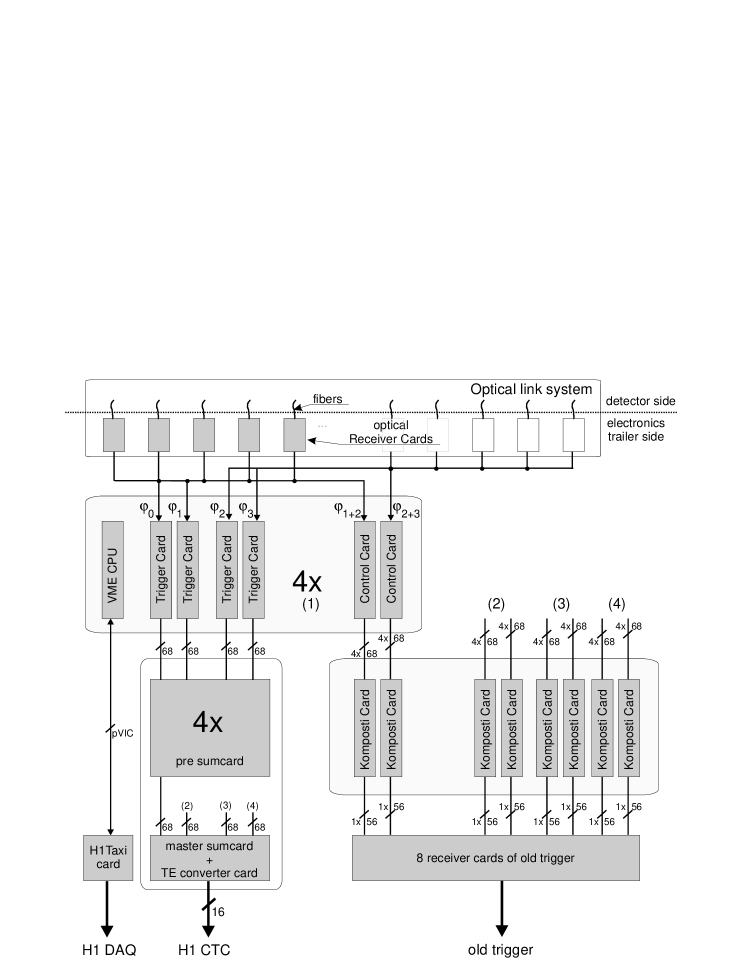
3.2.1 Trigger crates:
Each trigger crate hosts ten receiver (RC), four trigger (TC) and two control cards (CC) as well as one VME CPU. The crates have a special backplane and additional power supply units for 3.3 V and -5 V [23].
Each optical fiber originating from the CIPix PCB ends in a receiver card, which collects the information of four CIPix units, converts the optical signals to electrical signals and performs the 1:17 demultiplexing step. A clock signal, phase-locked to the HERA clock, is also generated here. The pad and clock signals are sent to the P2-backplane of the trigger crate [19]. This backplane was specially developed at the University of Heidelberg [24] to cope with the high number of chamber signals. Ten 96-pin three-row connectors are needed. The signals of a group of five RCs are linked into two trigger cards on the front side. Each trigger card deals with the information of all five layers of one -sector. A control card serves each pair of trigger cards and the five receiver cards linked to it with the control signals and extracts the pad information of the two innermost layers to the old -vertex trigger system [3]. The control card also contains hardware to monitor and control the relative phases of the clock signals.
The trigger card contains both the logic of the trigger algorithm and the storage pipeline for the chamber data of one -sector. In total 16 trigger cards are needed to process the complete chamber information, distributed across four crates. The trigger card, realized as an 8-layer PCB, was designed in cooperation with University of Heidelberg [24]. Each trigger card contains two Altera FPGAs [21], mounted in a ball grid array technique onto the PCB. The board is equipped with a 5 V to 1.8 V power converter to deliver the 1.8 V FPGA kernel voltage. External 3.3 V and 5 V power supplies are needed for the FPGA I/O pins and the VME bus and the IsPL [27] who controls it (see Fig. 11). Six EEPROMs [25], three for every FPGA contain the configuration code, three for every FPGA.
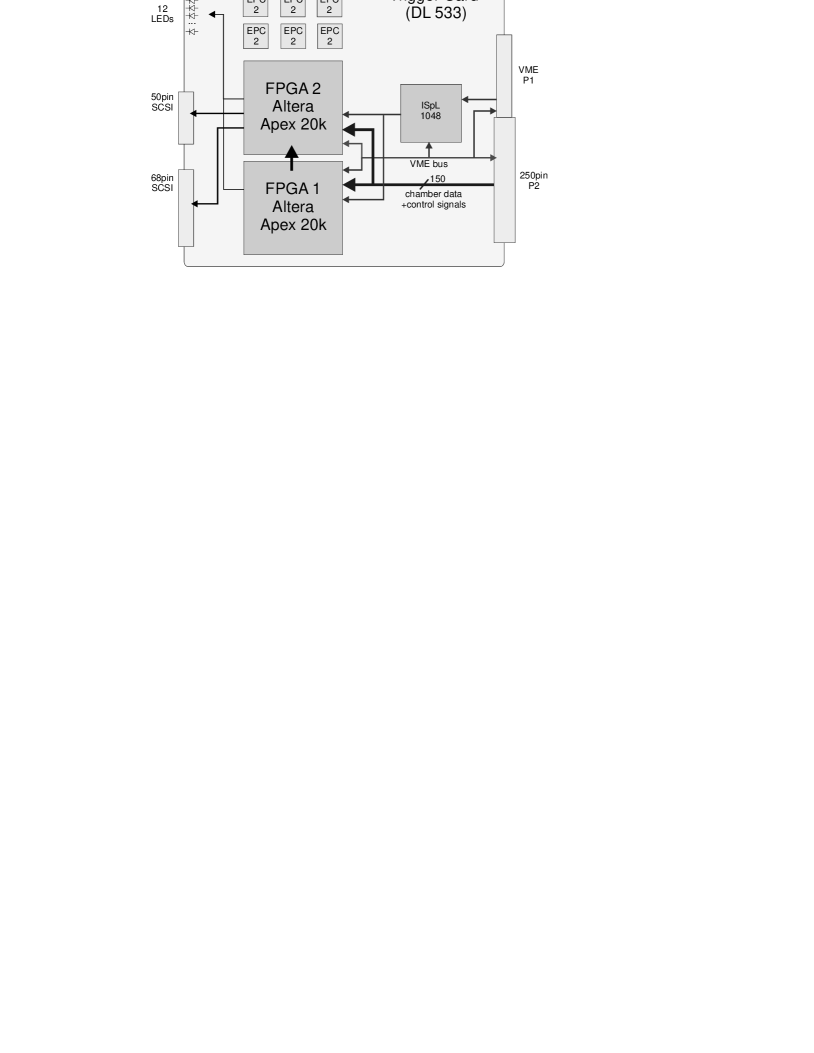
To transport the chamber information from the 250-pin input connector on the trigger card to the FPGAs 150 lines are needed. The trigger algorithm is distributed over two FPGAs, because one does not suffice for a complete -sector. Every FPGA deals with the information of 60 pads of five layers ( multiplexed channels). Tracks that point to pads of both CIPixes define the overlap area, known to both FPGAs. A 90 line interconnect bus connects both FPGAs. Information evaluated by FPGA I is transferred to FPGA II. FPGA II is connected to two SCSI-connectors to deliver -based data to the sum cards via LVDS converters [26], which transform the 3.3 V FPGA output (LVTTL, low voltage TTL) to a LVDS (low voltage differential standard) signal.
Every trigger card is equipped with a 32-bit VME bus controller residing in an in-system high density programmable logic device (IsPL) [27]. The 24-bit standard non-privileged address mode is used. 32 bidirectional data lines are linked to both FPGAs and to the ISpL, which is set up as a VME-bus slave unit and organizes the data transfer from the FPGAs to the VME bus master.
The pad information of the chamber is stored in a ring buffer (pipeline) 32 bunch crossings deep. Each trigger card provides the information of one -sector. In case of a positive level 1 trigger decision, data taking stops and the readout of the triggered event is organized. Five bunch crossings around the expected -event are read out. It takes 20 VME read cycles to read out one BC of one TC, 320 cycles per BC in total [20].
3.2.2 Summing crate
The trigger information of each trigger card is transferred to the summing crate (VME 21-slot 64x [23]). Here all 16 sectors are combined and a trigger decision is calculated. Five identical sum cards are used to perform this task. Four cards receive the information of four trigger crates each and combine it for a quadrant (pre-sum card, see Fig.10). The fifth card, the main sum card, combines everything and distributes the decision (the trigger elements (TEs)) to the H1 central trigger control (CTC). For monitoring, inputs and output signals of each sum card are read out.
The sum card was also developed in cooperation with University of Heidelberg [24], and is built around a single FPGA and an ISpL for configuration and VME bus service. The sum card is equipped with a 32-bit VME bus (6 address bits in a 16-bit mode, AM 0x29). For the configuration of the FPGA, three EEPROMs [25] are used. Each sum card is equipped with six SCSI connectors (five 68-pin and one 50-pin micro sub-D). The signal levels meet the LVDS standard. Each 68-pin connector transfers 32 single channels; the 50-pin connector transports 24 channels. In Figure 12 the sum card design is shown in a schematic view.
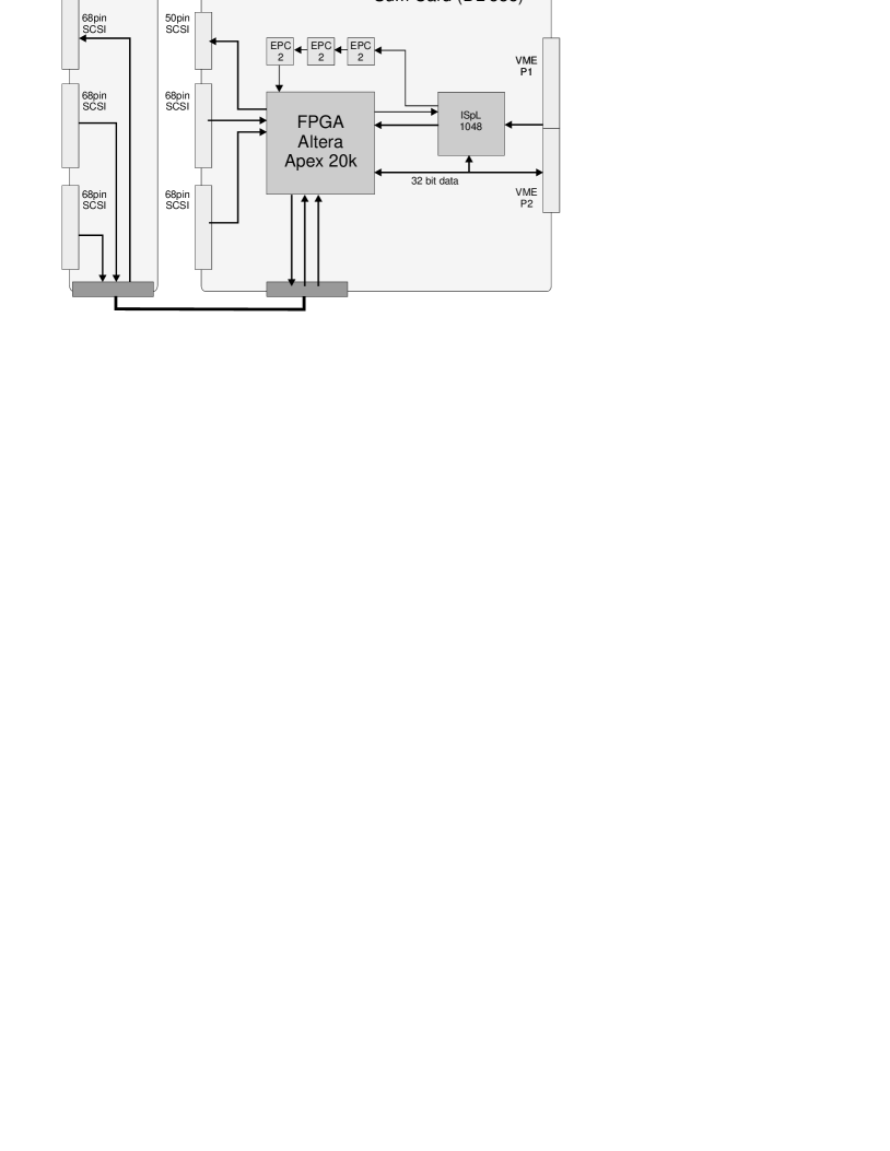
Each sum card has a piggy back board to cope with the large number of signals, which are processed in the sum card. Three 68-pin SCSI connectors are mounted on the piggy back board and are connected to the FPGA. The SCSI connectors can be used as input or output channels, depending on the LVDS converter/driver chip [26]. The master sum card receives the signals from the four pre-sum cards by four 68-pin input connectors, the trigger decision is provided on the 50-pin output connector.
3.2.3 Komposti crates
The komposti crate (VME 21-slot [23]) holds eight komposti cards, which use the same hardware as the sum card, but differ in the programming of the FPGA. The komposti card demultiplexes the data of the two innermost layers (120 pads of layer 0 and 1 of two -sectors) and merges it to 56 output signals provided at the two output SCSI connectors. Four pads of the new chamber are merged to one input channel for the old trigger system [3]. The merged data is linked into 8 passive (without power supply and active electronic elements) converter cards that form the LVDS signal of the komposti card to a pseudo-analog differential input signal in two 50-pin connectors. Together with the pad information of the two layers of the outer proportional chamber (COP), the old -vertex trigger can be used in a 3-out-of-4 layer option [3], since the information of layer 0 and layer 1 is combined at the komposti card (logical AND).
Running the old trigger in parallel was demanded because it entailed a threshold cut on the transverse momentum of a track GV/, had a finer resolution, and it also served calorimeter trigger towers.
3.3 Data acquisition
The CIP2k DAQ system consists of four VME CPU processor boards [28], which communicate with the trigger cards, do the initial setup of the trigger-system and read out the stored chamber information from the ring buffer in the FPGA. Each CPU reads the data of four sectors. The CPU and the trigger card communicate via the VME bus, using single cycle D32/A24 access. The CPUs are interconnected by a PCI vertical interconnect bus system [28].
Once the H1 central trigger decides to keep an event, all four CPUs start the readout simultaneously, triggered by high priority interrupts. The readout time is dominated by reading the pad data of five time slices from the VME bus. Using the pVIC bus the information from all sectors is collected on a single crate. This synchronous part of the readout ends after 1 ms, as required for H1 data acquisition systems. 16 buffers are available at this stage, in order to avoid possible second order deadtime effects caused by trigger bursts. The asynchronous part of the readout operates on these buffers. It starts with a data reduction reduction process on the main CPU. The chamber data, which are stored as bit patterns, are translated into 16-bit wide pad numbers, resulting in an effective zero suppression if the occupancy of the chamber is less than 10 %. During this process, pads that are known to be bad are removed from the data. Identical filters are applied during the trigger algorithm in order to ensure consistency of data and trigger. The data are then transferred by the VME bus to the H1 central data acquisition system [29].
3.3.1 Control system
An -bus [33] based system was developed to program the registers of the CIPix [16]. The system is controlled by an 8-bit microprocessor (pic16F877) that is addressed via a RS232 serial port connection. The programming of the CIPix settings is done by a Linux-based PC, installed in the H1 control room with a 25 m long RS232 cable connection to the -bus micro controller in the electronics trailer (CIPix-trailer-box).
Moreover, a temperature control system was developed, using a (separate) one-wire-bus [32], which is connected to a temperature measurement chip on each CIPix board at the detector. This chip is connected to a second serial port of the CIPix-trailer-box and sends the measured temperatures to the CPU in the komposti crate, The VME CPU receives the actual temperature and sends a continuous signal to a watch dog card. In case of high temperature or any other failure this signal stops and the watchdog switches off all CIPix board power supplies.
4 System performance
The CIP2K trigger system is fully operational since autumn 2003. Some basic performance tests of the new chamber and trigger electronics will be presented in this section. The comparisons presented below are all based on particle trajectories reconstructed in the central jet chamber (CJC). The spatial resolution of the CIP2K chamber and the trigger timing as well as single pad efficiencies are studied with muons from cosmic rays, trigger efficiencies with data.
4.1 Spatial resolution
Events with cosmic muons are selected to determine the spatial resolution. These events consist of two track halves, reconstructed in opposite sides of the CJC. The two track halves are constrained to have common track parameters, which improves the CJC position measurement significantly. Figure 13 shows the difference in between the track position extrapolated to the CIP2K wire plane and the center of the active pads in the corresponding azimuthal sector for three layers.

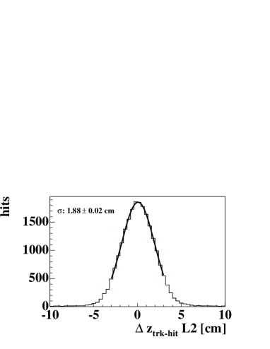
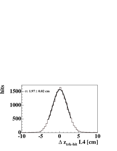
The RMS-width of the distribution is , and . This is in good agreement with the expected width, dominated by the finite pad size and the resolution of the CJC chamber. The chamber noise is negligible, as there are virtually no entries outside .
4.2 Trigger timing
The trigger timing is studied using the event sample with cosmic rays. Since the muons are not synchronized to the HERA beam clock it is possible to reconstruct the time resolution of the CIP2K system. The events are triggered by the drift-chamber trigger [31], which has only a moderate time resolution (). Figure 14 shows the CJC event time for events with the CIP2K T0 trigger active.

The CJC event time is the time at which the muon was closest to the axis. The time distribution is well described by the product of two threshold functions with the parameter for the intrinsic resolution of the CIP2K chambers and the electronics:
The width is found to be , well compatible with expectations from chamber and electronics design.
4.3 Chamber and trigger efficiency
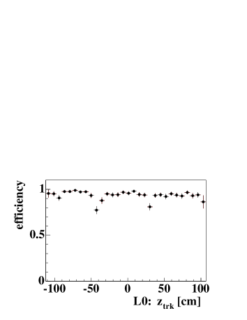
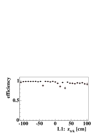
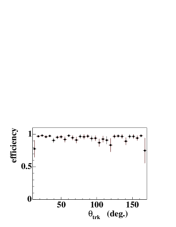
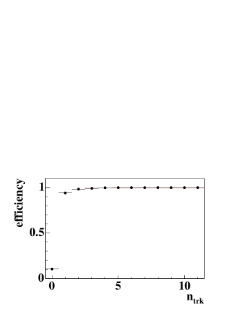
The chamber efficiency was also deduced from the muon sample. The tracks in this sample are predominantly produced at polar angles . They cover the full range along the axis. Figures 15(a) and (b) show the pad efficiency for all pads in one azimuthal sector in layer 0 and layer 1. Clearly visible is the reduced efficiency in both planes at and cm which corresponds to the position of the support rings for the anode wires. Figure 15(c) shows the trigger track efficiency which is measured with data as a function of the polar angle . For this study tracks are selected which are isolated in the CJC. A CIP2K trigger track requires a valid pattern with hits in at least four layers. The single-track trigger efficiency in events is better than in the muon sample, because most tracks in events have polar angles different from , so their average energy loss is higher. Furthermore, tracks passing the chamber at these polar angles may induce signals on several adjacent pads, again increasing the detection efficiency. The wire support structures are arranged far from the nominal interaction point, and their impact on the detection efficiency of tracks from collisions is not visible anymore. Lastly Fig. 15(d) shows the efficiency - the efficiency for finding a CIP2k track in the central region needed for event timing - as a function of the track multiplicity. For events with only one reconstructed track it is 95 %. This includes also inefficiencies due to broken readout electronics and HV problems.
4.4 Background discrimination
One of the main tasks of the CIP2K trigger system is the discrimination of events and high-multiplicity background events with displaced -vertex at the first trigger level. For many physics channels a veto condition is applied on the first trigger level, based on CIP2K signals. An example of a fairly soft veto condition is the following:
-
•
more than 100 tracks found in the CIP2K system
-
•
the number of tracks with reconstructed -vertex in the central region must not exceed the number of tracks with reconstructed -vertex in the backward region.
Two different event samples have been studied to monitor the performance of this veto condition. A minimum bias sample has been selected based on randomly triggered events, independent of any detector activity. Alternatively, the veto condition was studied for events triggered by a localized energy deposition in the liquid argon calorimeter (LAr electron trigger). Only those events are considered in the analysis with at least one good CJC track within the CIP2K acceptance. The CJC tracks are required to have a minimum of 20 detector hits, in order to ensure a good coordinate measurement. Since the -vertex reconstruction often fails for background events, the -vertex position of the primary interaction was estimated using the track with the largest number of hits. Events with tracks not pointing back to the same vertex within were excluded from the analysis. This removes events where the track reconstruction failed, but retains most events with multiple interaction vertices. Figure 16 shows the -vertex position as defined above for the minimum bias sample (top) and the sample triggered by the LAR trigger (bottom). The shaded histogram shows the events which are rejected by the CIP2K veto condition.

The minimum bias sample is dominated by background events, such as collisions of protons or electrons with gas molecules in the beam pipe. This is clearly visible in the vertex position histogram. The two peaks near and , correspond to the position of the collimators C5a and C5b, respectively. Secondary interactions of proton-gas interactions in the collimator produce events with high particle multiplicities. The flat distribution along mainly stems from electron-gas interactions. These events usually have low track multiplicities. No enhancement around the nominal interaction region at cm is visible. The background rejection by the -vertex trigger can be further improved if the high multiplicity cut of the veto condition is reduced. In combination with early signals from the backward scintillator veto wall [1] the rejection in the collimator region reaches values close to 100 %.
5 Summary
This publication describes the new five layer multi wire proportional chamber CIP2k with optical readout and a -vertex trigger system for the H1 detector at HERA II. The main purpose of the trigger system is the suppression of high multiplicity background events originating from the backward part of the detector at the first trigger level. After the luminosity upgrade of the HERA collider, the rate of such events has increased significantly. The new chamber with the -vertex trigger system is fully operational since autumn 2003. The trigger system is capable of reconstructing the -vertex position in parallel to the HERA beam clock at . The latency of the trigger decision is only . This was achieved by choosing FPGA technology for the track finding and histograming algorithms.
The performance of the new CIP2K trigger system was analyzed. The chamber behaves as expected in terms of spatial and time resolution. The single track trigger-efficiencies are close to %. The CIP2k trigger decision serves as the main time base for other track based trigger systems. A veto condition for rejecting background produced by secondary interactions in collimators in the vicinity of the interaction point was studied in greater detail. Such algorithms have become an integral part of the H1 trigger system, and help to keep the H1 data taking efficiency high.
References
- [1] I. Abt et al., Nucl. Instrum. Meth. A 386 (1997) 310; ibid. 348.
- [2] K. Müller et al., Nucl. Instrum. Meth. A312 (1992) 457.
- [3] S. Eichenberger et al., Nucl. Instrum. Meth. A323 (1992) 532.
- [4] V. Andreev et al., Technical Report on the Beam Induced Backgrounds in the H1 Detector, H1 note H1-IN-606 (10/2002).
- [5] A. Schweitzer, Optimierung eines -Vertex Triggers für den H1 Detektor bei HERA, Diploma thesis, Univ. Heidelberg (1999), see [6].
-
[6]
Theses related to this project are available at
http://www.physik.unizh.ch/groups/h1/publicationsmain.html - [7] F. Sauli, Principles of MWPC and Drift Chambers, CERN-Report 77-03, reprinted in T. Ferbel, Experimental Techniques in High Energy Physics, Menlo Park, USA: Addison-Wesley (1987) (Frontiers in Physics, 64).
- [8] D. Pitzl et al., Nucl. Instrum. Meth. A454 (2000) 334.
-
[9]
K. Bösiger, P. Robmann, and S. Steiner,
H1 CIP-Upgrade: 5-lagige Proportionalkammer, Physik-Institut,
Universität Zürich, internal report (1999), available at
http://www.physik.unizh.ch/groups/h1/text/CIP_peter.ps.gz - [10] Axon Kabel GmbH, Postfach 1131, D-71229 Leonberg, Germany
- [11] M. Kollak, Entwicklung einer Stripline-Auslese für Kathodensignale einer langen, zylindrischen Vieldrahtproportionalkammer, Diploma thesis, Univ. Heidelberg (1998), see [6].
- [12] Rohacell 51, Röhm (Schweiz) GmbH, CH-8306 Brüttisellen.
-
[13]
CAEN S.p.A., I-55049 Viareggio, Italy,
see http://www.caen.it/nuclear/index.php - [14] N. Werner, Measurement of the Charged Current Cross Section in Positron–Proton Collisions at HERA, PhD Thesis, Univ. Zürich, 2004, see [6].
- [15] Hewlett Packard HDMP 1032
- [16] A. Vollhardt, Entwurf und Bau einer Frontend-Steuerung für das CIP-Upgrade Projekt für H1 bei HERA, Diploma thesis, Univ. Heidelberg (2001), see [6].
-
[17]
H. Klehr, CIP2000 User Manual,
http://www.desy.de/ h1cip/documents/CIP2000_expertManual.ps -
[18]
ETM AG, PVSS II -process visualization and control system,
http://www.pvss.com/english/forschung.htm. - [19] S. Lüders et al., Nucl. Instrum. Meth. A484 (2002) 515.
- [20] M. Urban, The New z-Vertex Trigger for the H1 Experiment at HERA, PhD Thesis, Univ. Zürich (2004), see [6].
-
[21]
Altera 20K400E FPGA, Altera Corporation, San Jose, CA 95134,
USA: Description of the Altera APEX 20k device family,
http://www.altera.com/literature/ds/apex.pdf. - [22] M. Urban, J. Becker, S. Schmitt, and U. Straumann, Proc. IEEE 2002 Nuclear Science Symposium (NSS) and Medical Imaging Conference (MIC) and Symposium on Nuclear Power Systems, Norfolk, Virginia (2002), IEEE Trans. Nucl. Sci. 50 (2003) 903.
- [23] VME crates: W-IE-NE-R Plein & Baus GmbH, D-51399 Burscheid, Germany. http://www.wiener-d.com/SC/1/2.html
-
[24]
Electronics Workshop of the Physics Institute of
the University of Heidelberg,
http://pi1.physi.uni-heidelberg.de/physi/ew/Entwicklung.php. - [25] EEPROM (electrically erasable programmable read-only memory) EPC2-LC20, Altera Corporation, see [21].
-
[26]
3V LVDS quad CMOS differential line driver
DS90LV031/032,
Dallas Semiconductor, Dallas, Texas 75244, USA
http://www.datasheetcatalog.com/maxim-dallassemiconductor/1/ -
[27]
In-system high density programmable logic device
ispLSI 1048E, Lattice Semiconductor Corporation, Hillsboro, OR 97124, USA
http://www.latticesemi.com/ -
[28]
Creative Electronic Systems, CH-1212 Grand Lancy, Switzerland,
documentation of the RIO 8062 CPU and pVIC,
http://www.ces.ch/documents/documents.html. - [29] J. Becker, H. Cramer, M. Hildebrandt, K. Müller, S. Schmitt, U. Straumann, M. Urban, and N. Werner, Proc. 8th Topical Seminar on Innovative Particle and Radiation Detectors, Siena, Italy (2002), Nucl. Phys. Proc. Suppl. 125 (2003) 277.
-
[30]
M. Urban, Proc. Workshop on Electronics
for LHC and future Experiments, Boston, USA (2004),
http://lhc-workshop-2004.web.cern.ch/lhc%2Dworkshop%2D2004/ - [31] T. Wolff et al., Nucl. Instrum. Meth. A 323 (1992) 537.
- [32] Application Note 74, Reading and Writing iButtons via Serial Interfaces, Dallas Semiconductor, see [26].
-
[33]
NXP (Philips) Semiconductors, NL-5400 Eindhoven, Netherlands,
The -Bus Specification, Version 2.1, 2000,
http://www.nxp.com/acrobat_download/literature/9398/39340011.pdf