Detecting Neutral Atoms on an Atom Chip
Abstract
Detecting single atoms (qubits) is a key requirement for implementing quantum information processing on an atom chip. The detector should ideally be integrated on the chip. Here we present and compare different methods capable of detecting neutral atoms on an atom chip. After a short introduction to fluorescence and absorption detection we discuss cavity enhanced detection of single atoms. In particular we concentrate on optical fiber based detectors such as fiber cavities and tapered fiber dipole traps. We discuss the various constraints in building such detectors in detail along with the current implementations on atom chips. Results from experimental tests of fiber integration are also described. In addition we present a pilot experiment for atom detection using a concentric cavity to verify the required scaling.
I Introduction
Detecting single neutral atoms state selectively is one of the essential ingredients for developing atomic physics based quantum technologies, and a prerequisite of most quantum information experiments. The key question to be answered is how to perform such measurements using a robust and scalable technology. Ultra cold atoms can be trapped and manipulated using miniaturized atom chips Fol02 . So far, atom detection on atom chips is still based on unsophisticated methods. Fluorescence detection and absorption imaging yield detection sensitivities not higher than 10%. The detection is also restricted to ensembles of atoms.
On an atom chip micro fabricated wires and electrodes generate magnetic and electric fields that can be used to trap and manipulate neutral atoms Fol02 ; EJP05 . The atoms are trapped a few micrometers above the chip surface with high precision and well defined positions. Many components for integrated matter wave technology have been demonstrated. Examples are atom guides Fol00 , combined magnetic/electrostatic traps of various geometries Kru03 , motors and shift registers Han01 , atomic beam splitters Cas00 ; Mul00 ; Sch05 ; Hom05 , and Bose-Einstein condensation (BEC) in micro traps Ott01 ; Hae01 ; Sch03 .
Integration of the detection optics on the atom chip is a natural development for integrated matter wave manipulation. Using macroscopically sized detectors, state sensitive detection with near unity efficiency has been realized, see for instance Pin00 and references therein. Miniaturizing and integrating these highly sophisticated and efficient detectors is a difficult challenge.
II Detecting single atoms
Single charged particles can be detected through their direct electric interaction with their environment. Neutral atoms however interact rather weakly with the environment. The coupling of electromagnetic radiation to the atom is characterized by the scattering cross section
| (1) |
where is the resonant scattering cross section 555For the D2 line of rubidium the on resonant scattering cross section is given by µm2. and the normalized detuning given by . is the atomic linewidth. The real part of the refractive index results in a phase shift on the light field. For far off-resonant light fields this becomes
| (2) |
where is the atomic column density. Atoms can be detected by monitoring the scattered light in fluorescence, in absorption, or via the imprinted phase shift on the probing light. The efficiency of the detection depends on the coupling strength between the atom and the light, so it is of significant interest to optimize the atom-photon interaction. This requires a high degree of control over the optical fields as well as the dynamics of the atom.
In the following we will restrict ourselves to . This is the case for detection of small atom numbers and for resonant scattering far below atomic saturation.
II.1 Measuring the scattered light: Fluorescence Detection
One way of detecting an atom is to observe its fluorescence. The basic idea is to drive a transition of the atom to an excited state with an external light field and to detect the spontaneously emitted photons. In principle one scattered photon is sufficient to detect a single atom. The sensitivity of the detection and its fidelity depend on the detection efficiency of the scattered light and the suppression of background noise.
Modern photo detectors have a near unity efficiency, and atom detection is limited by the amount of light collected. Therefore high numerical aperture collection optics is desirable. In a realistic setting the collection efficiency is much less than unity and it is essential to let each atom scatter many photons. This is best achieved by driving closed transitions. Using a model of a two-level atom with a small number of excitations, the signal to noise ratio for single atom detection is given by:
| (3) |
where is the incident photon flux density and the measurement time. The number of collected fluorescence photons is to be assumed . is the fraction of incoming light which is scattered by anything else in the beam and collected by the fluorescence detector. is the size of the detection region imaged on the detector, with a total background of .
In principle, there is no fundamental limit to the efficiency of a fluorescence detector as long as the atom is not lost from the observation region. As an example: Using a NA 0.5 (F:1) optics and driving the D2 line of Rb ( µm2) with about 1/10 saturation intensity ( photons s-1 µm-2) one collects about 20 fluorescence photons in 100 µs. Imaging a 10 µm2 detection region onto a photo detector one needs a suppression factor of for single atom detection with a . For trapped ions it is possible to reach very high detection fidelities. See for example Ref. Lei04 . Detection of cold single neutral atoms has been demonstrated in many experiments. For instance, up to 20 atoms trapped in a magneto-optical trap could be counted with a bandwidth of 100 Hz Mir03 . In Sec. IV.1 we discuss the prospects for atom chip based fluorescence detectors.
The disadvantage of fluorescence detection is the destructive nature of the process. The internal state of the detected atom will be altered, and heating of atoms due to spontaneous emission is almost unavoidable.
II.2 Measuring the driving field
While fluorescence detection uses the spontaneously emitted light, the presence of an atom will also influence the driving field. This is described by the susceptibility of the atom. The imaginary part of the susceptibility describes the absorption, and the real part the phase shift on the driving field. By measurements on the driving field a complete atomic signature can be collected.
II.2.1 Absorption on resonance
The atomic density can be measured by monitoring the attenuation of the driving field. In the unsaturated case, this situation is described by Lambert-Beer law. The transmitted light intensity is given by:
| (4) |
The absorption signal of Eq. (4) provides a direct measure of the atomic column density. For on resonant excitation on the D2 line of Rb a column density of one atom per µm2 leads to about 30% absorption. If the mean intensity of the incoming beam is known, the main uncertainty is determined by measuring the transmitted light. The signal-to-noise ratio for an absorption measurement is
| (5) | |||||
where . The minimum number of atoms that can be detected with a is then given by:
| (6) |
where we introduced as the incoming photon flux (). Driving the D2 of Rubidium with an incoming intensity of photons s-1 µm-2 (about 1/10 saturation intensity for Rb atoms) and a waist of 2.5 µm ( µm2) one finds where is given in µs.
Equation (5) assumes that the mean incident photon flux is known to high precision. In absorption imaging it is common practice to relate the absorption of the atoms to a reference image by dividing the two images. Then the noise of the reference image has to be fully considered. For small absorption, the signal-to-noise ratio of Eq. (5) is reduced by a factor . This increases the necessary minimum number of detectable atoms by a factor .
To reach unity detection efficiency in absorption imaging it seems natural to reduce the beam waist as much as possible as indicated by Eq. (6). This is however not a successful strategy as pointed out by van Enk vEnk00 ; vEnk01 ; vEnk04 . A strongly focused beam is not optimally overlapped with the radiation pattern of the atoms. The absorption cross section for such a strongly focused beam becomes smaller with a decreased spot size.
Another strategy to improve the sensitivity is to increase the measurement time. The scattered photons will however heat up the atoms and expel them from the observation window. If the atom is held by a dipole trap, the measurement time can be increased significantly (See section IV.1). There is no fundamental limit to the detection of a single atom via absorption, if it can be kept localized long enough.
II.2.2 Refraction
For large detunings () the absorption decreases as as can be seen from Eq. (1). In addition the transmitted beam acquires a phase shift . This is caused by the refractive index of the atoms. The phase shift decreases only with as shown by Eq. (2). The phase-shift has been used to image clouds of cold atoms and include Mach-Zehnder type interferometers Kad01 , for phase-contrast imaging And96 , or in line holography by defocussed imaging Tur04 .
The minimal detectable phase shift in an interferometer is given by the number / phase uncertainty relation resulting in (neglecting absorption). From these scaling laws for the scattered light and the phase shift one finds for the signal-to-noise ratio for dispersive atom detection:
| (7) |
with . depends only on the total number of scattered photons . In fact it is the same as for on resonant detection, and the optimal achievable SNR for classical light as shown by Hope et al. Hop04 ; Lye04 ; Hop05 . Going off resonance does not help in obtaining a better measurement compared to plain absorption.
The off-resonant detection of atoms however has significant advantages in combination with cavities to enhance the interaction between photons and the atom Hop04 . Non-destructive and shot noise limited detection becomes possible.
II.3 Cavities
Cavities enhance the interaction between the light and atoms. The photons are given multiple chances to interact with an atom located in the cavity. The number of interactions is enhanced by increasing the number of round trips. The latter is determined by the cavity finesse . This can be used to improve the signal-to-noise ratios. Even with moderate finesse cavities single atom detection can be achieved.
II.3.1 Absorption on resonance
The probability for absorption during each round trip is determined by the ratio between the atomic absorption cross section and the beam cross section inside the cavity . A natural figure of merit for cavity assisted absorption is therefore
| (8) |
This quantity is identical to the cooperativity parameter Ber94 , which relates the single photon Rabi frequency of the atom-photon system to the incoherent decay rates of the cavity field and atomic excitation . Interestingly, a reduced cavity mode waist can compensate for a small cavity finesse Hor03 .
When the cooperativity parameter is smaller than unity and the atomic saturation is low, the signal-to-noise ratio for shot-noise limited single atom detection becomes
| (9) |
where , is the mirror transmission rate, and the total cavity decay rate Hor03 . For a fixed measurement time an increased signal-to-noise ratio can be obtained by increasing the cooperativity parameter. This can be done by increasing the cavity finesse, or by decreasing the beam waist.
II.3.2 Refraction
Similarly, the phase shift induced by the atom in the cavity increases with the each round trip. Accordingly the signal to noise ratio Eq. (7) is then increased to
| (10) |
where . When the cooperativity parameter is larger than unity, non-destructive detection with low photon scattering becomes possible Hop04 .
II.3.3 Many atoms in a cavity
The above considerations concern the coupling of a single atom to a cavity. This can be extended to the many-atom case by introducing a many-atom cooperativity parameter , where is an effective number of atoms in the cavity mode, which takes into account the spatial dependence of the coupling constant , given by the cavity mode function , and the atomic density distribution . The fraction of the total atom number , which are maximally coupled to the cavity mode, is given by the overlap integral of both functions
| (11) |
The absorptive and dispersive effects of the atoms on the cavity amplitude Hor03 scale linearly with this effective atom number as long as the atomic saturation is low.
II.4 Concentric cavity
As seen above, a small mode diameter is advantageous. Such a small can be obtained by using a near-concentric cavity. Consider the case when the cavity is formed by two identical mirrors with radius of curvature separated by a distance . The beam waist in the cavity center is given by
| (12) |
The concentric geometry occurs when the mirror separation approaches the value . The waist size becomes small but the beam size on the cavity mirrors
| (13) |
becomes large as one approaches the concentric limit. A large mirror spot size requires very uniform mirrors, as deviations from a spherical mirror shape will lower the optical finesse drastically. Furthermore, as the concentric point is approached, the cavity also becomes extremely sensitive to misalignments and vibrations. For more details on cavities see Siegman Sie86 .
II.5 Miniaturization
The principle advantage of miniaturizing the cavities is that for a fixed geometry, i.e. for a constant ratio of R and L, the mode diameter scales with size (see Eqns. (12) and (13)). This automatically increases the cooperativity parameter. In fact scales like and high values for can be reached even for moderate finesse as illustrated in Table. 1.
| [µm] | [µm] | [MHz] | ||||
|---|---|---|---|---|---|---|
| 200 | 30 | 20000 | 12 | 4.0 | 0.65 | 1.3 |
| 50 | 7.5 | 5000 | 97 | 32 | 0.32 | 5.2 |
| 20 | 5 | 5000 | 230 | 77 | 0.31 | 11.8 |
| 10 | 2.5 | 5000 | 650 | 217 | 0.43 | 47 |
| 10 | 2.5 | 1250 | 650 | 217 | 0.11 | 11.8 |
| 10 | 2.5 | 250 | 650 | 217 | 0.02 | 2.3 |
| 2.5 | 250 | 21 | 6.9 | 0.68 | 2.3 | |
| 2.5 | 250 | 6.5 | 2.2 | 2.2 | 2.3 | |
| 2.5 | 50 | 6.5 | 2.2 | 0.43 | 0.47 |
Miniaturization allows to build cavities with a very small mode volume . A small cavity volume has the advantage that photons will interact more strongly with atoms localized inside the cavity as the light intensity per photon increases. The interaction between the photon and the atom is described by the atom-photon coupling constant (single photon Rabi frequency) . It determines how much the dressed atomic energy levels inside the cavity are shifted by the presence of a single photon. As is increased, single atom - single photon coupling becomes feasible if can be satisfied.
Since for a fixed finesse the cavity line width becomes larger with decreasing length () the fulfillment of the above condition for strong coupling and CQED does not improve as dramatically as the cooperativity parameter . One has and so the length must be chosen precisely to achieve strong coupling (see Table 1). It is however always an advantage to choose small.
For detection of atoms the increased cooperativity parameter is the main benefit from miniaturization. Miniaturized cavities with moderate finesse can detect single atoms. Therefore miniaturization is much more beneficial for atom detection than for cavity QED experiments.
III Properties of Fiber Cavities
The advantage of fibers is that they can be easily handled using well established techniques. For instance, transfer mirror coatings can be directly glued to the fibers. Different fibers can be melted together using commercially available fusion splicers. The fabrication of fiber optical components does usually not require expensive and time consuming lithographic techniques. Fibers also have the advantage that they have very low optical loss, usually less than 3 dB/km.
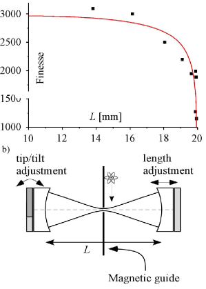
For miniaturization of optical components for atomic physics several proposals on atom chip integration have been presented Hor03 ; Lev04 ; Ros04 ; Mok04 ; Arm03 ; Liu05 . In our approach optical fibers are attached to the chip to form fiber-based cavities and to make small dipole traps. For fiber cavity experiments it is interesting to put atoms into the optical resonator. To place the atom inside the cavity it is possible to cut the fiber into two pieces and place the atom in the fiber gap. It is also possible to use a hollow fiber and guide the atom inside it Key00 . Because it is quite difficult to load atoms into a hollow fiber, especially if it is mounted on a micro-structured surface, the following section deals with fiber-gap-fiber configurations as the ones outlined in Fig. 1.
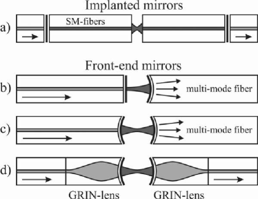
One realization of a fiber cavity is to implant mirrors into the fibers, such as Bragg gratings or dielectric coatings inserted between fiber pieces. See Fig. 1a). This has the advantage that the interaction volume (the gap where the atoms pass) is defined only by the bare fiber tips. Thus only the fiber itself has to be mounted on the atom chip with little or no need for alignment actuators. Mirrors and tuning actuators can be placed far from the gap. This allows a higher integration of the optics. A disadvantage of this method is that the cavity becomes quite long and that the extra interfaces increase the optical loss of the cavity. Using a long cavity will increase the mode volume and therefore also reduce . For atom detection the length of the cavity is fortunately not a very important parameter, as indicated by Eq. (9).
III.1 Loss mechanisms for a cavity
The quality of an optical resonator is described by its finesse. The finesse is related to the losses by:
| (14) |
where are the loss probabilities for the different loss channels. For example, a cavity mirror transmittance of corresponds to . As long as the cavity finesse is accurately calculated by Eq. (14). For further details on resonators we again refer to Sie86 . For atom detection it is desirable to obtain a high signal-to-noise ratio. This does not automatically mean that the finesse should be maximized. The signal-to-noise ratio for atom detection in the weak coupling and low atomic saturation is given by Eq. (9), where describes the mirror transmittance and is the total cavity loss. This implies that which is maximized for . For each kind of cavity there is an optimal choice for the mirror transmittance.
When the cavity contains a gap (See Fig. 1a) the main loss mechanism is related to the reduced coupling efficiency across the gap. This loss depends mainly on three things. (1) It is clear that the mode matching of the two fibers is not optimal and losses will occur as the gap is traversed. This loss increases with the gap size. (2) Also, in the case of transverse misalignment of the two fibers modes are not well-matched at the fiber facets. (3) A tilt between the two fibers also increases the mismatch between the two modes. In this case the loss also increases with the length of the fiber gap.
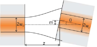
Figure 2 sketches these misalignments of the gap. The power coupling efficiency for two fibers can be calculated in the paraxial approximation by the overlap integral of the involved transverse mode functions.
| (15) |
where are the fiber optical field modes, and is the plane coinciding with one of the fiber facets. In this text we use this measure to describe cavity losses.
III.2 Losses due to the gap length
It is obvious that the losses increase with expanding gap size . The light exiting the first fiber at diverges until it hits the opposite fiber at a distance . We can describe the light leaving the first fiber as
| (16) |
where is the Gaussian waist at the first fiber facet, the radius of curvature, the beam radius, the Rayleigh length, and the Gouy-phase. The wavelength is and the wavenumber in the medium between the fibers with refractive index . The wavelength and the wavenumber in vacuum are and , respectively. Assuming that the two fibers are identical, the mode function at the facet of the second fiber is
| (17) |
The loss due to the length of the gap can be calculated from the overlap between functions (16) and (17).
| (18) | |||||
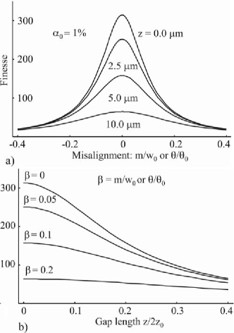
Here the transverse and angular misalignments are assumed to be zero. A plot of a finesse measurement with varying gap size is shown in Fig. 9a. In this case mirrors with a loss of 1% are assumed to be located inside the fibers. This loss is decreased if the gap between the fibers is small and the fiber has a small numerical aperture i.e. a large . However, to detect atoms should be small, as indicated by Eq. (9).
III.3 Losses due to transversal misalignment
If the two fibers are transversally misaligned to each other there will also be a mode mismatch when the light is coupled between the fibers. This loss can easily be calculated from Eq. (15). Using normalized Gaussian mode functions for two identical fibers (with ) with waist choosing the gap and angular misalignment to be zero one has
| (19) | |||||
where is the transverse misalignment of one of the fibers. This gives a loss due to the transversal misalignment :
| (20) | |||||
where the last approximation is valid only for . A plot of a finesse measurement with varying transversal misalignment is shown in Fig. 9b.
III.4 Losses due to angular misalignment
Another kind of loss emerges from angular misalignment of the two optical axes of the fibers. This is calculated by performing a basis change of Eq. (16) and evaluating the overlap given by Eq. (15). The mode leaving the first fiber (see Fig. 2) is approximately described by
| (21) |
for small neglecting diffraction effects. For a small rotation around the y-axis is given by
| (31) | |||||
| (38) |
Transforming into the coordinate system the mode function for the incident beam at the input plane of the second fiber becomes
| (39) |
The mode function for the second fiber at the input plane is given by
| (40) |
The loss due to a pure angle misalignment can be calculated from the overlap between functions (39) and (40).
| (41) | |||||
with . In general these misalignments are not independent of each other. The combined formula for all the misalignment losses is given by Sar79 :
| (42) |
with . A setup with transversal and longitudinal displacement and angle misalignment is plotted in Fig. 9. One experimental advantage is that the loss rate depends quadratically on small misalignments.
III.5 Fresnel reflections
Another effect that has to be taken into account is the reflection of light at the interfaces between the fibers and the introduced gap. It results from the step in the refractive index and is called Fresnel reflection. For a typical fiber in air or vacuum a fraction of of the incident light is reflected from a polished flat connector. In the case of a fiber gap cavity, these additional reflections lead to a system of three coupled resonators. While for any system of coupled resonators stationary solutions exist, i.e. eigenmodes of the electromagnetic field, they will in general not be equidistantly distributed in the frequency domain.
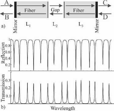
In a simple one-dimensional model, the coupled cavity system can be treated as a chain of transfer matrices Sie86 . Figure 4 shows the calculated reflected and transmitted intensities for a model resonator of rather low finesse.
The light intensity inside the gap depends on the specifics of the mode. This changes the overall losses, as can be seen in Fig. 4b. Consequently the reflected and transmitted intensities vary from mode to mode. The effect is strongest when the gap length is a multiple of . In experiments coupling atoms to the light field it has to be considered that the intensity inside the gap depends on the order of the mode and on the exact length of the gap. In absorption experiments only the relative change of transmitted light intensity is measured, which remains mode independent for light intensities well below saturation. Never the less it leads to a mode dependent signal-to noise ratio. Using fibers with =1.5 and intensities below atomic saturation the SNR changes by roughly 15%
IV Other fiber optical components for the atom chip
Not only cavities can be mounted on the surface of an atom chip. Miniaturization offers various advantages for a couple of other optical components. Lenses with extremely short focal lengths can be used to focus light to small areas. Such devices can be used to generate very tight dipole traps Sch01 ; Sch02 ; Rey03 , or to collect light from very well-defined volumes Eri05 .
IV.1 Fluorescence and absorption detectors
A fluorescence detector can be built using a single mode tapered lensed fiber and a multi-mode fiber. In this case, the tapered fiber is used to optically pump the atom. The multi mode fiber is used to collect the fluorescent light. For this configuration one can put the multi mode fiber at any angle with respect to the tapered lensed fiber. At small angles, atoms located in the focus of the tapered lensed fiber will scatter light away from the multi mode fiber. This would constitute an absorption detector. Such a device is illustrated in Fig. 7c). If the angle between the two fibers is sufficiently large only the fluorescent emission from the atom will be collected by the multi mode fiber. A picture of a fluorescence detector setup is shown in Fig. 7b). If no atom is present in the beam focus, very little light is scattered into the fiber. As soon as an atom is present, this signal increases. For single atom detection these two techniques are not sensitive enough, because photon recoils will expel the atom from the detection region and the multi mode fiber only collects a few photons. Therefore one must also trap the atom(s) in the tapered lensed fiber focus. This can be accomplished by a dipole trap.
IV.2 A single mode tapered lensed fiber dipole trap
To increase the number of detectable photons, the atom can be trapped inside the area where it interacts with the light. One possibility is to hold the atom in place with a dipole trap. An atom with transition frequency is attracted to the intensity maximum of a red-detuned laser beam (). A focussed laser beam forms an atom trap in the beam focus. For a far-detuned dipole trap quantities such as trap depth, lifetime and number of scattered photons can be estimated easily. A detailed derivation of dipole trap parameters discussed in the following paragraph can be found in Gri00 . The potential depth of a dipole trap is
| (43) |
and the scattering rate is given by
| (44) |
where and are the detunings of the laser with respect to the D2 and D1 lines of the alkali atom. The formulas apply to alkali atoms with a laser detuning much larger than the hyperfine structure splitting and a scattering rate far from saturation. It follows that the scattering rate for a given potential can be decreased by choosing a larger detuning and a higher laser intensity. The potential depth scales as , whereas the scattering rate scales as .
The D2 line of Rubidium, , has a wavelength of 780 nm, and the D1 line has a wavelength of 795 nm. A standard tapered lensed fiber generates a typical waist of µm at a wavelength of 780 nm. Far off resonance dipole traps can be realized with easy to use, high power diode lasers at a wavelength of 808 nm. Standard single mode lasers diodes are available with a power up to 150 mW. Assuming a coupling efficiency into the fiber of around 20%, one gets 30 mW of laser power in the dipole trap. These parameters yield a trap depth of 3.9 mK, and a transverse (longitudinal) trap frequency of 80 kHz (6 kHz). The heating rate for the dipole light is almost negligible. Experiments have shown that the lifetime is mainly limited by the background pressure of the vacuum chamber Mil93 .
Using resonant light to detect an atom increases the number of scattered photons as well as the heating rate enormously. In this case the trap lifetime drops to below a millisecond, which yields several thousands scattered photons before the atom is lost.
A multi mode fiber as detector at a distance of 40 µm can collect 2% of the fluorescent emission (See Fig. 7b). Assuming a detector efficiency of 60% (APD-based photon counter), including additional losses in the rest of the optical detector setup, it should be possible to detect about 100 photons during the trap lifetime. The signal-to-noise ratio is difficult to calculate without knowing the background noise.
V Integration of fibers on the atom chip
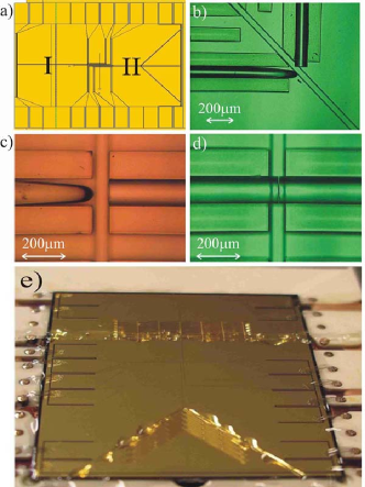
A method for mounting fibers accurately is needed to integrate the above devices with atom chips. Fibers can be held at the right place with the help of some kind of fiber grippers, aligned and finally glued to the chip. This strategy will not work well for fiber cavities because they need to be actively aligned during operation (See Fig. 1b-d). For active alignment of an on-chip cavity an actuator is needed. Useful actuators, such as piezoelectric stacks, are quite large compared to the fibers. Typical dimensions exceed 2x2x2mm. This places restrictions on the level of optical integration one can obtain on the chip. Components that don’t need active alignment, such as the cavities with implanted mirrors (See Fig. 1a) or tapered fibers for dipole traps, can be directly integrated on the chip. To obtain a high degree of precision in the mounting we have developed a lithographic method where a thick photoresist is patterned to form the mounting structures Liu05 .
V.1 Building fiber cavities
We have so far realized cavities with curved and planar mirrors at the front-end of two fibers, and cavities with implanted mirrors made out of one piece of fiber with a gap for the atoms similar to the ones shown in Fig. 1.
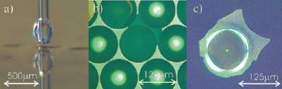
The mirror coatings are attached to the fibers using a transfer technique. In this process, dielectric mirror coatings with a transmittance of 0.1% to 1% are manufactured on a glass substrate. The substrate is either flat or contains an array of spherical microlenses for curved coatings. The adhesion between the coating and the glass substrate is fairly low. When the coating is glued to an optical fiber it is possible to transfer the coating from the substrate to the fiber Jena . A series of pictures showing this transfer is found in Fig. 5.
The transmittance T is chosen to be around 1% for cavities with implanted mirrors (Fig. 1a) because of the higher loss. For the front-end mirrors (Fig. 1b-d), the loss is lower therefore it is more suitable to choose a mirror with transmittance around 0.1% to obtain a high SNR for the detection of atoms.
The higher loss for cavities with implanted mirrors has several origins in addition to the ones caused by the gap. For some of our cavities the main intrinsic loss sources are the glue layers holding the mirror coatings to the fibers. These glue layers are typically a few micrometers thick. The transversal confinement of the fiber is absent in the glue layers as well as in the mirror coatings. This leads to losses similar to the ones discussed for the gap length, i.e Eq. (18). Glued mirrors are also sensitive to angular misalignment, which can be treated by Eq. (41).
Curved coatings may be used to build a concave cavity with front-end mirrors. With this design we reached a finesse of greater than 1000 as shown in Fig. 6. Complications due to Fresnel reflections do not exist for the front-end cavity. The quality of the mirrors and their alignment determine how high the finesse may become. The mode profile of the optical fiber does usually not match the cavity mode. This leads to a poor incoupling into the front-end cavity. This problem can be solved by transferring the mirror coatings to a tapered fiber, or a small grin lens to focus the light into the cavity mode. This unfortunately leads to a more complicated and error prone fabrication process. In addition, a cavity with front-end mirrors must be mounted on alignment actuators for efficient tuning of the cavity. This makes miniaturization and integration of multiple cavities harder.
A cavity with the geometry shown in Fig. 1a) was built by inserting two planar mirrors into a fiber with length about 10 cm. This fiber cavity is subsequently cut into two halves and the new surfaces are polished. This cavity has the advantage that it is very easy to align and mount. An actual cavity of this kind is shown in Fig. 7d) where the cavity is mounted on an atom chip using a SU-8 structure to hold the fibers. The drawback with this cavity geometry is that the finesse is rather low compared to the front-end mirrors, mainly because of the fiber gap and the glue layers as described above. Cavities with inserted mirrors typically reach a finesse of a few hundred instead of a few thousand as for the front-end cavities. The losses due to the glue layers could be reduced by direct coating of the fiber instead of using the transfer technique. The losses due to the gap itself could also be reduced by introducing collimation optics in the gap, such as a small grin lens or a tapered fiber. Such additional optics will however introduce additional Fresnel reflections and may also require active alignment of the gap, as for the front-end cavity.
V.2 The SU-8 resist
To mount fibers on the atom chip a lithographically patterned photoresist called SU-8 was used. SU-8 is an epoxy based negative resist with high mechanical, chemical and thermal stability. Its specific properties facilitate the production of thick structures with very smooth, nearly vertical sidewalls Liu05 . It has been used to fabricate various micro-components. Examples include optical planar waveguides with high thermal stability and controllable optical properties. Mechanical parts such as microgears Sei02 for engineering applications, and microfluidic systems for chemistry Duf98 have also been built. The SU-8 is typically patterned with 365-436 nm UV-light.
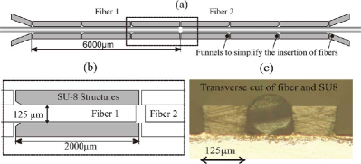
To assess the quality of the alignment structures, we use the SU-8 structures to hold fiber optical resonators. The finesse of the resonator strongly depends on losses introduced by misalignment as described by Eq. (42). The layout of the used alignment structure with fibers is shown in Fig. 8. This design includes funnels to simplify assembly. To avoid angular misalignment the total length of the alignment structure is quite long (6000 µm). The structure is divided into several subsegments to reduce stress induced by thermal expansion.
V.3 Test of the SU-8 structure
The quality of the SU-8 fiber splice was determined by measuring the finesse of a mounted resonator. The finesses of two intact fiber resonators were found to be and . After cutting the fiber and polishing the new surfaces, the two fiber pieces were introduced into the SU-8 structures. We observed the fiber ends under a microscope and minimized the gap size. For these resonators the finesses were found to be and . This corresponds to an additional average loss of )%. Neglecting other additional losses, this corresponds to a transversal misalignment of nm or an angular misalignment of rad . To test thermal stability the temperature of the substrate was varied between 20 ℃ and 70 ℃. The finesse of the inserted fiber resonator showed no change during heating.
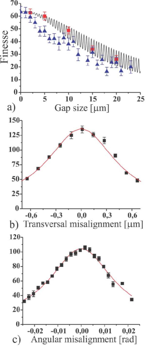
Another test for the quality of the SU-8 structures was a finesse measurement as a function of gap size. One measurement was done in the SU-8 structures and one outside the structures. The measurement outside was performed with nanopositioning stages, which in principle can be tuned to a few nanometers. With the positioning stages the finesse was optimized. Nevertheless, the finesse obtained inside the SU-8 structures always remained higher than the ones obtained using the positioning stages. The results of these measurements are shown in Fig. 9a). The structures have also allowed long-term stability of the cavities in a high-vacuum environment.
VI Pilot test for atom detection with small waists
To assess the consequences of Eq. (9) a test using a macroscopic cavity was performed Haa05b . The goal was to detect atoms with a cavity with moderate finesse and a very small mode diameter.
VI.1 Dropping atoms through a concentric cavity
To explore atom detection using cavities with small waists, we built a magneto-optical trap (MOT) for 85Rb atoms approximately 20 mm above the center of a near concentric cavity with a finesse of about 1100 formed by normal high-reflectance mirrors. The MOT contained atoms at a temperature of 35 µK. In a first experiment, we switched off the trap completely and monitored the atomic cloud as it fell freely through the cavity. This configuration was used to estimate the detection sensitivity of the cavity.
We measured the light intensity transmitted through the cavity with an amplified photodiode for high light intensities or with a photomultiplier tube (PMT) for low light intensities. The PMT provided a near shot-noise limited detection. The low-noise electronic amplification limited the detection bandwidth to 20 kHz. The main source of technical noise in our setup was due to mechanical vibrations of the vacuum chamber that held the cavity.
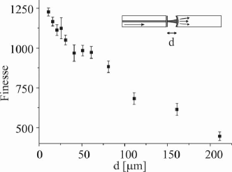
To minimize the influence of vibrations and long term drifts one of the cavity mirrors was mounted on a piezoelectric tripod that allowed us to keep the TEM00 mode centered on the cavity axis. The second mirror was mounted on a translating piezoelectric stage for wavelength stabilization. Figure 10 illustrates how the cavity finesse was reduced as the concentric point was approached for our cavity formed by two mirrors with a radius of curvature of mm and a transmittance . For a mirror separation far less than the concentric limit the cavity had a finesse of 3000. The finesse dropped to 1100 when the separation was 70 µm from the concentric point. The cavity mode waist was 12.1 µm for this separation.
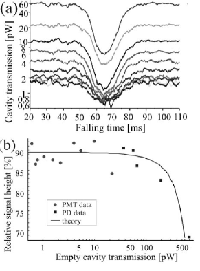
The drop in the cavity transmission signal from freely falling atoms is plotted in Fig. 11a). The different curves show different pump powers, corresponding to empty cavity transmissions between 1 pW and 600 pW. The atom number in the MOT is , the signal drops by 90 as long as the atomic transition is not saturated (Fig. 11b). Combining the results of Hor03 with Eq. 11 the effective atom number becomes . This was consistent with an independent atom number measurement based on fluorescence imaging. To determine the sensitivity limit of the cavity detector, the number of atoms in the MOT was gradually reduced until the MOT contained atoms. This atom number produced a signal drop of approximately . We consider this to be the sensitivity limit. A theoretical fit results in an effective atom number sensitivity of .
VI.2 Detecting Magnetically Guided Atoms
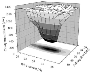
As a next step, atoms were magnetically guided to the cavity center using a wire guide Den99 . By changing the current in the guiding wire the overlap between the atoms and the cavity mode could be adjusted. In Fig. 12 we plot the cavity transmission as the position of the magnetic guide is varied across the cavity mode. As the atomic overlap with the cavity mode was increased, we observed an increased drop in cavity transmission. From the duration of the drop in transmission the temperature of the guided atoms could be determined to be 25 µK.
The density distribution for the atoms was much larger than the Rayleigh volume of the cavity. Consequently, it was not possible to distinguish individual atoms in the guide using our cavity. This cavity would show a detectable change in the transmission signal if a single atom crossed the region of maximum coupling as can be as small as . The precision in the positioning can be improved using magnetic microtraps produced by atom chip surface traps Fol02 . To achieve the same detection sensitivity with a cavity mode diameter of 2 µm a finesse of 40 would be sufficient.
VII Conclusion
In this article we have explored and compared various methods of detecting single atoms on an atom chip. Miniaturization brings advantages for such detectors. To detect atoms with a cavity, the requirements on the cavity finesse relaxes quadratically as the mode diameter of the cavity is decreased. This favorable scaling law was tested in a pilot experiment where atoms were detected when magnetically guided through a near-concentric cavity
The simplest way to get to a fully integrated atom detector on an atom chip is to mount optical fibers on to the surface of the chip. Such fiber devices can be used for fluorescence, absorption, and cavity assisted detection of single atoms. To integrate fibers, we have developed a precise lithographic method that allows robust positioning of fibers to within ¡150 nanometers. The high accuracy allows very reliable fiber-to-fiber coupling, suitable for integration of fiber cavities (Fig. 1a). We have built and integrated a fiber cavity on an atom chip which should be able to detect a single atom with a SNR of better the 5 within a measurement time of 10 µs. The same lithographic method has been used to position tapered lensed fibers on the chip. These can be used to combine dipole traps and fluorescence/absorption detectors.
We acknowledge financial support from the Landesstiftung Baden-Württemberg, Forschungsprogramm Quanteninformationsverarbeitung and the European Union, contract numbers IST-2001-38863 (ACQP), MRTN-CT-2003-505032 (Atom Chips), and HPRI-CT-1999-00114 (LSF). The atom chip shown in this work was fabricated at the The Braun Submicron Center at Weizmann Institute of Science.
References
- (1) R. Folman, P. Krüger, J. Schmiedmayer, J. Denschlag, and C. Henkel. Microscopic atom optics. Adv. At. Mol. Phys., 48:263, 2002.
- (2) C. Henkel, J. Schmiedmayer, and C. Westbrook, editors. Special Issue: Atom chips, volume 35. Eur. Phys. J. D, 2005.
- (3) R. Folman, P. Krüger, D. Cassettari, B. Hessmo, T. Maier, and J. Schmiedmayer. Controlling cold atoms using nanofabricated surfaces: Atom chips. Phys. Rev. Lett., 84:4749, 2000.
- (4) P. Krüger, X. Luo, M.W. Klein, K. Brugger, A. Haase, S. Wildermuth, S. Groth, I. Bar-Joseph, R. Folman, and J. Schmiedmayer. Trapping and manipulating neutral atoms with electrostatic fields. Phys. Rev. Lett., 91:233201, 2003.
- (5) W. Hänsel, J. Reichel, P. Hommelhoff, and T. W. Hänsch. Magnetic conveyor belt for transporting and merging trapped atom clouds. Phys. Rev. Lett., 86:608, 2001.
- (6) D. Cassettari, B. Hessmo, R. Folman, T. Maier, and J. Schmiedmayer. Beam splitter for guided atoms. Phys. Rev. Lett., 85:5483, 2000.
- (7) D. Müller, E. A. Cornell, M. Prevedelli, P. D. D. Schwindt, and A. Zozulyaand D. Z. Anderson. Waveguide atom beam splitter for laser-cooled neutral atoms. Opt. Lett., 25:1382, 2000.
- (8) T. Schumm, S. Hofferberth, L. M. Andersson, S. Wildermuth, S. Groth, I. Bar-Joseph, J. Schmiedmayer, and P. Krüger. Matter-wave interferometry in a double well on an atom chip. Nature Physics, 1:57, 2005.
- (9) P. Hommelhoff, W. Hänsel, T. Steinmetz, T. W. Hänsch, and J. Reichel. Transporting, splitting and merging of atomic ensembles in a chip trap. New J. Phys., 7:3, 2005.
- (10) H. Ott, J. Fortagh, G. Schlotterbeck, A. Grossmann, and C. Zimmermann. Bose-Einstein condensation in a surface microtrap. Phys. Rev. Lett., 87:230401, 2001.
- (11) W. Hänsel, P. Hommelhoff, T.W. Hänsch, and J. Reichel. Bose-Einstein condensation on a microelectronic chip. Nature, 413:498, 2001.
- (12) S. Schneider, A. Kasper, Ch. vom Hagen, M. Bartenstein, B. Engeser, T. Schumm, I. Bar-Joseph, R. Folman, L. Feenstra, and J. Schmiedmayer. Bose-Einstein condensation in a simple microtrap. Phys. Rev. A, 89:023612, 2003.
- (13) P. W. H. Pinkse, T. Fischer, P. Maunz, and G. Rempe. Trapping an atom with single photons. Nature, 404:365, 2000.
- (14) P. Horak, B. G. Klappauf, A. Haase, R. Folman, J. Schmiedmayer, P. Domokos, and E. A. Hinds. Possibillity of single-atom detection on a chip. Phys. Rev., A67:043806, 2003.
- (15) R. Long, T. Steinmetz, P. Hommelhoff, W. Hänsel, T. W. Hänsch, and J. Reichel. Magnetic microchip traps and single atom detection. Phil. Trans. R. Soc. Lond., 361:1375, 2003.
- (16) B. Lev, K. Srinivasan, P. Barclay, O. Painter, and H. Mabuchi. Feasibility of detecting single atoms using photonic bandgap cavities. Nanotechnology, 15, S556-S561 (2004).
- (17) M. Rosenblit, P. Horak, S. Helsby, and R. Folman. Single-atom detection using whispering-gallery modes of microdisk resonators. Phys. Rev., A70:053808, 2004.
- (18) S. Eriksson, M. Trupke, H. F. Powell, D. Sahagun, C. D. J. Sinclair, E. A. Curtis, B. E. Sauer, E. A. Hinds, Z. Moktadir, C. O. Gollasch, and M. Kraft. Integrated optical components on atom chips. Eur. Phys. J D, 35:135, 2005.
- (19) D. Leibfried, M. D. Barrett, T. Schaetz, J. Britton, J. Chiaverini, W. M. Itano, J. D. Jost, C. Langer, and D. J. Wineland. Toward Heisenberg-limited spectroscopy with multiparticle entangled states. Science, 304:1476, 2004.
- (20) Y. Miroshnyenko, D. Schrader, S. Kuhr, W. Alt, I. Dotsenko, M. Khudaverdyan, A. Rauschenbeutel, and D. Meschede. Continued imaging of the of a single neutral atom. Opt. Express, 11:3498, 2003.
- (21) S. J. van Enk and H. J. Kimble. Single atom in free space as a quantum aperture. Phys. Rev. A, 61:051802, 2000.
- (22) S. J. van Enk and H. J. Kimble. Strongly focused light beams interacting with single atoms in free space. Phys. Rev. A, 63:023809, 2001.
- (23) S. J. van Enk. Atoms, dipole waves, and strongly focused light beams. Phys. Rev. A, 69:043813, 2004.
- (24) S. Kadlecek, J. Sebby, R. Newell, and T. G. Walker. Nondestructive spatial heterodyne imaging of cold atoms. Opt. Lett., 26:137, 2001.
- (25) M. R. Andrews, M. O. Mewes, N. J. van Druten, D. S. Durfee, D. M. Kurn, and W. Ketterle. Direct, nondestructive observation of a Bose condensate. Science, 273:84, 1996.
- (26) L. D. Turner, K. P. Weber, D. Paganin, and R. E. Scholten. Off-resonant defocus-contrast imaging of cold atoms. Opt. Lett., 29:232, 2004.
- (27) J. J. Hope and J. D. Close. Limit to minimally destructive optical detection of atoms. Phys. Rev. Lett., 93:80402, 2004.
- (28) J. E. Lye, J. J. Hope, and J. D. Close. Rapid real-time detection of cold atoms with minimal destruction. Phys. Rev., A69:023601, 2004.
- (29) J. J. Hope and J. D. Close. General limit to nondestructive optical detection of atoms. Phys. Rev., A71:043822, 2004.
- (30) P. R. Berman. Cavity Quantum Electrodynamics. Academic press, San Diego, 1994.
- (31) A. E. Siegman. Lasers. University Science Books, Mill Valley, 1986.
- (32) Z. Moktadir, E. Koukharenka, M. Kraft, D. M. Bagnall, H. Powell, M. Jones, and E. A. Hinds. Etching techniques for realizing optical micro-cavity atom traps on silicon. J. Micromech. Microeng., 14:82, 2004.
- (33) D. Armani, T. Kippenberg, S. Spillane, and K. Vahala. Ultra-high-Q toroid microcavity on a chip. Nature, 421:925, 2003.
- (34) X. Liu, K. H. Brenner, M. Wilzbach, M. Schwarz, T. Fernholz, and J. Schmiedmayer. Fabrication of alignment structures for a fiber resonator by use of deep-ultraviolet lithography. Applied Optics, 44, 6857 (2005).
- (35) M. Key, I. G. Hughes, W. Rooijakkers, B. E. Sauer, E. A. Hinds, D. J. Richardson, and P. G. Kazansky. Propagation of cold atoms along a miniature magnetic guide. Phys. Rev. Lett., 84:1371, 2000.
- (36) M. Saruwatari and K. Nawate. Semiconductor laser to single-mode fiber coupler. Appl. Opt., 18:1847, 1979.
- (37) N. Schlosser, G. Reymond, I. Protsenko, and P. Grangier. Sub-poissonian loading of single atoms in a microscopic dipole trap. Nature, 411:1024, 2001.
- (38) N. Schlosser, G. Reymond, and P. Grangier. Collisional blockade in microscopic optical dipole traps. Phys. Rev. Lett., 89:023005, 2002.
- (39) G. Reymond, N. Schlosser, I. Protsenko, and P. Grangier. Single-atom manipulations in a microscopic dipole trap. Phil. Trans. R. Soc. Lond. A, 361:1527, 2003.
- (40) R. Grimm, M. Weidemüller, and Y. Ovchinnikov. Optical dipole traps for neutral atoms. Advances in Atomic, Molecular and Optical Physics, 42:95, 2000.
- (41) J. D. Miller, R. A. Cline, and D. J. Heinzen. Far-off-resonance optical trapping of atoms. Phys. Rev., A47:4567, 1993.
- (42) Optische Interferenz Bauelemente GmbH. For further details: http://www.oib-jena.de.
- (43) V. Seidemann, J. Rabe, M. Feldmann, and S. Büttgenbach. SU8-micromechanical structures with in situ fabricated movable parts. Microsyst. Tech., 8:348, 2002.
- (44) D. Duffy, O. Schueller J. McDonald, and G. Whitesides. Rapid prototyping of microfluidic systems in poly(dimethylsiloxane). Anal. Chem., 70:4974, 1998.
- (45) A. Haase, B. Hessmo, and J. Schmiedmayer. Detecting magnetically guided atoms with and optical cavity. Opt. Lett. 31, 268-270 (2006).
- (46) J. Denschlag, D. Cassettari, and J. Schmiedmayer. Guiding neutral atoms with a wire. Phys. Rev. Lett., 82:2014, 1999.