Key Laboratory for Quantum Optics, Shanghai Institute of Optics and Fine Mechanics, Chinese Academy of Sciences, Shanghai, China, 201800
opticalman@gmail.com
A Radio-Frequency Atom Chip for Guiding Neutral Atoms
Abstract
We propose two kinds of wire configurations fabricated on an atom chip surface for creating two-dimensional (2D) adiabatic rf guide with an inhomogeneous rf magnetic field and a homogenous dc magnetic field. The guiding state can be selected by changing the detuning between the frequency of rf magnetic field and the resonance frequency of two Zeeman sublevels. We also discuss the optimization of loading efficiency and the trap depth and how to decide proper construction when designing an rf atom chip.
020.7010, 020.1670, 230.3990
1 Introduction
Magnetic field is widespread used for manipulating neutral atoms and becomes a powerful tool for studying the physics of atoms [1]. Accurate metal wires at a scale of micron can be fabricated in a chip with lithographic or other standard surface-patterning process [2]. This kind of chip can realize miniaturized electric or magnetic traps and guides which can manipulate neutral atoms close to the chip surface [3, 4, 5, 6, 7, 8]. Compared to the common magnetic coil, the atom chip can not only create tightly atom traps with large field gradients and high field curvature without the need for large current and large volume, but versatile and tiny traps without complex structure and design. This permits the controlled tunneling of atoms over micron or sub-micron lengths and makes it a natural platform for applications in coherent matter-wave control such as miniaturized atom interferometer, quantum information process, and the study of low-dimensional quantum gases [9]. But ordinary atom chips use static magnetic field for atom trapping, only weak-field-seeking atoms (excited spin state atom) can be trapped since strong-field seeking atoms (ground spin state atoms) need the maxima of magnetic field and this kind of magnetic field is not allowed by Maxwell’s equations. For weak-field-seeking atoms, spin of excited spin states relax to the ground state at a density-dependent rate, afterwards these atoms are ejected from the trap [10]. This can be overcame by using ac magnetic field. R. Lovelace et al [11] proposed a dynamic magnetic trap using ac magnetic field for trapping which can trap strong-field seeking atoms. Then C. Agosta et al [12] proposed another scheme using microwave radiation which is realized experimentally by R. Spreeuw et al [13], but the equipment is complex and difficult to realize. In comparison with microwave, rf technique has been used widespread in forced evaporative cooling and other applications of neutral atoms and easily manipulated in experiment. Recently the rf magnetic field is introduced to realize rf adiabatic trap combining with a dc Ioffe-Pritchard trap[14, 15, 16]. In comparison to the optical trap, spontaneous radiation can be ignored in this kind of rf magnetic trap and the energy level is finite and can be calculated easily.
In this article we propose an rf atom chip for guiding atoms in strong-field seeking state. In Section 2 we discuss the theory of adiabatic rf guide and then two kinds of guide configurations are proposed. In Section 3 parameters of the guides and loading efficiency are also discussed. In Section 4 we discuss the problems and solutions concerning design of an rf atom chip.
2 Theory of Adiabatic Radio-Frequency Guide
Now the dressed state method is introduced for calculating the eigenstate and eigenenergy. We consider a neutral atom in ground state which has five zeeman sublevels () . Hamiltonian of an atom in rf magnetic field with a dc bias magnetic field is given by
| (1) |
where is the Hamiltonian of the rf field, is the atom-field coupling strength which is given in magnetic-dipole and rotating-wave approximation by with . is the atomic Hamiltonian which is given by
| (2) |
where is the magnetic dipole moment of the atom, is the resonance frequency with the Bohr magneton , The Landé factor and the homogeneous dc magnetic field along the Y-axis as shown in Fig. 1. And is the y component of which is given by atomic angular momentum . Supposing that atomic velocity is so small that atom motion cannot excite the transitions among the internal states, one can use Born-Oppenheimer approximation to separate the whole wave-function of the global system into two parts: one is the external state of atom motion and another is the internal state of atom in rf field. Afterwards, two separated but correlative equation is given by
| (3) | |||
| (4) |
where is dressed atom Hamiltonian with its eigenvalues of . All of five dressed eigenenergies of can be obtained as
| (5) |
where , and the detuning . It should be paid attention to that the result uses the rotating wave approximation. The proposal of O. Zobay et al [14] starts from a static Ioffe-Pritchard trap and then superimposes a homogeneous oscillatory rf field where is homogeneous and has inhomogeneous spatial distribution. Our proposal reverse the idea and starts from a homogenous magnetic field (bias field ) and superimposes an oscillatory rf field varying in the space. The results will go beyond the reversion and there will come some new phenomena. As shown in Equation (5), for the rf magnetic field with a minimum at its center (simplest configuration is a quadrupole rf magnetic field), only and have a minimum at minimum point of rf field, so their eigenstate become trapped state which is given by
| (6) | |||||
| (7) | |||||
where the angle
| (8) |
and is eigenstate of when atom-field coupling with ,, and the photon occupation number N. When , and and approach and respectively . Then the trapped state is predominated by the -like state. If we prepare atoms in Zeeman sublevel by optical pumping, atoms will project into trapped state mostly, the less part into and little residual into untrapped states after they couple with a quadrupole rf magnetic field. This differs from the static magnetic trap that can only trap the states with and or and . Actually is not always true which will make more atoms projecting into untrapped states and atom loss becomes notable. We will study this problem in Section 3. And it must be pointed out that only the rf field components being perpendicular to the dc bias magnetic field contribute to the trap which means only a 2D guide will be created and there is no trapping potential along the direction of [15].
3 Adiabatic Radio-Frequency Guide from Planar Wires
As shown above, in addition to a homogenous static magnetic field ( in Fig. 1), a 2D Radio-Frequency quadrupole field is needed for the rf guide which is usually created by a pair of anti-Helmholtz coils. But there will be a contradiction between the huge inductive reactance in radio-frequency range and the adequate current for sufficient trap depth and frequency. It is difficult to get impedance match between huge inductive reactance coils and a rf amplifier since the coils play a role of low-pass filter. Atom chip provides with a new solution for the dilemma which is made of planar wires fabricated in a microelectronic chip. Because atom chip consists of several metal wires on the surface of a chip, there will be little inductive and capacitive impedance for impedance matching easily, as well as a little resistance for small dissipation power. And the atom chip can provide huge gradient and curvature with relatively small current since they respectively scale as and ( is current and is characteristic size) [17]. Although the conclusion is made in direct current range, for the rf regime, if the distance from the chip ( is the wavelength of rf magnetic field), the problem will transform to a static field problem and the field amplitude can be calculated as a static magnetic field [21]. Now the frequency of the rf magnetic field is 10MHz and corresponding to a wavelength of 30m which meets the condition.
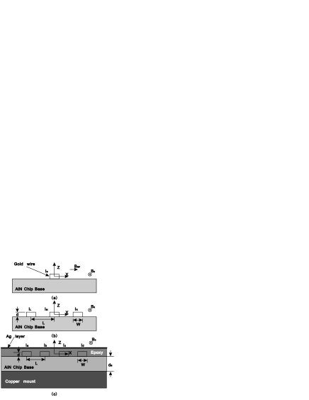
The simplest configuration for the 2D quadrupole field in an atom chip is a wire and a bias rf magnetic field perpendicular to the wire (Fig. 1a), which has been used for dc guided[7, 18, 19, 20]. There will be a zero-field point above the wire and a 2D quadrupole field around it in XZ-plane. The distance between the chip and the zero-field point depends on the ratio of the current and the strength of the bias field [17]. But the bias rf magnetic field is created by the outer coils which will encounter the same problem mentioned above. The solution is using wires in atom chip for creating the bias rf magnetic field instead of outer coils, as shown in Fig. 1b and c, both three-wire and four-wire configuration are able to create requisite 2D rf quadrupole field.
Firstly wires are considered as infinitely thin and long, which is a good approximation when characteristic distance from the chip surface is bigger than the wire width and great smaller than the wire length [17]. Rf current is carried by the wires where are shown in Fig. 1b and c and dc field is created by outer coils. According to equation (5), in the case of trapped state , the adiabatic rf potential of three-wire and four-wire configuration respectively,
| (9) |
and rf magnetic field and are given by
| (10) | |||||
| (11) | |||||
Fig. 2 shows adiabatic rf potential in XZ-plane.
Afterwards the guide centers of three-wire and four-wire configuration can be found at and respectively, where both and are in the minimum point. The guide centers are independent with current amplitude and detuning and merely decided by the geometry configuration. Around the guide centers, Taylor series of adiabatic rf potential is respectively given by ()
| (12) | |||||
| (13) | |||||
| (14) | |||||
| (15) |
is given by
| (16) |
According to the series, there appears constant and second terms and no linear item, thereby the adiabatic rf potential and approximates harmonic potential which is widespread available in static magnetic potential for cold atoms and BEC. The oscillation frequency along th coordinate axis of and is given by (m is atom mass)
| (17) |
It is apparent that the oscillation frequency of the three-wire and four-wire configuration has a fixed ratio of and each of them has the same oscillation frequency along and axis. We substitute the atom mass of Rubidium for and will derive a coefficient of (as shown in Equation (17)). The oscillation frequency is proportional to current amplitude and inversely proportion to square of and the root of . When becomes very small, the trap potential approach to a linear and the guide approaches to a 2D quadrupole guide and a huge oscillation frequency will be obtained. But the parameters can not be decided optionally and analysis as follows will disclosure the problem. After analysis of trap depth and transfer efficiency from Zeeman state to all of the trapped dressed states, a contradiction will be found which will make us select detuning carefully.
According to first derivative of Equation (9),we can find the maximum and minimum point of adiabatic rf potential and then trap depth is decided easily. It is interesting that the trap depth has the same form except a coefficient whether in three-wire and four-wire configuration or along X and Z axis. Afterwards the trap depth can be written in one equation which is given by
| (18) |
is the coefficient which is different in various situation and is given by
| (19) |
According to Equation (18), the trap depth is monotonely decreasing function of which is shown in Fig. 3. On the other hand, in order to reduce the loss due to the atoms overflowing from the guide, the trap depth should be larger than the mean atomic dynamic energy. This leads an empirical condition [17]
| (20) |
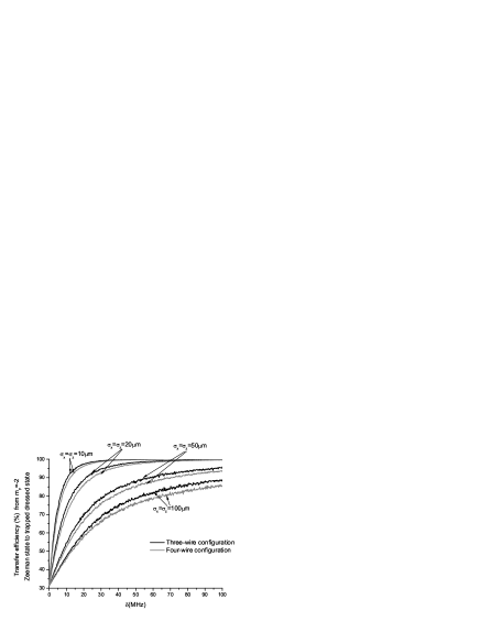
with in order to make this loss term negligible. In order to increase the trap depth, and should be reduced and should be increased. Once another situation is added, another limit will appear on selection of guide parameter which does not exist in common static magnetic trap. According to Section 2, the Zeeman state before the atoms are trapped is different from the adiabatic rf trapped state. When atoms are entering the guide, there will be a probability of transferring atoms from Zeeman state to adiabatic rf trapped state. According to Equation (6, 7, 8), The key parameter of transferring probability is , the bigger will increase the transferring probability. The denominator, Rabi frequency , is different in different spatial location because decided by amplitude of rf magnetic field which is a quadrupole form and not homogenous. On the other hand, the numerator is homogenous for a given guide. In both cases there will appear a spatial distribution of transferring probability. If atom cloud in Zeeman state is put in the guide center (after performed optical pumping very fast) and then adiabatic rf potential appears, the atoms near the guide center will derive a high transferring probability and the farther the atoms is from the guide center, the smaller transferring probability is. As shown in Fig. 4, the transferring probability of four-wire configuration is a little smaller than that of three-wire configuration, and the smaller atom cloud will derive the higher transferring probability. Also the bigger detuning will cause the higher transferring probability. But according to Fig. 3 the bigger detuning will cause the smaller trap depth, there is a contradiction when we select the parameter . We can not get the deeper trap depth by increasing current amplitude or reducing spacing between wires which will increase the Rabi frequency and reduce the transferring probability, so the simple idea for keeping trap depth and increasing transferring probability is reducing the size of atom cloud which can be realized by being compressed in a static magnetic trap or an optical dipole trap and then pumping to Zeeman state. For example, if the size of the atom cloud and we want to obtain eighty percent transferring probability, the detuning should be greater than and the trap depth is (four-wire) and (three-wire) along Z axis (the trap depth along X axis is much bigger than it along Z axis). According to Equation (20), the temperature of atom cloud should be smaller than and coincide with guide center precisely.
4 Design An Atom Chip with Adiabatic Radio-Frequency Guide
In common atom chip, almost all of parts is made from nonferromagnetic material and can be considered as transparent ones for magnetic field since they nearly do not change distribution of dc magnetic field. In contrast to it, the metal accessories around the rf atom chip must be considered because metal will change distribution of rf electromagnetic field since metal is a kind of good conductor. In order to create proper distribution of rf magnetic field, we should design the chip configuration carefully. Our atom chip is made by the technique developed by J. Reichel et al [3], as shown in Fig. 1(c), the fist layer is made from silver and about in thickness; the second layer is a kind of epoxy (Epotek 920)for fixing the silver layer and keeping gold wires on the chip away from the silver layer. Afterwards gold wires fabricated on an aluminium nitride chip base. Below the base, there is an oxygen-free copper mount for fixing the chip and elimination of heat. The epoxy and base is insulator and not ferromagnetic material, so they nearly do not effect the distribution of rf magnetic field. Whereas the silver layer and the copper mount are both metal material, their effect on rf magnetic field should be considered. In common chips, wire width , wire spacing , wire thickness and parameters about rf magnetic field, current amplitude , detuning and corresponding to which wavelength and skin depth is about for copper and silver. The silver layer of 200nm in thickness is almost transparent for the electromagnetic wave that we used although silver has very good conductivity. On the other hand, size of the copper mount is much bigger than the skin depth. After put onto a copper mount, rf magnetic field created by the chip will change. It is nearly impossible to calculate the distribution of the rf magnetic field by analytic solution. FEM (Finite Element Method) is used for obtaining numeric solution. As shown in Fig. 5, position of guide center goes far away from the chip surface when spacing between copper mount and chip decreases. Afterwards the adiabatic rf potential approaches the ideal configuration (without width and copper mount) when and some results are shown in Fig. 5 which show the effect of mount. But this approximation is only true near the guide center and great error will appear away from the guide center.
5 Conclusion
We have shown our rf atom chip to be applicable to realize a guide for atoms in strong-field seeking state. This technique may offer a new way for manipulating atoms on an atom chip and potential application in realizing atom interferometer and other fields in integrated atom optics. The 2D character may be used to realize coherent atom laser. If combined with surface induced evaporative cooling technique [22], an atom laser with continuous output may be realized.
We acknowledge financial support from the State Key Basic Research Program under Grant No. 2006CB921202, the National Natural Science Foundation of China under Grant No. 10334050, 10474105 and Key Oriental Project of Chinese Academy of Sciences under Grant No. KGCX2-SW-100.
References
- [1] C.E. Wieman, D.E. Pritchard, and D.J. Wineland, “Atom cooling, trapping, and quantum manipulation”, Rev. Mod. Phys. 71, S253 (1999).
- [2] M. Drndić, K. S. Johnson, J. H. Thywissen, M. Prentiss, and R. M. Westervelt, “Micro-electromagnets for atom manipulation”, Appl. Phys. Lett. 72, 2906 (1998).
- [3] J. Reichel, W. Hänsel, P. Hommelhoff, and T.W. Hänsch, “Applications of integrated magnetic microtraps”, Appl. Phys. B. 72, 81 (2001).
- [4] H. Ott, J. Fortagh, G. Schlotter, and C. Zimmermann, “Bose-Einstein condensation in a surface microtrap”, Phys. Rev. Lett. 87, 230401 (2001).
- [5] R. Folman, P. Krüger, D. Cassettari, B. Hessmo, T. Maier, and J. Schmiedmayer, “Controlling cold atoms using nanofabricated surfaces: Atom chips”, Phys. Rev. Lett. 84, 4749 (2000).
- [6] D. Müller, D. Z. Anderson, R. J. Grow, P. D. D. Schwindt, and E. A. Cornell, “Guiding neutral atoms around curves with lithographically patterned current-carrying wires”, Phys. Rev. Lett. 83, 5194 (1999).
- [7] N. H. Dekker, C. S. Lee, V. Lorent, J. H. Thywissen, S. P. Smith, M. Drndi, R. M. Westervelt, and M. Prentiss, “Guiding neutral atoms on a chip”, Phys. Rev. Lett. 84, 1124 (2000).
- [8] S. Du, M. B. Squires, Y. Imai, L. Czaia, R. A. Saravanan, V. Bright, J. Reichel, T. W. Hänsch, and D. Z. Anderson, “Atom-chip Bose-Einstein condensation in a portable vacuum cell”, Phys. Rev. A. 70, 053606 (2004).
- [9] J. Fortagh, H. Ott, A. Grossmann, C. Zimmermann, “Miniaturized magnetic guide for neutral atoms”, Appl. Phys. B. 70, 701 (2000).
- [10] A. Lagendijk, I. F. Silvera and B. J. Verhaar, “Spin exchange and dipolar relaxation rates in atomic hydrogen: Lifetimes in magnetic traps”, Phys. Rev. B. 33, 626 (1986).
- [11] R. V. E. Lovelace, C. Mehanian, T. J. Tommila an d D. M. Lee, “Magnetic confinement of a neutral gas”, Nature. 318, 30 (1985).
- [12] C. C. Agosta, I. F. Silvera, H. T. C. Stoof and B. J. Verhaar, “Trapping of neutral atoms with resonant microwave radiation”, Phys. Rev. Lett, 62, 2361 (1989).
- [13] R. J. C. Spreeuw, C. Gerz, L. S. Goldner, W. D. Phillips, S. L. Rolston, C. I. Westbrook, M. W. Reynolds and I. F. Silvera, “Demonstration of Neutral Atom Trapping with Microwaves”, Phys. Rev. Lett, 72, 3162 (1994).
- [14] O. Zobay and B.M. Garraway, “Two-dimensional atom trapping in field-induced adiabatic potentials”, Phys. Rev. Lett. 86, 1195 (2001).
- [15] I. Lesanovsky, T. Schumm, S. Hofferberth, L. M. Andersson, P. Krüger and J. Schmiedmayer, “Adiabatic radio-frequency potentials for the coherent manipulation of matter waves”, Phys. Rev. A, 73, 033619 (2006).
- [16] T. Schumm, S. Hofferberth, L. M. Andersson, S. Wildermuth, S. Groth, I. Bar-Joseph, J. Schmiedmayer and P. Krüger, “Matter-wave interferometry in a double well on an atom chip”, Nature Physics, 1, 57 (2005).
- [17] J. Reichel, “Microchip traps and Bose-Einstein condensation”, Appl. Phys. B. 75, 469 (2002).
- [18] J. H. Thywissen, M. Olshanii, G. Zabow, M. Drndić, K. S. Johnson, R. M. Westervelt, and M. Prentiss, ”Microfabricated magnetic waveguides for neutral atoms,” Euro. Phys. J. D. 7, 361 (1999).
- [19] D. Cassettari, A. Chenet, R. Folman, A. Haase, B. Hessmo, P. Kruger, T. Maier, S. Schneider, T. Calarco, and J. Schmiedmayer, ”Micromanipulation of neutral atoms with nanofabricated structures,” Appl. Phys. B. 70, 721 (2000).
- [20] A. Günther, M. Kemmler, S. Kraft, C. J. Vale, C. Zimmermann, and J. Fortagh, ”Combined chips for atom optics,” Phys. Rev. A. 71, 063619 (2005).
- [21] S. H. Guo, Electrodynamics (China Higher Education Press, Beijing, 1997), pp. 194-195.
- [22] D. M. Harber, J. M. McGuirk, J. M. Obrecht, and E. A. Cornell, “Thermally induced losses in ultra-cold atoms magnetically trapped near room-temperature surfaces”, J. Low. Tem. Phys. 133, 229 (2003).
List of Figure Captions
Fig. 1. Section figure of the atom chip. Gold wires with rectangular section (wire width w and height d) are fabricated on a chip and one-wire configuration is showed in (a) where the wire on the chip carries Rf current (). In three-wire configuration (b), . In four-wire configuration (c),
Fig. 2. Contour figure of adiabatic rf potential created by a 3-wire configuration where separation between two wires , current amplitude A and current frequency detuing MHz.
Fig .3. Trap depth of trapped dressed state in three-wire and four wire configuration along X and Z axis where , current amplitude A and unit of trap depth is micro-Kelvin.
Fig. 4. Transfer efficiency (calculated by Monte Carlo Simulation)from (-like state) to all of the trapped dressed states( and ) in the three-wire and four-wire configuration and its comparison among four kinds of atom cloud size (gaussian radius ). is decided by rf current and configuration of wires on the chip. Other parameters are identical to those in Fig. 3
Fig. 5. Copper mount effect on magnetic potential of trapped dressed state in four wire configuration along Z axis (a) and X axis (b), wire width , wire spacing , wire thickness , amplitude of rf Current , rf field detuning , and distance between chip and its copper mount is (dash dot dot plot), (dash dot plot), (dot plot), (dash plot) and without mount (solid plot) respectively.