Energy Scavenging in Silicon Raman Amplifiers
Continuous-wave Raman amplification in silicon waveguides with negative electrical power dissipation is reported. It is shown that a p-n junction can simultaneously achieve carrier sweep-out leading to net continuous-wave gain, and electrical power generation. The approach is also applicable to silicon Raman lasers and other third-order nonlinear optical devices.
Silicon-on-Insulator (SOI) has been long recognized as a preferred platform for the realization of both electronic and photonic devices.1 One of the most attractive features of the SOI material system is the prospect of full integration of optical and electronic devices on the same substrate. Much progress has been made in Si-based photonics towards low-loss waveguides, photodetectors, electro-optic modulators, light sources and optical amplifiers.2 However, little or no attention has been made to the power dissipation of photonic devices. At the same time, the problem of power dissipation in silicon VLSI is so severe that it threatens to bring to halt the continued advance of the technology, as described by the Moore’s law.3 This fact is highlighted by the recent momentous shift of the microprocessor industry away from increasing the clock speed and in favor of multi-core processors.4 Evidently, realization of low-power silicon photonic devices is essential for opto-electronic integration.
Typically, lasers are the most power-hungry photonic devices. However, the lack of an electrically-pumped Si laser, to the date, dictates an architecture where the light source remains off-chip. In such architecture, an off-chip source empowers the chip, whereas modulators, amplifiers, photodetectors, and perhaps wavelength converters, are integrated on the chip. Among these devices the optical amplifier has the highest power dissipation. To the date, Raman amplification has been the most successful approach for achieving both amplification and lasing in silicon.5-12 The main limitation of the silicon Raman amplifier is the optical loss caused by scattering from free carriers that are generated when the high intensity pump causes two photon absorption (TPA).10,13 To achieve net continuous-wave gain, a reverse biased p-n junction can be used to sweep the carriers out of the waveguide core.10-13 However, this comes at the expense of significant electrical power dissipation.14 The present work addresses this power dissipation in silicon Raman amplifiers. It is shown that at moderate gain levels, it is not only possible to avoid the power dissipation, but also to extract net electrical power from the device. The net electrical power generation is achieved by operating a p-n junction diode, which straddles the waveguide, in the fourth quadrant of its current-voltage (I-V) characteristics. In this mode, the TPA-generated carriers are swept out by the built-in field of the junction, yet the device delivers electrical power. The concept becomes clear if one considers the device as a nonlinear optical equivalent of a solar cell.
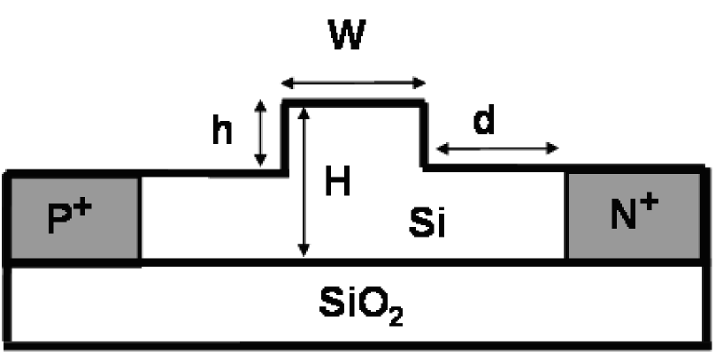
A schematic of the device is shown in Fig. 1. Devices were fabricated by standard optical lithography, dry etching, dopant implantation, passivation, and metallization techniques. Different variations of waveguide widths (W =1.5 to 3.0 m) and spacing between doped region wells and ridge edges (d =1.6 to 2.8 m) were obtained. Laterally-tapered mode-converters were fabricated in order to decrease the coupling loss into and out of the waveguides. The facets were polished but left uncoated. The best experimental results, presented in the following, are for 3-cm long waveguides (including the tapers) with W=1.5 m and d=2 m. A linear propagation loss of 0.5 dB/cm is measured in these waveguide using the Fabry-Perot technique.
The pump laser is a New Focus external-cavity tunable diode at 1539 nm with a linewidth of 0.1-0.2 nm amplified with an EDFA. The Stokes signal is a 1673 nm DFB laser biased at an output power of 4.5 mW. The pump and Stokes beams are coupled in and out of the waveguide with two identical objective lenses (M=20X, 0.40 NA), after combining the two beams in a wavelength division multiplexing coupler. Also, a 5/95 tap coupler is incorporated into the pump optical path to measure its power. The electrical loop that biases the diode consists of a power supply, a 1 k series resistor and a current meter. Unlike previous reports by us and others,11,12,15 no thermoelectric cooler was required to stabilize the device temperature.
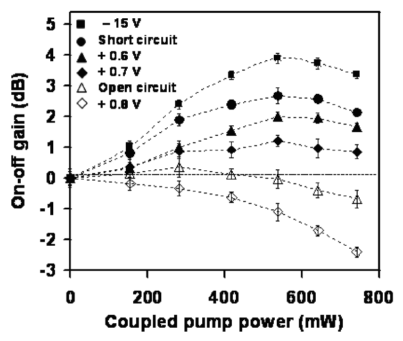
Figure 2 presents the measured on-off Raman gain at different coupled pump powers and biasing conditions. Although TPA of the pump power is not a major detriment by itself,10 the generated free carriers increase the loss substantially, preventing Raman gain in silicon waveguides.13 This is in agreement with the optical loss observed in Fig. 2 for an open-circuit p-i-n junction. When a reverse bias is applied, the induced electric field removes the TPA-induced free carriers from the waveguide region, hence reducing the carrier effective lifetimes. A maximum on-off gain of 4 dB is obtained at a reverse bias of 15 V. Considering the measured linear loss of 0.5 dB/cm, the highest achievable net Raman gain is thus 2.5 dB in the 3-cm long device. Higher reverse voltages do not increase the gain considerably, which may be due to saturation of the drift velocity. This argument is supported by the fact that for a p- and n-well separation of 5.3 m in the device, the average electric field at 15 V is equal to the peak electric field value of 3 V/cm in silicon. It is also observed that an on-off Raman gain of 2.7 dB is attained when the diode is short-circuit (0 V). This corresponds to a net Raman gain of 1.2 dB, which is higher than our previous report at zero bias where no lateral mode-converting tapers was involved.15
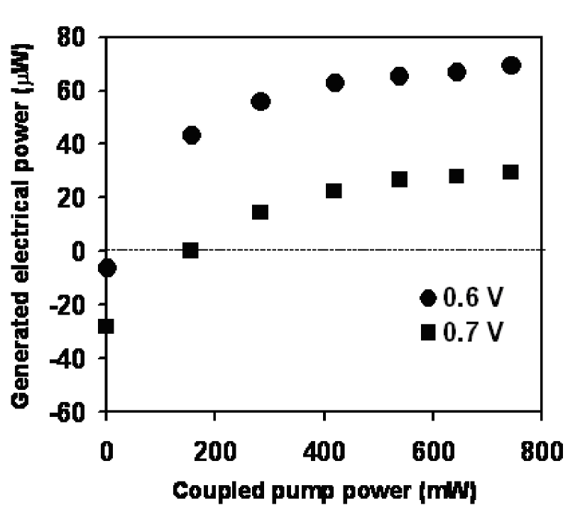
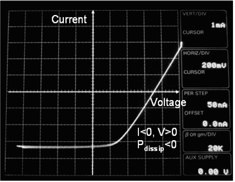
As seen in Fig. 2, on-off Raman gains as high as 2 dB is measured when the device is forward-biased at voltages 0.7 V. The importance of this biasing regime is that power dissipation is negative. Figure 3 shows the generated power for biases of 0.6 and 0.7 V at different pump intensities, extracted from the measured current and voltage drop across the diode. The TPA-induced photovoltaic effect is also clearly evident in the measured I-V characteristics presented in Fig. 4. The attenuated pump intensity via TPA creates free carriers in the SOI waveguide. The collected photogenerated carriers contribute to a current component that delivers electrical power to the external circuitry. Therefore, the sweep-out of TPA generated free carriers can be exploited to generate electrical power.
Sweep-out of carriers and reduction of the effective lifetime has been the motivation for utilizing a reverse-biased p-n junction in Raman amplifiers.10-13 The forward-bias employed in the present work might seem counterintuitive. However, it should be reminded that reduction of the effective lifetime can be achieved as long as the diode current is negative. In other words, a negative voltage is not a prerequisite for carrier sweep-out. We conducted 2-D numerical drift-diffusion simulations on structures identical to the fabricated devices using ATLAS (from Silvaco International), according to a methodology described elsewhere.14 It was verified that the effective lifetime of biases in the fourth quadrant is about one order of magnitude lower than the open-circuit value. Therefore, collection of photogenerated carriers in the fourth quadrant of the I-V characteristics by the built-in field can sufficiently decreases the free carrier loss and results in CW optical gain.
We now discuss the main limitation of the proposed approach. At very high optical intensities, the built-in field of the junction is insufficient to remove the high density of TPA-generated carriers. In such cases, a reverse bias needs to be applied to increase the field resulting in positive electrical power dissipation. Therefore, there exists a tradeoff between the amount of gain (and hence output power) and the electrical power generation/dissipation.
Finally, high pump intensities, and hence TPA, are also encountered in other silicon photonic devices that operate based on third-order nonlinear effects such as Raman lasers9,12 as well as in Raman and Kerr-based wavelength converters.16-18 Hence, the present approach is also applicable in these devices.
In conclusion, two photon absorption and the resulting free carrier scattering are omnipresent problems in silicon photonic devices that operate based on nonlinear optical interactions. It is shown that active removal of these carriers can be achieved while generating modest amount of electrical power.
This work is sponsored by DARPA under the EPIC program.
References
1R. A. Soref, Proceedings of IEEE 81, 1687 (1993).
2L. Pavesi and G. Guillot, Optical interconnects: the Silicon approach, Springer Series in Optical Sciences, (Springer, 2006; ISBN: 3540289100).
3D. J. Frank, IBM J. Research and Development 46, 235 (2002).
4International Technology Roadmap for Semiconductors, 2005 Edition,
http://www.itrs.net/.
5R. Claps,D. Dimitropoulos, Y. Han, and B. Jalali, Opt. Express 10, 1305 (2002).
6R. Claps,D. Dimitropoulos,V. Raghunathan,Y. Han, and B. Jalali, Opt. Express 11, 1731 (2003).
7R. L. Epinola, J. I. Dadap, R. M. Osgood, Jr., S. J. McNab, and Y. Vlasov, Opt. Express 12, 3713 (2004).
8X. Qianfan, V. R. Almeida, and M. Lipson, Opt. Express 12, 4437 (2004).
9O. Ozdal and B. Jalali, Opt. Express 12, 5269 (2004).
10T. K. Liang, H. K. Tsang, Appl. Phys. Lett. 84, 2745 (2004).
11A. Liu, H. Rong, M. Paniccia, O. Cohen, and D. Hak, Opt. Express 12, 4261 (2004).
12H. Rong, R. Jones, A. Liu, O. Cohen, D. Hak, A. Fang and M. Paniccia, Nature 433, 725 (2005).
13R. Claps, V. Raghunathan, D. Dimitropoulos, and B. Jalali, Opt. Express 12, 2774 (2004).
14D. Dimitropoulos, S. Fathpour, and B. Jalali, Appl. Phys. Lett. 87, 261108 (2005).
15S. Fathpour, O. Boyraz, D. Dimitropoulos, and B. Jalali, IEEE Conf. on Lasers and Electro-optics, CLEO 2006, Long Beach, CA (2006).
16R. Claps, V. Raghunathan, D. Dimitropoulos, and B. Jalali, Opt. Express 11, 2862 (2003).
17R. Espinola, J. Dadap, R. Osgood, Jr., S. McNab, and Y. Vlasov, Opt. Express 13, 4341 (2005).
18H. Fukuda, K. Yamada, T. Shoji, M. Takahashi, Tai Tsuchizawa, T. Watanabe, J. Takahashi, and S. Itabashi, Opt. Express 13, 4629-37 (2005).
Figure Captions
FIG. 1. Schematic of the fabricated silicon-on-insulator electrooptic modulator consisting of a p-n junction straddling the waveguide with H=2.0 and h=0.9 m. Values of d and W are described in the text.
FIG. 2. Measured on-off Raman gain versus coupled pump power in the devices of Fig. 1 at different biasing conditions.
FIG. 3. Generated electrical power at different coupled pump powers for two biases in the fourth quadrant.
FIG. 4. Current-voltage (I-V) characteristics of the diode measured with a curve-tracer for an input (uncoupled) optical illumination of 1.1 W.