Enhancing the photomixing efficiency of optoelectronic devices in the terahertz regime
Abstract
A method to reduce the transit time of majority of carriers in photomixers and photo detectors to ps is proposed. Enhanced optical fields associated with surface plasmon polaritons, coupled with velocity overshoot phenomenon results in net decrease of transit time of carriers. As an example, model calculations demonstrating (or 2800 and 31.8 W at 1 and 5 THz respectively) improvement in THz power generation efficiency of a photomixer based on Low Temperature grown GaAs are presented. Due to minimal dependence on the carrier recombination time, it is anticipated that the proposed method paves the way for enhancing the speed and efficiency of photomixers and detectors covering UV to far infrared communications wavelengths (300 to 1600 nm).
Recent experimental observation of extraordinary optical transmission through a normal metal film having subwavelength holesEbbesen has generated intense interest in harnessing the underlying physics for photonic applications. It is widely believed that quasi two-dimensional electromagnetic excitations tightly bound to the metal surface known as Surface Plasmon Polaritons (SPPs) are responsible for the observed near field enhancement of the optical radiation. Exponential decay of field components arising from SPPs (penetrating 100, 10 nm in dielectric and metal respectively), make them highly attractive for miniature photonic circuits and devicesBarnes . Currently, several potential applications of SPPs are being explored including wave guidingBozhevolnyi and near-field microscopyFurukawa . However, application of SPPs to enhance the speed and efficiency of photo detectors or photomixers has not been attempted due to the complexity of underlying physics and optimal device designs involving complicated dielectric-metal structures.
In this letter we propose a simple interdigitated metal structure embedded in a suitable semiconductor material to harness SPPs for improving the speed and efficiency of photomixers and detectors. Such a device can be realized with the existing material growth techniquesHarbison . As an example, we demonstrate via model calculations, significant () improvement in the efficiency of a THz photomixer based on Low Temperature grown GaAs (LT-GaAs). Microwave to THz radiation sources in the 0.1 to 10 THz are being extensively studied for their application in communications, medical imaging, and spectroscopyBjarnason ; Mittleman ; Pearson ; Woodward ; Kawase . For many applications- compact, narrow-linewidth, widely tunable continuous wave sources are necessary. In particular, to be used as a local oscillator in communications systems the THz source should produce stable output power WPearson ; Ito . Among the various techniques being pursuedBjarnason ; Pearson ; Ito ; Dohler ; Kohler electrical down conversion of optical microwave sources in a suitable photomixerBjarnason ; Ito ; Dohler are appealing due to the easy availability of tunable, narrow-linewidth, and stable solid state lasers. However, until now the output power from these photomixers is limited to W in the crucial THz range. In a conventional Metal-Semiconductor-Metal (MSM) photomixerBrown , optically thick ( 100 nm) interdigitated metal lines are fabricated on a high resistivity semiconductor with subpicosecond recombination time of carriers ( for electrons/holes respectively) and high breakdown field limit. So far, only a few materials such as LT-GaAsBjarnason ; Brown and Fe implanted InGaAsSuzuki have been shown to meet these requirements. From the photomixer theory, when two lasers (wavelengths , , and powers ) with their difference frequency in the THz range are incident on a dc biased photomixerBrown , the THz wave output power is given by
| (1) |
where is the photocurrent generated in the external circuit, is velocity of light in free space, is the capacitance, is small internal resistance of the metal structure, and is the load resistance in the 72-200 rangeBjarnason ; Dohler ; Brown . To accelerate carriers generated deep inside the semiconductor, high dc voltage ( V) is applied across the electrodes. This results in fields quickly exceeding the breakdown limit near the electrodes leading to device failure. As the carrier transport is transit time () limited, i. e., , recombination time is required to recombine the carriers that do not contribute to before the beat cycle reversesDohler ; Brown . Even if the photomixer is placed in a suitable optical cavity, due to strong reflection from thick metal electrodes, no carriers are generated directly below the electrodes where will be small. In addition, subwavelength features of the metal lines produce strong near field diffraction patterns that are not taken into account in conventional designsBjarnason ; Dohler ; Brown .
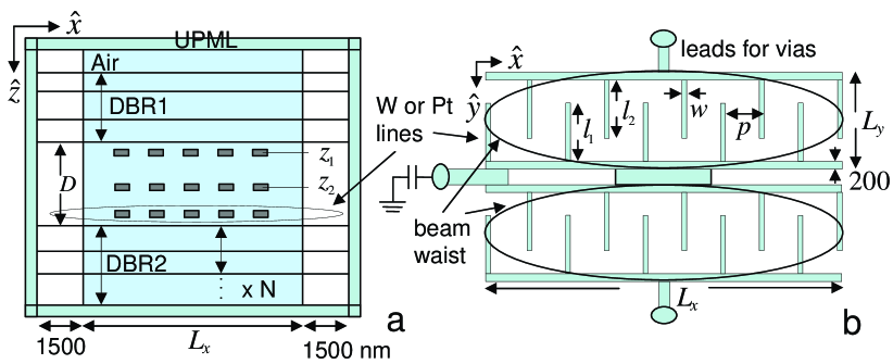
In the present technique, we exploit SPPs for generating more carriers close to subwavelength normal metal electrodes embedded in a photoconductor layer sandwiched between two Distributed Bragg Reflectors (DBR) that form a Fabry-Perot (FP) cavity. When coupled with velocity overshoot phenomenon reported in many photoconductor materialsDohler ; Betz ; Awano ; Reklaitis ; Thobel ; Foutz , of majority of carriers is reduced to 1 ps, i.e., . For efficient use of SPPs, it is desirable to have thin (10 nm) normal metal lines with subwavelength features distributed throughout the active volume (Fig 1a) in a manner that would collectively enhance the optical field intensity in the vicinity of the metal lines. This must however be accomplished without significantly increasing and . We show that for the proposed structure (Fig 1) optimized for 850 nm, is 2800 and 31.8 W at and 5 THz respectively. A convenient way to model such a complex structure is to solve the Maxwell’s equations with appropriate boundary conditions using Finite Difference Time-Domain (FDTD) formulationYee ; Taflove ; Sadiku . A 3D-FDTD simulator with Uniaxial Perfectly Matched Layer (UPML)Taflove surrounding the photomixer is developed for this purpose. Along the z-axis, the active volume consists of a few hundred nm of free space followed by DBR1, absorbing region with complex structure of normal metal electrodes, and pairs of low/high refractive index layers constituting DBR2 (Fig 1a)Park . For a given , the refractive index and thickness of DBR layers are first optimized by calculating the reflection and transmission coefficients of the FP cavity using matrix methodsHeavens . The FP cavity is excited by a linearly polarized, plane wave propagating along direction, with gaussian (elliptic) intensity profile in the plane. The source plane is placed in the free space above the DBR1. Frequency-domain Lorentz dispersion modelJudkins is adapted for metals with negative dielectric constant such as W or Pt.
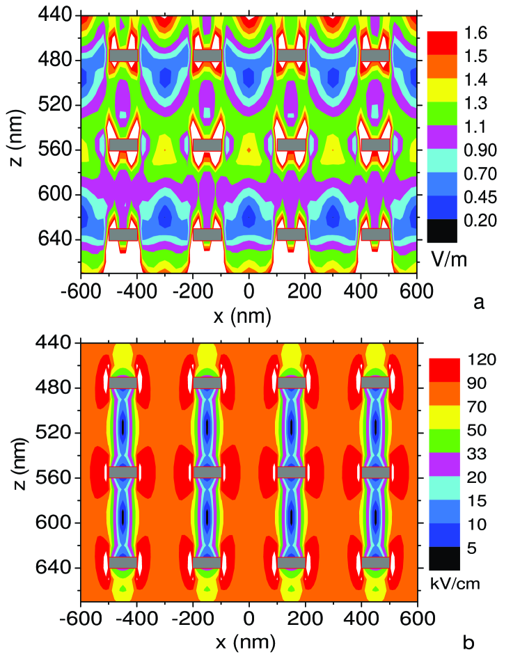
Figure 2a shows the FDTD results of a three layer stack of interdigitated W lines embedded in 230 nm LT-GaAs absorbing layer of a photomixer design of Fig 1 optimized for nm. The plot clearly shows the near field enhancement resulting from the thin normal metal electrodes. In the absence of the W electrodes, we obtain electric field amplitude maxima (maximum amplitude 1.4 V/m) corresponding to three antinodes in the standing wave formed between the DBRs. The 3D internal dc electric fields and are computed by solving Laplace’s equation with appropriate boundary conditions using FD techniquesSadiku . Figure 2b shows the contour plot of the static electric field strength within the LT-GaAs layer. The data show that unlike the traditional MSM structure, the field strength in this design is well above the critical field (5 kV/cm). Moreover, the field strength is 90 kV/cm between neighboring electrodes, in particular at the center of the device where most of the carriers are generated due to gaussian intensity profile of the incident laser beams. In the rest of the volume it has a broad peak at 18 kV/cm (not shown). Results show that fF and based on the resistivity of thin annealed or epitaxial W films (cm)Elbaum . The highest electric field inside the device is about four times lower than the breakdown field (500 kV/cm); therefore device failure due to electric breakdown is unlikely for this V.
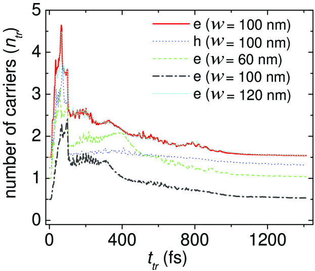
Photocurrent is calculated by first computing the electron/hole transit time distributions shown in Fig 3 for the entire absorbing volume based on the above FDTD and FD calculations. From the data available in literature for GaAs and LT-GaAs, for 100 fs, the carrier motion can be approximated by ballistic transport with electron effective mass , where is electron rest mass. This value is consistent with the slope of the linear portion of transient drift velocity curve obtained from Monte-Carlo calculationsReklaitis . The corresponding effective mass for holes is . Effective masses larger than the accepted values for GaAs (0.063, 0.076 for electron and light holes respectively) are considered so that longer , thereby lower estimate of results from these calculations. In the photomixer of Fig 2, pure ballistic transport is applicable to electrons generated close to the +ve electrodes and holes generated close to -ve electrodes. These carriers generated predominantly in the near field enhancement region, transit through non-uniform dc fields in the 5 to 90 kV/cm range. It should be noted that 100 fs is considerably lower than the theoretical limit of ballistic motion in GaAs for this field strength rangeBetz . For , electron motion is approximated by qasiballistic transport with time dependent velocity distribution similar to ref. 18 up to ps, and equilibrium drift velocity ( cm/s) for 3 ps. Hole motion is approximated by one third of the electron velocity at any given resulting in velocities lower than those reported for GaAsAwano .
The integral of curves in Fig 3 give the carriers ( for electrons and holes respectively) generated per period ( fs) of the 850 nm source with mW. For the parameters of Fig 2, 98% of incident power is absorbed in LT-GaAs layer while has peaks at 65 and 70 fs for electrons and holes respectively (solid red and dotted blue curves). Such a sharp peak followed by several satellite peaks and a long tail of the distribution can be understood from the fact that most of the carriers are generated close to the electrodes in the near field enhancement regions where the static fields are also strong. The satellite peaks result from periodicity of the electrode structure and specific choice of the velocity distribution. As 1 ps for majority of carriers in Fig 3, is not a critical factor in determining the performance at THz frequencies. A sharp drop in by a factor of 2 for electrons and a factor of 3 for holes at is due to the lower estimate of carrier velocities for resulting from the uniform field qasiballistic distribution functionReklaitis applied to a case where fields are inherently inhomogeneous. Although, the above choice of velocity distribution for quasiballistic motion is consistent with the fact that over a large volume fraction of the absorbing layer the static field is 18 kV/cm (not shown), a rigorous calculation should include quasiballistic velocity distribution appropriate for inhomogeneous fields. This would require ensemble Monte Carlo and carrier trajectory calculations carried out simultaneously. However, above calculations are adequate for obtaining the lower limit of the THz power output because a rigorous calculation would probably produce a more uniform distribution around without altering the distribution for or the integral of . This will further reduce the number of carriers in the long tail of the distribution.
Based on above distributions, the number of electrons captured in the metal electrodes at time will be
| (2) |
where is the number of electrons generated in LT-GaAs layer per second and is the carrier creation time. Similar expressions can be written for number of holes captured and the electrons/holes available for conduction in the photomixer . In the calculation of ( is electron charge), and , we set Brown , and varied in the 0.5 to 6 ps range. For the parameters of Fig 2, the steady state electron density obtained from the dc value of for ps is cm-3 (at 60 mW) with holes 1.5 times more numerous than electrons. We estimated that dipole fields arising from this space charge are negligible ( 2.5%) in comparison to strong fields (Fig 2b) present in the photomixer.
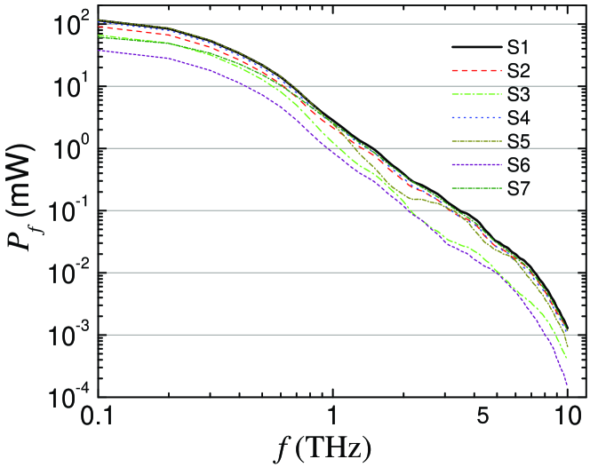
We have carried out calculations for over 70 configurations by systematically varying , polarization of the lasers ( or ), orientation of interdigitated lines in different layers, and DBR parameters. Fig 4 shows the values obtained from Eq 1 and 2 for some of the configurations in the 0.1 to 10 THz range. The data shows that in the 0.5 to 6.5 THz range in contrast to roll-off of for a conventional photomixerBrown . A recent nip-nip photomixer concept is shown to have roll-off for 1.5 THzDohler . Therefore, the design of Fig 1 exploiting SPPs offers significant improvement over the existing photomixer designs. Based on 3D FD computation of steady-state heat equation with appropriate thermal boundary conditions for the device parameters of Fig 2 ( mW, V), internal temperature () of the device is estimated to be 200 K above the substrate temperature requiring substantial cooling (to 77 K) when is high. Thermal conductivity () of various DBR layers and that of LT-GaAs are approximated by assigning 46 Wm-1K-1 and 10 Wm-1K-1, where are in-plane/out-of-plane conductivities. This internal heating therefore limits to 60 mW. However, the structure of Fig 1b, which is equivalent to two capacitors in series coupled to the antenna or transmission line, offers an alternative. If it is excited by TEM01 mode lasers with total power 120 mW as shown, the output can be increased to 2 (of Fig 4) without worsening or . To demonstrate the applicability of this method to other semiconductor materials, similar calculations are carried out for two more photomixers based on Be doped In1-xGaxAs and GaN optimized for operation at 1550 and 343 nm respectively. Both structures show strong near field enhancement arising from SPPs similar to Fig 2a and further work is underway to calculate the device efficiencies. Author wishes to thank John Goodkind for introducing him to the fascinating subject of Auston switches.
References
- (1) T. W. Ebbesen, H. J. Lezec, H. F. Ghaemi, T. Thio, and P. A. Wolff, Nature 391, 667 (1998).
- (2) W. L. Barnes, A. Dereux, and T. W. Ebbesen, Nature 424, 824 (2003).
- (3) S. I. Bozhevolnyi, V. S. Volkov, E. Devaux, and T. W. Ebbesen, Phys. Rev. Lett. 95, 046802 (2005).
- (4) H. Furukawa and S. Kawata, Opt. Commun. 148, 221 (1998).
- (5) J. P. Harbison, D. M. Hwang, J. Levkoff, and G. E. Derkits Jr., Appl. Phys. Lett. 47, 1187 (1985).
- (6) J. E. Bjarnason, et al., Appl. Phys. Lett. 85, 3983 (2004).
- (7) D. M. Mittleman, R. H. Jacobsen, and M. C. Nuss, IEEE J. Select. Top. Quant. Electron. 2, 679 (1996).
- (8) J. C. Pearson et al., Proc. SPIE 5498, 486 (2004).
- (9) R. M. Woodward, V. P. Wallace, D. D. Arnone, E. H. Linfield, and M. Pepper, J. Biol. Phys. 29, 257 (2003).
- (10) K. Kawase, Y. Ogawa, and Y. Watanabe, Opt. Express 11, 2549 (2003).
- (11) H. Ito, F. Nakajima, T. Furuta, and T. Ishibashi, Semicond. Sci. Technol. 20, S191 (2005).
- (12) G. H. Dohler et al., Semicond. Sci. Technol. 20, S178 (2005).
- (13) R. Kohler et al., Nature 417, 156 (2002).
- (14) E. Brown, Appl. Phys. Lett. 75, 769 (1999).
- (15) M. Suzuki and M. F. Tonouchi, Appl. Phys. Lett. 86, 051104-3 (2005).
- (16) M. Betz et al., Semicond. Sci. Technol. 19, S167 (2004).
- (17) Y. Awano, Y. Tagawa, and M. Shima, IEEE/Cornell Conference on Advanced Concepts in High Speed Semiconductor Devices and Circuits, Proceedings., 408 (1995).
- (18) A. Reklaitis, A. Krotkus and G. Grigaliunaite, Semicond. Sci. Technol. 14, 945 (1999).
- (19) J. L. Thobel, L. Baudry, A. Cappy, P. Bourel, and R. Fauquembergue, Appl. Phys. Lett. 56, 346 (1990).
- (20) B. E. Foutz, L. F. Eastman, U. V. Bhapkar, and M. S. Shur, Appl. Phys. Lett. 70, 2849 (1997).
- (21) M. Wraback, H. Shen, S. Rudin, and E. Bellotti, Phys. Stat. Sol. (B) 234, 810 (2002).
- (22) K. S. Yee, IEEE Trans. Ant. Prop. AP-14, 302 (1966).
- (23) A. Taflove and S. C. Hagness, Computational Electrodynamics - The Finite Difference Time-Domain Method(Artech House Publishers, Norwood, MA).
- (24) Y. Park et al., Appl. Phys. Lett. 82, 2770 (2003).
- (25) O. S. Heavens, Rep. Prog. Phys. 23, 1 (1960).
- (26) J. B. Judkins and R. W. Ziolkowski, J. Opt. Soc. Am. A 12, 1974 (1995).
- (27) Numerical Techniques in Electromagnetics 2nd Ed. by M. N. O. Sadiku, CRC Press, Washington D.C., USA.
- (28) L. K. Elbaum, K. Ahn, J. H. Souk, C. Y. Ting, and L. A. Nesbit, J. Vac. Sci. Technol. A 4, 3106 (1986).