Concept, realization and characterization of serially powered pixel modules (Serial Powering)
Abstract
We prove and demonstrate here for the example of the large scale pixel detector of ATLAS that Serial Powering of pixel modules is a viable alternative and that has been devised and implemented for ATLAS pixel modules using dedicated on-chip voltage regulators and modified flex hybrids circuits. The equivalent of a pixel ladder consisting of six serially powered pixel modules with about 0.3 Mpixels has been built and the performance with respect to noise and threshold stability and operation failures has been studied. We believe that Serial Powering in general will be necessary for future large scale tracking detectors.
, , ,
1 Introduction
Modern particle detectors require on the one hand a large solid angle coverage and high granularity, on the other hand fast read-out and low power consumption. Especially particle trackers require in addition a minimum of passive material inside their active region. The high granularity results in building a detector from a large number of identical active modules. The usual power scheme is the individual, parallel powering of the modules with a constant voltage. However, this is disadvantageous for a large scale detector such as a pixel detector.
The pixel detector as the innermost sub-detector of many large scale particle detectors has a very high granularity. The ATLAS pixel detector comprises 1744 active pixel modules containing about 80 million channels [2]. It makes use of deep sub-micron (0.25) chip technology for the read-out which is necessary to achieve a radiation tolerant, compact, and high granularity detector design. Each hybrid module is composed of a 250 thick silicon sensor and 16 Front-End chips with a total of approx. 46 000 pixels with a size of .
In order to achieve a fast operation of the detector, the electronic circuits must be powered with high currents (approx. ) at low voltages (1.6 analog, 2.0 digital). Therefore a high power density of the detector comes with the high granularity. Since the power supplies are located outside the active detector volume, the power is transmitted over a long distance (which can easily attain ) and the voltages are regulated remotely from outside the active volume of the detector (for a large scale detector the distance can be larger than 10). Further, the power cable diameter is small inside the detector volume (typically diameter Al wires). Together with the low voltages and high currents the power losses in the cables exceed the actual power consumption of the modules. Moreover, the further the granularity increases, the more cables are needed. This results not only in an increase of the power losses, but also increases the passive material in the active detector volume. Hence, from a certain granularity onwards the parallel powering concept has more and more disadvantages and it will become more favorable to change to the new serial powering scheme.
For the Serial Powering concept [1] a chain of modules is powered in series by a constant current. Only two power lines per chain are needed. The voltages are generated by shunt and linear regulators implemented on the chip itself (see figure 1). Serial Powering offers a drastic reduction of power lines and therefore a reduction in passive materials in the active detector region as well as a reduction of power losses in the cables. A positive side effect is the reduction of the heat from the power lines that can uncontrollably heat up other detector systems.
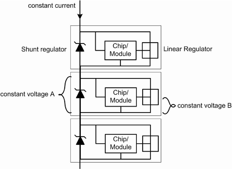
In this paper we demonstrate for the ATLAS Pixel Detector that Serial Powering is a viable alternative for a possible upgrade of the ATLAS Inner Detector and that all the possible problems listed in the next section, concerning stability and reliability, can be solved if a dedicated Serial Powering design is used.
2 Example calculation on the ATLAS pixel detector
Every module is connected to 8 power cables, i.e. two power lines and two sense lines for every voltage. The total voltage drop from the power supplies in the control room to the module is 6.4 and the power losses in the cables are maximum. This is times of the power consumption of the 13 modules. The total lengths of all cables in the active region are , this corresponds to an average radiation length of 0.073 %.
Since the modules of the pixel detector are organized in 114 pixel ladders (staves) with 13 modules, this suggests that the 13 modules of such a stave form a chain of serially powered modules. The advantages of a serially powered chain of 13 modules follow from an example calculation (table 1):
-
-
Passive material, i.e. power cables in the detector is reduced by a factor of 50 compared to the Parallel Powering scheme. This corresponds to 15% of the radiation length of the parallel scheme.
-
-
Power losses in the cables are reduced by a factor 10.
-
-
Reduced power losses in the cables also reduce heat-pick up by other detector systems.
-
-
Voltage regulation is done on-chip, i.e. close to the consumer. The regulation can respond faster to voltage changes due to varying power consumptions.
| Parallel | Serial | Factor | |
|---|---|---|---|
| Power supplies | 13 | 1 | 13 |
| No. of power lines | 104 | 2 | 52 |
| Total cable length (mm) | 121160 | 2780 | 43.6 |
| radiation length per layer | 0.073 % | 0.011 % | 6.5 |
| Cable power losses | 191 W | 19.2 W | 9.97 |
| Module (Shuntreg. 2.0 V) | 67.9 W | 78 W | 0.87 |
| Module (Shuntreg. 2.7 V) | 105.3 W | 0.65 | |
| Sum (Shuntreg. 2.0 V) | 259 W | 97.2 W | 2.67 |
| Sum (Shuntreg. 2.7 V) | 124.5 W | 2.08 |
Apparently also several concerns about Serial Powering arise. The first concern that the local power consumption of the module is higher than for parallel powered modules can be rejected partially from a separate calculation which includes the total heat load for the cooling system. The heat load from the cables111The heat load per cable is approx. . that are closest to the module is transferred to the modules and the decrease of the heat load due to less cables counterbalances the increase of the module heat. The heat that must be cooled by the cooling system decreases by 7% (Serial Powering scheme with 2.0 voltage drop across a module) or increases maximally by 17% (scheme with 2.7 voltage drop across a module). Additionally, the heat is now produced close to the cooling and as mentioned above there is less heat pickup by other detector systems, so that the slight increase of the heat load has overall positive effects on the detector.
3 General Serial Powering Scheme
There are three shunt regulators on the ATLAS pixel production chip, DSHUNT, AOVER and DOVER that have design threshold voltages of 2.0, 2.4, and 2.7, respectively. The two linear regulators ALINREG and DLINREG have adjustable output voltages in four steps from 1.5 to 1.8 or 1.8 to 2.4, resp. Both regulators are described in detail in [1] [4] and [6]. The different powering schemes are realized by proper connections between the input pads of the different regulators on the chip (figure 2 show the schematically the powering components of a chip).
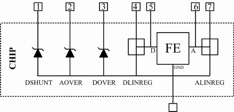
Figure 3 shows a chain of serially powered modules (Extended Serial Powering scheme [1], by connecting pad 3, 4 and 7 in figure 2 to the constant current source). A constant current source is connected to the power input of the first module. The ground of the module is then connected to the power input of the next module etc. The current consumption is determined by the highest current consumption of one module in the chain. The supply voltages of the chips are generated by the two types of regulators. One is a shunt regulator which behaves like a Zener diode. The other one is a linear voltage regulator.
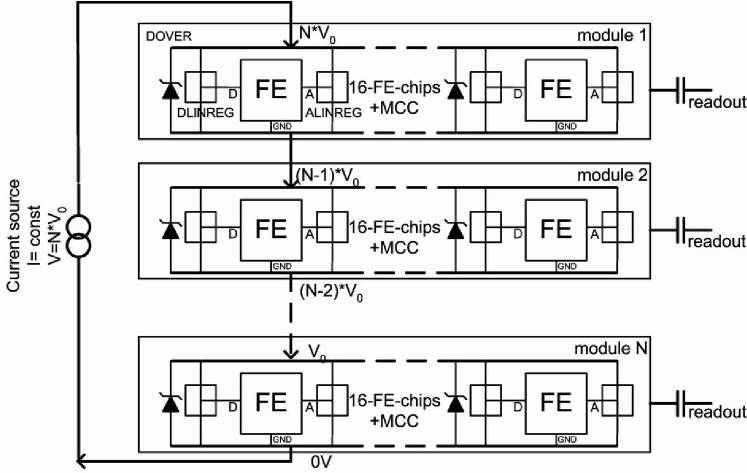
On a module the shunt regulators of all 16 chips are connected in parallel. This stabilizes the output voltage. The fear of a loss of a whole module chain is also addressed this way. The redundant use of the shunt regulators can maintain the voltage regulation and the chain remains uninterrupted even if one or more regulators should break (i.e. creates an open-circuit). Thus the risk of loosing a whole chain is minimized. The common output voltage of the shunt regulators is the input voltage for the two linear regulators of every chip. The outputs of the regulators are already internally connected to the analog and digital part, respectively. The suitable regulators for this scheme are therefore the two linear regulators that are powered by the DOVER regulator. As the modules now have different ground potentials, the read-out must be done via AC coupling of the signals (as indicated in figure 3 by a symbolic capacitor).

One alternative Serial Powering schemes can also be considered. The Simple Serial Powering scheme (fig. 4 by connecting pad 1, 5 and 7 to the constant current source) uses the DSHUNT regulator to power the digital part and the analog linear regulator. In this scheme the total voltage which drops across a module is lowest (2.0) and therefore also the power consumption of a single module is the lowest. A disadvantage is that the digital voltage is fixed to the threshold voltage of the shunt regulator.
4 Operation of a serially powered module ladder
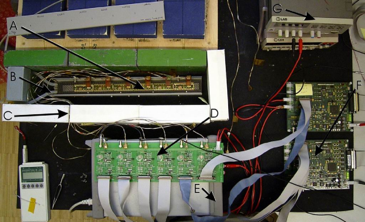
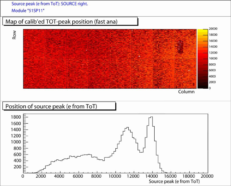
After testing and comparing single serially powered modules [1] [6], which were built with already existing ATLAS pixel chips and a dedicated flex-hybrid, six Serial Powering modules were composed to a ladder, a so called half-stave, containing about 0.3 . The measurement setup is shown in figure 5. The same original mechanical support structure for module ladders was used except for the reduced number of modules. The serial connections between the modules was made by original power cables (type-0) which were connected to a special board that routes the current serially through all modules. Additionally it AC-couples the LVDS signals between the modules and the external read-out electronics through a pair of capacitors and a LVDS buffer for each data line. The operation commands, i.e. commands that injects test charges into the pixels and initiates the read-out chain, could be sent to all modules at the same time. This emulates the situation in the detector when all modules are individually having digital and analog activities and varying power consumptions. As first qualitative proof of operation, figure 6 shows the spectrum of a point source placed above and between two modules and recorded simultaneously. Only shown is the left hit map which corresponds to the module that was on the left side of the source. In the spectrum two peaks can be seen. The peak at higher deposited charge is due to the absorbed 59.54-photon222The second peak results from gamma rays that transverse the sensor in an shallow angle so that charge is shared among two pixels. In one of the pixels the charge fraction is below the threshold. This results in a second peak which is shifted by threshold.. This tests the whole detection chain from the charge collection in the sensor, the hit processing in the chip to the output of the hit data. It is a qualitative proof of the full module functionality.
4.1 Performance Characterization
The performance of each module while serially powered with five other actively working modules was measured (multi-module operation mode). The measurements were repeated until all six modules were read out. Figure 7 shows the threshold maps and the noise maps of the six modules333Some modules are without sensor or with some defect chips because of cost reasons, still the vast amount of pixels can give a good impression of the module’s performance. and table 2 shows the threshold (THRES), threshold dispersion () and the noise performance of the six modules. The noise difference between the single serially powered operation (only one single active, serially powered module) and the multi-module operation mode is given in brackets. This is the first time that such a large chain of serially powered modules was powered and that all modules were operated at the same time. The results in comparison to singly serially powered operation and parallel powered modules show hardly any influence of the modules on each other during normal operations.

| Module | THRES () | () | noise () |
|---|---|---|---|
| M1 | 4134 | 57 | (4) |
| M2 | 4156 | 69 | 182 (-1) |
| M3 | 4173 | 70 | 186 (-0) |
| M4 | 4162 | 70 | 183 (-4) |
| M5 | 4132 | 58 | (0) |
| M6 | 4160 | 91 | 172 (-5) |
| Parallel | 4062 | 50 | 160 |
| + without sensor | |||
4.2 Failure Mode Studies
Two types of failures were studied in order to test the reliability of the Serial Powering scheme. The first was the study of the effect of a noisy module in the chain. This was achieved by lowering the detection threshold of one module to almost zero, so that this module sees noise hits all the time. That involves a permanent analog and digital activity as well as permanent changing current consumptions which can modulate the powering of the other modules by permanently changing the potentials across the modules. The measurement was repeated six times, so that each time a different module was made noisy and the effect on the other modules was investigated. Table 3 shows the noise difference of every module between the failure mode measurement and the normal operation. Each row is a different measurement with a different noisy module.
| Noisy module | M1 () | M2 () | M3 () | M4 () | M5 () | M6 () |
|---|---|---|---|---|---|---|
| Module 1 | — | 13 | 2 | 2 | 13 | 3 |
| Module 2 | 6 | — | 10 | 5 | 0 | 9 |
| Module 3 | 0 | 2 | — | 2 | 0 | 3 |
| Module 4 | 1 | 9 | 2 | — | 0 | 9 |
| Module 5 | 10 | 2 | 1 | 15 | — | 20 |
| Module 6 | 0 | 2 | 2 | 2 | 0 | — |
The increase in noise for neighboring modules in the chain is small (max. ) compared to the normal noise of to and it is well below the ATLAS requirement for the maximum noise. This shows that the filtering and the regulation of the supply voltages is sufficient enough to filter such a disturbance on the power lines.
The second type of failure mode tested is a noisy module emulated by an external switchable load connected in parallel to one module. The distortion was tuned to different frequencies up to 40. The load varied between 300 and 500. This constitutes a much more massive interference to the supply current than a noisy module. The effect on the chain is again a shift in potentials for all modules.
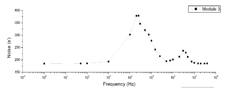
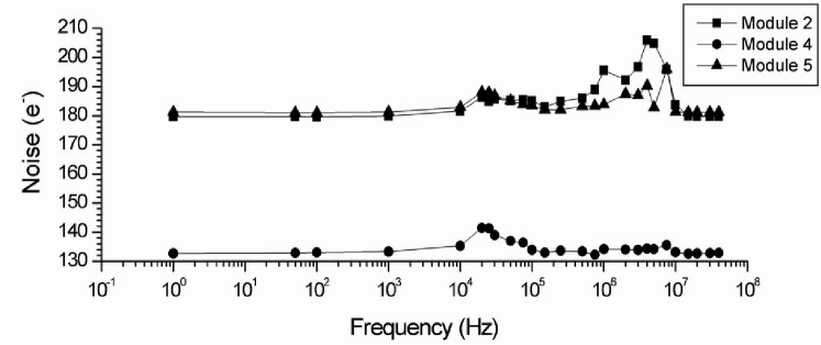
Figures 8 and 9 shows the frequency dependence of the noise of module 3 which was parallel to the switchable load. During the whole measurement module 3 could be configured and read out sequentially without any problems. Only in two regions around 25 and around 3 the noise rises to undesired values of 350 resp. 230. More important is to observe the effect on the other modules, whether neighboring modules pick up the higher noise from module 3. Figure 9 shows the frequency dependence of the noise of the three neighboring modules in the chain. Clearly the change in noise is small for all modules444module 5 is again without sensor. Therefore there is hardly any noise pick up by Serial Powering modules from noise on the power line. We consider this experimental test a very important demonstration that the Serial Powering scheme is reliable.
5 Summary
We have demonstrated that Serial Powering is a viable concept to provide operation power to a large pixel detector system such as the ATLAS pixel detector at LHC. A powering scheme that powers a chain of modules with a constant current and uses dedicated on-chip voltage regulators and modified flex hybrid circuits has been devised and implemented for ATLAS pixel modules.
An example calculation shows that such a chain of 13 modules offers a reduction in power losses of the cables by 90% and a reduction in passive materials by 98%, this is a reduction of 85% in radiation length. It has been shown that the spread in quality of the voltage regulators, as the key elements to this powering scheme, is sufficiently small and the voltage stability of the linear regulators is excellent, so that the voltage regulators are applicable for Serial Powering. The serially powered modules have been intensively tested in the lab. The comparison between parallelly powered and serially powered modules has shown no difference between the two powering schemes. Finally, the equivalent of a pixel ladder consisting of six serially powered pixel modules with about 0.3 Mpixels has been built and the performance with respect to operation failures has been studied. Measurements with artificially noisy modules mimicked by inducing noise on the power lines have only shown a marginal increase in noise of the other modules in the chain. We strongly believe that Serial Powering is not only a viable powering scheme for an upcoming upgrade of the ATLAS pixel detector, but is also viable, if not necessary for future large scale tracking detectors.
References
- [1] T. Stockmanns et al. Serial powering of pixel modules. Nucl. Instr. & Meth. A511 (2003) 174–179. and T. Stockmanns. Multi chip module development for the ATLAS pixel detector. PhD thesis BONN-IR-2004-12 (2004) (in German).
- [2] The ATLAS Pixel collaboration. ATLAS Pixel Detector, Technical Design Report. CERN/LHCC/98-13 (1998).
- [3] M. Olcese et al. Requirements for pixel detector services. ATLAS Internal Report ATL-IP-ES-0007 (2004).
- [4] I. Perić. Design and Realization of Integrated Circuits for the Readout of Pixel Sensors in High-Energy Physics and Biomedical Imaging. PhD thesis BONN-IR-2004-23 (2004).
- [5] J. Grosse-Knetter (for the ATLAS Pixel collaboration). The ATLAS Pixel Detector. in print at Nucl. Instr. & Meth. A, ref 1687.
- [6] D.B. Ta Development and Demonstration of Serial Powering on ATLAS Pixel Modules and Moduleladders (Fuctionality and Reliabilitytests) Diplomathesis BONN-IB-2005-04 (2005) (in German)
The thesis of the university of Bonn can be found under
hep1.physik.uni-bonn.de under the section
Publications.
This paper is a short version of the following paper:
D.B. Ta et al. Serial Powering: Proof of principle demonstration of a scheme for the operation of a large pixel detector at the LHC Nucl. Instr. & Meth. A557 (2006) 445–459.