Characterization of a CCD array for Bragg spectroscopy
Abstract
The average pixel distance as well as the relative orientation of an array of 6 CCD detectors have been measured with accuracies of about 0.5 nm and 50 rad, respectively. Such a precision satisfies the needs of modern crystal spectroscopy experiments in the field of exotic atoms and highly charged ions. Two different measurements have been performed by illuminating masks in front of the detector array by remote sources of radiation. In one case, an aluminum mask was irradiated with X-rays and in a second attempt, a nanometric quartz wafer was illuminated by a light bulb. Both methods gave consistent results with a smaller error for the optical method. In addition, the thermal expansion of the CCD detectors was characterized between C and C.
pacs:
07.85.Nc, 14.40.Aq, 29.40.Wk, 36.10.Gv, 39.30.%2Bw, 65.40.DeI Introduction
Charge–coupled devices (CCDs) are ideally suited as detectors for X–ray spectroscopy in the few keV range, because of excellent energy resolution and the inherent two-dimensional spatial information. In particular, they can be used as focal-plane detectors of Bragg crystal spectrometers for studies of characteristic X–radiation from exotic atoms with ultimate energy resolution Gotta (2004).
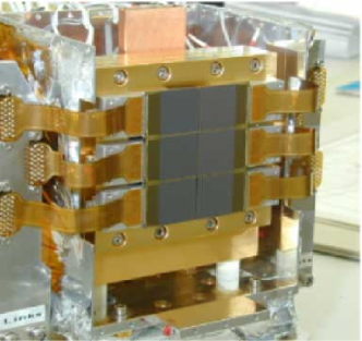
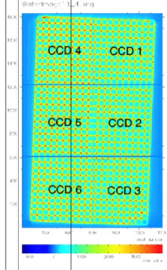
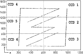
The detector described in this work was set–up for a bent crystal spectrometer used in three ongoing experiments at the Paul Scherrer Institut: the measurement of the charged pion mass Pion Mass Collaboration (1997); Nelms et al. (2002a), the determination of the strong–interaction shift and width of the pionic hydrogen ground state Pionic Hydrogen Collaboration (1998); Anagnostopoulos et al. (2003) and highly charged ion spectroscopy Trassinelli et al. (2005). The detector is made of an array of two vertical columns of 3 CCDs each Nelms et al. (2002b) (Fig. 1). Each device has square pixels with a nominal dimension of m at room temperature. Each pixel is realized by an open-electrode structure. For this reason, the dimension characterizing the detector is rather the average distance between pixels centers than the size of the individual pixel.
As the CCD is usually operated at C, the knowledge of the inter–pixel distance at the working temperature is essential for crystal spectroscopy, because any angular difference is determined from a measured position difference between Bragg reflections. Furthermore, for an array like the one described here, the relative orientation of the CCDs has to be known at the same level of accuracy as the average pixel distance.
A first attempt to determine the relative positions has been made using a wire eroded aluminum mask illuminated by sulphur fluorescence X–rays produced by means of an X–ray tube. The alignment of the mask pattern made it possible to estimate the relative CCD position with an accuracy of about 0.05 – 0.1 pixel and the relative rotation to slightly better than 100 rad Hennebach (2004). In order to obtain in addition a precise value for the average pixel distance a new measurement was set–up using a high-precision quartz wafer in front of the CCD illuminated with visible light. Using this method, the relative CCD devices’ position was evaluated with an accuracy of about 0.02 pixel. The temperature dependence of the pixel distance was also determined.
Section II is dedicated to the description of the optical measurement set–up. In section III, we describe the measurement of the pixel distance. Section IV we present the measurement of the CCD orientation using the aluminum mask (Sec. IV.1) and using the quartz mask (Sec. IV.2). In section V we describe the measurement of the inter–pixel distance temperature dependence.
II Set–up of the optical measurement
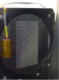
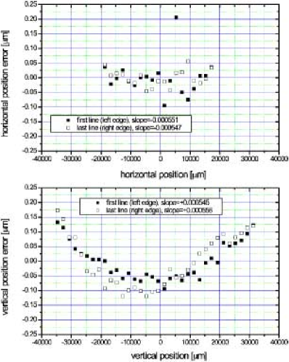
The quartz wafer is an optical cross grating manufactured by the Laboratory of Micro- and Nanotechnology of the Paul Scherrer Institut. The grating is 40 mm wide and 70 mm high. It is composed of vertical and horizontal lines of 50 m thickness separated from each other by 2 mm (Fig. 2). The linearity of the lines is of order 0.05 m in the horizontal direction. In the vertical direction, the lines become slightly parabolic with a maximum deviation of 0.15 m from the average value (Fig. 3).
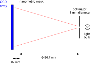
The wafer was positioned 37 mm in front of the CCD array. It was illuminated with short light pulses using a point–like light source, which was approximated by a collimator of one millimeter in diameter located in front of a light bulb at a distance of 6.43 m from the CCDs to reduce parallax effects distorting the wafer image (Fig. 4-5). The wafer temperature was monitored and remained at room temperature during the measurements. The integration time per picture was 10 s with the bulb shining for 6 s for each selected temperature of the CCDs. The temperature was varied between C and C.
III Measurement of the average pixel distance
For the determination of the pixel distance, a simultaneous linear fit of two adjacent lines was performed under the constraint that the two lines are parallel.
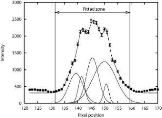
After cutting out the crossing points, the diffraction pattern of the straight sections linking them (zones) was fitted to a superposition of 5 Gaussian profiles: central peak, first and second side maxima, and left and right backgrounds (Fig. 6-7). The parabolic shape of the grating was taken into account in the analysis of the images recorded with the detector.
For the fit of two parallel lines we have to consider two sets of data at the same time: and , and the lines are described by the equations:
| (1) |
The best determination of the parameters , and is obtained by minimization of the merit function following the same procedure as described in Ref. Press et al. (2001). In this case, the merit function is:
| (2) |
Considering two parallel lines that are at a distance (in m) on the CCD, the average pixel distance is obtained from the formula:
| (3) |
The presence of the cosine term takes into account the fact that the lines are generally not parallel to the CCD edge. The detailed formulas for the minimization are presented in Appendix A.
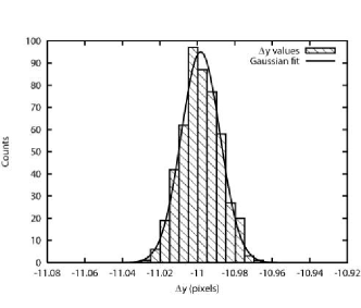
For each CCD, we obtained about 180 independent evaluations of the pixel distance from straight sections of different line pairs. The average value of the pixel distance was obtained by a Gaussian fit to the histogram obtained from individual values (Fig. 8-9). Two series of images were available and the final value was calculated from the sum of the two distributions.
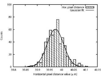
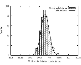
It is interesting to observe that the vertical and horizontal distributions have different dispersions (Fig. 8-9 and Table 1). The horizontal pixel distance distribution is characterized by a FWHM of 80 nm, compared to 50 nm for the vertical one. Accordingly, the error on the Gaussian peak position for the vertical distance is half that for the horizontal one (0.9 nm and 1.8 nm, respectively). We have no clear-cut explanation for this difference. It is unlikely that this difference could come from the accuracy of the mask fabrication. As seen from Fig. 3, the line distances show similar fluctuations in the order of 0.05 m for both directions and they should produce a dispersion of about 0.05 m / 50 = 1 nm on the vertical and horizontal pixel distance (50 is the average number of pixels between two lines in the wafer image).
The CCD devices were fabricated using a 0.5 m technology, which means that the uncertainty over the full size is 0.5 m (at room temperature). Such an inaccuracy could introduce an average difference of order 0.8 nm for the inter–pixel distance of various CCDs. This assumption was tested applying Student’s t-test Press et al. (2001) to distributions from different CCDs. The only significant difference in the obtained distributions comes from CCD 2 and CCD 5. However, for these two CCDs we observe a parasitic image of the mask superimposed on the normal one, probably due to a reflection between the detector and the mask itself. Therefore, the final value of the pixel distance is given by the weighted average of the individual CCD values excluding CCD 2 and CCD 5 (Table 1).
The overall precision of the quartz wafer is quoted to be mm over the full width of 40 mm. Hence, the uncertainty of the wafer grid contributes on average 0.1 m / 1000 = 0.1 nm per pixel. As horizontal and vertical pixel distances are in good agreement, a weighted average is calculated. Taking the wafer uncertainty of 0.1 nm into account, the average pixel distance reads , where the nominal value is 40.
| CCD | Hor. dist. (m) | FWHM (m) | |
| 1 | 1.11 | ||
| 2 | 1.26 | ||
| 3 | 1.41 | ||
| 4 | 1.16 | ||
| 5 | 1.01 | ||
| 6 | 1.20 | ||
| weighted average | without CCDs 2 and 5 | ||
| line fits | |||
| CCD | Vert. dist. (m) | FWHM (m) | |
| 1 | 1.05 | ||
| 2 | 0.88 | ||
| 3 | 0.68 | ||
| 4 | 0.62 | ||
| 5 | 0.52 | ||
| 6 | 0.66 | ||
| weighted average | without CCDs 2 and 5 | ||
| line fits | |||
IV Measurement of the relative orientation of the CCDs
IV.1 X–ray method
An aluminum mask was installed 37 mm in front of the CCD array; this mask has a slit pattern chosen to provide an unambiguous connection between all CCDs (Fig. 11). The mask has a thickness of 1 mm, the slits are wire eroded with a width of about 0.1 mm and the linearity is about 50 over the full height. The detector array, shielded by the mask, was irradiated with sulphur X–rays of 2.3 keV produced with the help of an X–ray tube; this energy is low enough to keep charge splitting effects small Anagnostopoulos et al. (2003). The sulphur target was placed at about 4 m from the detector. A collimator with a diameter of 5 mm was placed close to the target to provide a point–like source. In total, about 600 000 X-ray events were collected.

The relative rotations of the CCDs are determined by performing linear fits to sections of the mask slit images. Because of the slit arrangement, CCD 3 (CCD 6 would be equivalent) is the best choice to serve as reference frame. In this case, the relative rotations of CCDs 1,2 and 6 are established directly. The values for CCD 4 and CCD 5 are the weighted average of results with CCD 1 and CCD 6 as intermediate steps.
The fit is done by calculating the center of gravity (COG) for each CCD row (or column for fitting a horizontal line) and then making a linear regression through them. The error of the COGs is based upon a rectangular distribution with a width equal to the width of the slits of the mask. With N as the number of events and w as the slit width, . A width of 4 pixels for the horizontal/vertical lines and 6 pixels for the diagonals is assumed. From the inclinations (in mrad) of the mask slits relative to the perfect horizontal, vertical or diagonal (45∘), the rotations of individual CCDs are calculated. Results (relative to CCD 3) are given in Table 2.
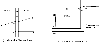
After the rotations have been determined and corrected for, the lines were fitted again to determine the crossing points of each slit with the CCD edge. The relative offsets and can be determined only if there are at least two lines crossing from one CCD to the other (Fig. 12). With CCD 3 as the starting point, the only other CCD fulfilling this condition is CCD 6. The position of all other CCDs has to be calculated relative to all CCDs shifted so far. The correct order for this is CCD 2, then CCD 5, CCD 1 and CCD 4.
The correct values for the vertical offsets follow from the condition that both lines should continue from one CCD to the other (CCD A and CCD B in Fig. 12). For case i) in Fig. 12, one horizontal and one diagonal line:
| (4) |
where are the y-coordinate of the crossing point between the lines of equation (constant) and the CCD edge. From this, one derives:
| (5) |
and the associate error is:
| (6) |
For case ii), one horizontal and one vertical line,
| (7) |
(note that is defined as (constant) ). Here, the equations are:
| (8) |
| (9) |
Values for are derived by inserting in either of the starting equations Eq. (4). The final horizontal and vertical displacements (which depend on the previously determined set of rotations) are given in Tab. 2.
The analysis of the mask data assumes that the slits on the mask are perfectly straight; the given uncertainties are then purely statistical. However, a detailed study of the vertical slit to the right (on CCD 1 to CCD 3) shows that the mechanical irregularities of the mask are big enough to be noticeable. Fig. 13 shows the centers of gravity calculated for this slit subtracted from the fit through these points. Both the sudden jump (left arrow) and the inclination change (right arrow) are substructures on a scale of roughly 1/10th of a pixel (4 m). This fits well with the mechanical accuracy of 5 m quoted for the mask slits. Consequently, a further improvement in accuracy is not limited by statistics, but by the mechanical precision of the mask itself. More details may be found in Hennebach (2004).

| CCD | (pixels) | (pixels) | (mrad) |
|---|---|---|---|
| CCD3-CCD1 | |||
| CCD3-CCD2 | |||
| CCD3-CCD3 | |||
| CCD3-CCD4 | |||
| CCD3-CCD5 | |||
| CCD3-CCD6 |
IV.2 Optical method
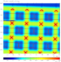
By using the nanometric quartz wafer, the precision for the CCD offsets was improved beyond 1/20 of the pixel width of 40 m, which was envisaged for measuring the charged pion mass. The knowledge of the line positions on the wafer allows one to infer the relative position between pairs of CCDs from the image. As for X–rays, the image, when visualized without position and rotation correction, shows discontinuities at the boundaries of adjacent CCDs: lines are not parallel and a part of the mask image is missing due to the spatial separation of the CCDs (Fig. 14 bottom–left). Again, one CCD has to be chosen as a reference.
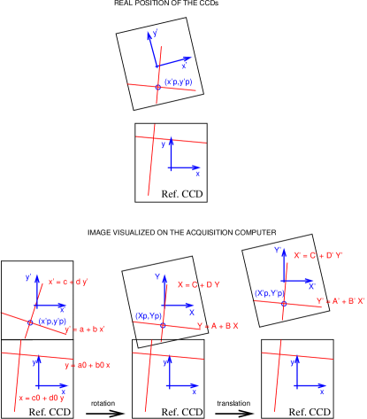
The unambiguous calculation of relative horizontal and vertical shift ( and ) and rotation () of two CCDs requires the information coming from at least one pair of perpendicularly crossing lines per CCD. Using the line parameters, it is possible to build a function depending upon , and , which is minimal when the shift and rotation values are optimal. The idea is to compare the coordinates of a crossing point using the reference frame of the reference CCD (, ) and of the selected CCD (, ). The values of and are unequivocally determined by first applying a rotation of the coordinate system of the selected CCD around the CCD center. The value of the rotation angle is chosen to have the lines parallel to the ones of the reference CCD (Fig. 14 bottom-middle side). In this new frame, the coordinates of the crossing point depend on the line parameters and on the value of . The differences and provide exactly the shift values and . A function may be defined as:
| (10) |
In the ideal case, , the values of , and are the correct ones. In reality we assume that, for a selected set of lines, the best estimate of and is found when is minimal. The full expression used for F is given in appendix B.

A whole set of values was obtained by randomly selecting line pairs. For different choices of line pairs, different values are obtained for the position parameters. Hence, the final values of , and are given again by a Gaussian fit to the distribution of the individual values. The accuracy of this method can be increased by forcing the simultaneous minimization of coordinate differences for several crossing points instead of only one. Here, four crossing points and a set of 100 different choices of line pairs were used. In this case the function reads
| (11) |
where = 1 to 4 corresponds to the crossing point number arbitrarily ordered. Figure 16 shows the distribution data for obtained for the full set of line pairs.
The final result for the relative CCD positions was obtained from three series of 10 images each: two at C and one at C. The precision for each series is around 0.001 pixels for and , and rad for the relative rotation , and it can be reduced using a function with more crossing points. The systematic errors were estimated by comparing the results from the three series of data acquisition. However, the differences between values from different series are of order 0.01 – 0.03 pixels for and , and for . This large spread, compared to the precision of each series, has two possible explanations: differences of the wafer illumination condition (affecting the line fit), or a mechanical change of the CCD array position during warming up and cooling of the detector. The second hypothesis is more likely, because only small differences were observed between the series at C and the first series at C, where no warming up between the two measurements was performed. In contrast, before the second series atC, the detector was at room temperature for a short period. This hypothesis is also confirmed by the observation of a small change in time of the values in Fig. 16, where a significant change is observed between points obtained from different images. These differences could be attributed to a mechanical change in time due to the not yet attained thermal equilibrium of the CCD array during the measurement.
For each CCD, the final position and rotation parameters are calculated as the average of the three series (Table 3). The systematic effect from the temperature difference of the image series is negligibly small compared to the spread of values. The systematic error is estimated using the standard deviation formula for a set of values. For CCD 4, only one series of measurements was available. In this case, the largest value of all other CCDs was chosen.
The fabrication of the grating introduces a systematic error due to the slightly parabolic shape of the vertical lines (Fig. 3). The error is estimated to be of order of 9 rad for and 0.009 pixels for for CCD 1, CCD 3, CCD 4 and CCD 6, which is negligible compared with other systematic errors.
| CCD | (pixels) | (pixels) | (mrad) |
|---|---|---|---|
| CCD2-CCD1 | |||
| CCD2-CCD2 | |||
| CCD2-CCD3 | |||
| CCD2-CCD4 | |||
| CCD2-CCD5 | |||
| CCD2-CCD6 |
The values presented in Table 3 are in very good agreement with the results obtained using the aluminum mask, taking into account the different reference CCD. As an example, for the shift between CCD 5 and CCD 2 we obtain pixels with the X-ray method, and pixels with the optical method.
V Temperature dependence of the pixel distance
For the determination of the temperature dependence, images between C and C were acquired. For each condition the same analysis method as described in Sec. III was applied. As expected, the pixel distance increases with increasing temperature except for the vertical pixel distance at C (Table 4). This effect may be caused by the high CCD read–noise level at this temperature. The values obtained at C have been ejected for the measurement of the temperature dependence.
| Temp. (∘C) | Hor. pixel dist. (m) | Vert. pixel dist. (m) |
|---|---|---|
| -105 | ||
| -100 | ||
| -80 | ||
| -60 | ||
| -40 |
The average of the thermal expansion coefficient is obtained by a simple linear extrapolation of the data between C and C. The results are: for the horizontal distance and for the vertical distance. These values are in the range of the thermal expansion coefficient of silicon, the CCD substrate material, and INVAR, the metallic support material for the temperatures considered: literature values are for silicon Lyon et al. (1977) and for INVAR Beranger et al. (1996).
VI Conclusion
We have demonstrated that the average inter–pixel distance of a CCD detector under operating conditions can be determined to an accuracy of 15 ppm. We obtain m for the average pixel distance at a temperature of C, which deviates significantly from the nominal value of 40 m. Also, the temperature dependence of the inter–pixel distance was studied and successfully compared to values found in the literature. The relative rotations and positions of the individual CCD devices of a array have been measured to a precision of about rad and pixel, respectively. The X–ray method was limited by the quality of the aluminum mask, i. e., by the accuracy of wire–eroding machine. With the nanometric quartz wafer no limitation occurs from the accuracy of the mask. The principal difficulty encountered in that case, is the proper description of the diffraction pattern and in particular the control of the illumination. The accuracy achieved by this method fully satisfies the requirements of a recent attempt to measure the charged pion mass to about 1.5 ppm. The X-ray method and the optical method can be used for any CCD camera sensitive to X-ray and/or visible light radiation.
Acknowledgments
Partial travel support for this experiment has been provided by the “Germaine de Staël” French exchange program.
Appendix A Formulas for fitting with a pair of parallel lines
In this appendix, we present mathematical formulas for linear fitting with a pair of parallel lines, i.e. for the minimization of the merit function defined in Eq. (2).
is minimized when its derivatives with respect to , , and vanish:
| (12) |
These conditions can be rewritten in a convenient form if we define the following sum:
| (13) | ||||
| (14) | ||||
| (15) | ||||
| (16) | ||||
| (17) | ||||
| (18) | ||||
With this definitions Eq. (12) becomes:
| (19) |
The solution of these three equations with three unknowns is:
| (20) |
Appendix B Definition of the function
The exact form of in Eq. (10) can be deduced using simple algebraic equations and reference frame transformation formulas. If we take any pair of perpendicular lines in the reference CCD (see Fig. 14),
| (21) |
the coordinates (, ) from the line intersection can be calculated on the selected CCD. The parameters of these lines are deduced form the lines in the reference CCD (Eq. (21)), taking into account the necessary change on and for the translation on the grating pattern:
| (22) |
Here, and are the parameters of the translation that can be easily deduced from the wafer image. In this case we have:
| (23) |
In the same way we can calculate the coordinates : the crossing point of the lines in the selected CCD after the rotation. Before the rotation, the line coordinates on the selected CCD are:
| (24) |
After rotation around the CCD center the line equations become (see Fig. 14):
| (25) |
where the line parameters are given by:
| (26) | |||
| (27) | |||
| (28) | |||
| (29) |
With this reference change, the coordinates are:
| (30) |
The function is defined as
| (31) |
References
- Gotta (2004) D. Gotta, Prog. Part. Nucl. Phys. 52, 133 (2004).
- Pion Mass Collaboration (1997) Pion Mass Collaboration, PSI experiment proposal R-97.02 (1997).
- Nelms et al. (2002a) N. Nelms, D. F. Anagnostopoulos, M. Augsburger, G. Borchert, D. Chatellard, M. Daum, J. P. Egger, D. Gotta, P. Hauser, P. Indelicato, et al., Nucl. Instrum. Meth. A 477, 461 (2002a).
- Pionic Hydrogen Collaboration (1998) Pionic Hydrogen Collaboration, PSI experiment proposal R-98.01 (1998), URL http://pihydrogen.web.psi.ch.
- Anagnostopoulos et al. (2003) D. F. Anagnostopoulos, M. Cargnelli, H. Fuhrmann, M. Giersch, D. Gotta, A. Gruber, M. Hennebach, A. Hirtl, P. Indelicato, Y. W. Liu, et al., Nucl. Phys. A 721, 849 (2003).
- Trassinelli et al. (2005) M. Trassinelli, S. Biri, S. Boucard, D. S. Covita, D. Gotta, B. Leoni, A. Hirtl, P. Indelicato, E.-O. Le Bigot, J. M. F. dos Santos, et al., in ELECTRON CYCLOTRON RESONANCE ION SOURCES: 16th International Workshop on ECR Ion Sources ECRIS’04 (AIP, Berkeley, California (USA), 2005), vol. 749, pp. 81–84, eprint physics/0410250.
- Nelms et al. (2002b) N. Nelms, D. F. Anagnostopoulos, O. Ayranov, G. Borchert, J. P. Egger, D. Gotta, M. Hennebach, P. Indelicato, B. Leoni, Y. W. Liu, et al., Nucl. Instrum. Meth. A 484, 419 (2002b).
- Hennebach (2004) M. Hennebach, Ph.D. thesis, Universität zu Köln, Köln (2004).
- Press et al. (2001) W. H. Press, S. A. Teukolsky, V. W. T., and B. P. Flannery, Numerical Recipes in Fortran 77: The Art of Scientific Computing (Cambridge University Press, New York, 2001), 2nd ed.
- Lyon et al. (1977) K. G. Lyon, G. L. Salinger, C. A. Swenson, and G. K. White, J. Appl. Phys. 48, 865 (1977).
- Beranger et al. (1996) G. Beranger, F. Duffaut, J. Morlet, and J.-F. Tiers, The Iron-Nickel Alloys (Lavoisier, Paris, 1996).