Present address:] Laboratoire Aimé Cotton, Campus d’Orsay, 91405 Orsay, France Present address:] Photonic Nanostructures Group Tyndall National Institute, Lee Maltings, Cork, IRELAND
Optical Response of Nanostructured Surfaces:
Experimental Investigation of the Composite Diffracted Evanescent Wave Model
Abstract
Investigations of the optical response of subwavelength structure arrays milled into thin metal films has revealed surprising phenomena including reports of unexpectedly high transmission of light. Many studies have interpreted the optical coupling to the surface in terms of the resonant excitation of surface plasmon polaritons (SPPs), but other approaches involving composite diffraction of surface evanescent waves (CDEW) have also been proposed. We present here a series of measurements on very simple one-dimensional (1-D) subwavelength structures with the aim of testing key properties of the surface waves and comparing them to the CDEW and SPP models.
I Introduction
Initial reports of dramatically enhanced transmission through arrays of subwavelength holes in thin films and membranes ELG98 ; TPL01 ; GTG98 have focused attention on the physics underlying this surprising optical response. Since the early experiments were carried out on metal films, surface plasmon polaritons Raether88 ; BDE03 were invoked to explain the anomalously high transmission and to suggest new types of photonic devices BDE03 . Other interpretations based on “dynamical diffraction” in periodic slit and hole arrays T99 ; T02 or various kinds of resonant cavity modes in 1-D slits and slit arrays CL02 ; VLE03 have also been proposed. Reassessment of the earlier data by new numerical studies CGS05 and new measurements LT04 have prompted a sharp downward revision of the enhanced transmission factor from to and have motivated the development of a new model of surface wave excitation termed the composite diffracted evanescent wave (CDEW) model LT04 . This model builds a composite surface wave from the large distribution of diffracted evanescent modes (the inhomogeneous modes of the “angular spectrum representation” of wave fields MW95 ) generated by a subwavelength feature such as a hole, slit, or groove when subjected to an external source of propagating wave excitation. The CDEW model predicts three specific surface wave properties. First, the surface wave is a composite or “wave packet” of modes each evanescent in the direction normal to the surface. The surface wave packet exhibits well-defined nodal positions spaced by a characteristic wavelength, ; second, the appearance of the first node at a distance of from the subwavelength launch site (essentially a phase delay of with respect to the E-field of the external driving source); and third, an amplitude decreasing inversely with distance from the launch site. We present here the results of a series of experiments on very simple 1-D subwavelength surface structures designed to investigate these predictions and thus assess the validity of the model.
II Summary of the CDEW Model
The essential elements of the CDEW model can best be summarised with reference to Fig. 1.
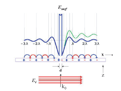
It is based on a solution to the 2-D Helmholtz equation in the near field and subject to the slab-like boundary conditions of a slit in an opaque screen. The basic expression describing the scalar wave is
| (1) |
with , and the amplitude of the wave propagating in the directions. Kowarz K95 has written down the solution to this equation for the case of an incident plane wave propagating in air () with amplitude and propagation vector impinging on a slit of width in an opaque screen. Specifying the coordinates as shown in Fig. 1, the field solution for the modes evanescent in at the boundary is
| (2a) | |||||
| (2b) | |||||
The evanescent modes are determined by a conservation-of-energy criterion,
| (3) |
The form of the inhomogeneous or evanescent field on the boundary is shown in Fig. 1. At transverse displacements from the slit , the evanescent component of the field at the surface can be represented to good approximation by the expression
| (4) |
that describes a damped wave with amplitude decreasing as the inverse of the distance from the launching edge of the slit, a phase shift with respect to the propagating plane wave at the midpoint of the slit and a wave vector . The wavelength of the CDEW on the surface where is the surface index of refraction (empirically, ). This surface wave is actually a composite superposition of modes evanescent in , with and directed along the axes.
| (5) |
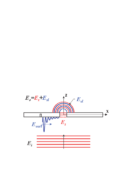
Equation 5 generalises the expressions of Eqs. 2a, 2b to include the evanescent components above the plane. When the composite evanescent wave encounters a surface discontinuity (a slit for example), a fraction of the surface wave is reconverted to a distribution of “homogeneous” or propagating modes at the site of the slit. In a practical experiment, any real planar structure has two surfaces: an “input side” in the half-space , containing the incoming plane wave, and an “output side” in the half-space , containing the far-field propagating modes issuing from the output surface and a photodetector. Experiments can be carried out by fabricating subwavelength grooves on the input side, the output side or both. The measurements reported here concern only the input-side experiments (Fig. 2). Results for output-side experiments will be reported later.
III Measurements and Results
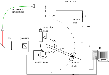
Measurements of the optical response of the slit-groove and hole-groove structures were carried out using a home-built goniometer shown in Fig. 3, details of which are described in the caption of Fig. 3 and in the Methods section.
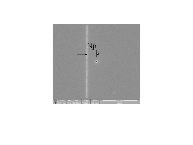
We have carried out a series of measurements on simple 1-D structures to test the “signature” predictions of the CDEW model, viz. (1) a composite surface wave expressed by Eq. 5 and approximately represented by a damped wave, Eq. 4; (2) a phase shift of between the CDEW and the driving source plane wave and (3) a wave amplitude that decreases inversely with distance from the launching groove. Figures 5, 5 show one of the series of structures consisting of one slit and one groove and one hole and one groove, respectively. The slit-groove distance or hole-groove distance is indicated as where is the basic unit of distance increment, the “pitch,” and is the number of increments. The pitch was taken to be 104 nm, approximately one-eighth the wavelength of the surface wave and was varied from 4 to 59. Structural details of these devices are described in the captions of Figs. 5, 5 and in the Methods section.
The slit(hole)-groove structures were mounted facing the input side and exposed to plane-wave radiation from the focused TEM00 laser source. Measurements of light intensity on the output side in the far field, 200 mm from the plane of the structures, were carried out on the slit-groove structures using the goniometer setup described in the Methods section. The results are shown in Figs. 7, 7.
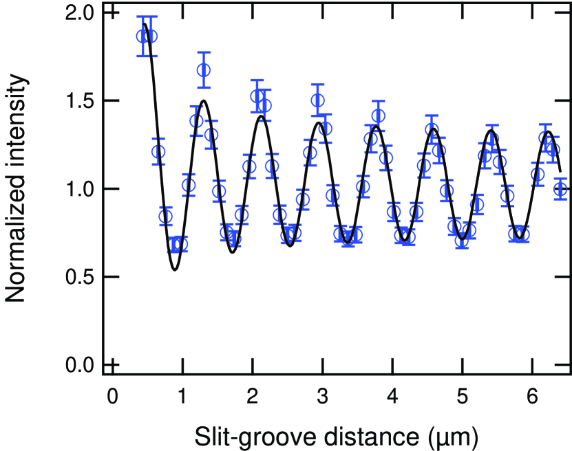

They show an oscillatory fringe pattern with amplitude damping out to a distance of m and maintaining an essentially constant amplitude from that point out to the distance limit of the measurements. As indicated in Fig. 2, the fringe pattern results from interference between the mode directly propagating through the slit (hole) at the input side and a surface wave originating from the single-groove structures . The wave is reconverted to a propagating mode at the slit or hole, and it is this propagating mode that interferes with . The frequency and phase of the interference pattern is a function of the slit (hole)-groove optical path and any intrinsic phase shift of the surface wave itself. The normalised intensity of the superposition term is given by
| (6) |
where is the fractional amplitude of the surface wave launched from the incoming field at the groove site, and is the further fraction of this surface wave reconverted to a propagating wave in the slit, . The fractional amplitude of the directly transmitted component is and the phase difference between and is the sum of two terms,
| (7) |
The first term is the phase accumulated by the surface wave propagating from the groove to the slit (hole) and the second term is any phase shift intrinsic to the surface wave. The term includes the “signature” shift of the CDEW plus any phase shift associated with the groove width and depth. Figures 7, 7 present a direct measure of the normalised amplitude damping with distance, and the period and phase of the oscillations, from which the wavelength of the surface wave, the phase , and the effective surface index of refraction can be determined. Analysis of the frequency spectrum of the fringe pattern for the slit(hole) structures results in the determination of a surface wavelength nm and an effective surface index of refraction . The amplitude of the oscillatory term depends on the slit(hole)-groove distance, and Figs. 7, 7 show that falls of with increasing distance. This fall-off is fit to an expression with two terms: an inverse distance dependence term plus a constant term.
| (8a) | |||||
| (8b) | |||||
The best-fit values for are indicated in the captions of Figs. 7, 7 and in Table 1 for slit and hole structures, respectively. The subscript and superscripts on refer to input-side, slit and hole measurements, respectively.
IV Discussions and Conclusions
The measured interference fringes on slit(hole) structures exhibit the presence of a surface wave with wavelength nm and therefore a surface index of refraction . The amplitude behavior of these fringes is also similar. Both the slit-groove and hole-groove structures exhibit an initial amplitude fall-off with increasing distance, damping to an essentially constant amplitude at a distance m. This behavior is fit to the expressions in Eqs. 8a, 8b. The fitting procedure is a linear regression varying the relative contributions of the constant and decaying amplitude terms, and and the intrinsic phase shift . The results are summarized in Table 1.
| parameter | slit structure | hole structure | SPP model |
|---|---|---|---|
| (nm) | |||
| (m) | |||
| Reference | Labs(m) | Lscat(m) | Lrad(m) | |||
|---|---|---|---|---|---|---|
| 111Measurements on silver films used in these experiments carried out at Caltech on a Sentech SE850 ellipsometer, 05 September 2005. | -33.27 | 1.31 | 1.0154 | 109 | ||
| JC75 | -34. | 0.46 | 1.015 | 326 | ||
| P85 | -32.4 | 1.74 | 1.0158 | 78.0 |
How do these results compare to CDEW or SPP models? In the CDEW picture, the groove launches a surface wave on the input side of the silver film that is detected by interference with the directly transmitted wave through the hole or slit, in the far field, on the output side of the structure. The amplitude of this surface wave is predicted to damp as the inverse distance between the groove and the slit or hole. Figures 7, 7 show an initial decrease in amplitude with increasing distance out to about m, but that the amplitude thereafter remains essentially constant. The solid curves in Figs. 7, 7 fit this amplitude decrease to an inverse distance dependence (Eqs. 8a, 8b). However, the damping might also plausibly fit an exponential decrease which would be expected from surface plasmon dissipative processes such as absorption by the silver film or scattering due to surface roughness. In order to check this possibility we have measured the properties of the silver films used in these studies. Table 2 summarises these properties and compares them to previously reported measurements JC75 ; P85 . The dielectric constant at 852 nm was measured by ellipsometery and surface roughness parameters determined by atomic force microscopy (AFM). The root-mean-square (rms) height of the films was measured to be nm and the correlation length nm. From the imaginary term of the dielectric constant and the parameters the expected propagation lengths of surface plasmons against absorption, surface scattering, and reradiation, , can be calculated Raether88 . It is clear from columns 5-7 of Table 2 that these loss processes cannot account for the observed damping within m of hole-groove distance.
The constant amplitude beyond m is consistent with a persistant surface wave. Indeed we have recorded measurements (not presented here) of the surface wave persisting at least to m slit-groove distance. It is important to emphasise, however, that and deviate significantly for those expected for a pure SPP on a plane silver surface. Interferometry measurements of the surface waves on “output side” slit-groove structures (not reported here) confirm the value of in Table 1, and we believe that conventional, infinite-plane SPP theory Raether88 is not adequate to explain these results. We note that persistent surface waves over m distances have also been reported in a double slit experiment SKD05 and interpreted as SPPs LHR05 .
As indicated in Table 1, intrinsic phase for the slit-groove and hole-groove structures respectively are and . Although one contribution to these phase shifts may be the CDEW “signature” phase shift of , it is known from earlier studies that the specific form (width and depth) of the grooves themselves, can introduce phase shifts into the scattered wave VLE03 . We have determined the nature of these groove-induced phase shifts and resonances by measuring interference fringes arising from surface waves launched on the “output-side” of slit-groove structures. These results, that will be reported in a subsequent publication, support the existence of an intrinsic phase shift close to .
The interpretation that emerges from these results is that the subwavelength groove originates persistant, long-range surface waves by a two-step process: (1) the incoming TM polarised plane wave scatters from the groove and generates in its immediate vicinity on the surface a broad, CDEW-like distribution of diffracted evanescent waves, and (2) this broad-band local surface “emitter” excites, within a distance of m, a long-range surface wave response. The near-term rapid amplitude decrease in the interference fringes of Figs. 7, 7 is evidence of this evanescent surface wave diffraction very near the groove. Persistant amplitude out to tens of microns is evidence for some kind of surface wave guided mode. It is significant to note that the wavelength and phase of the interference fringes do not shift over the entire range of the measurements. The initial diffracted surface wave components extend over a broad range of evanescent modes, , including the conventional . Therefore it is to be expected that the local surface wave emitter excites this surface mode. We emphasise, however, that our measurements show that the wavelength of this persistant wave does not correspond to and that, when the phase lag associated the groove itself is taken into account, the intrinsic phase of the surface wave with respect to the directly transmitted wave is close to . The disaccord between and is for the present a matter of speculation. Perhaps plasmon “leaky waves” Petit80 that transport energy very slowly away from the surface contribute to the spectrum of long-range surface excitation resulting in an effective wavelength shift; or perhaps, despite our ellipsometry measurements, the surface index of refraction of the metal film is slightly modified by some uncontrolled chemical or material process MM00 . At a more practical level, these results indicate that it might be much easier to couple to surface guided waves than was previously thought. Conventional wisdom asserts that because the SPP lies to the right of the “light line” on the metal surface dispersion curve, a grating or prism is needed to achieve efficient optical coupling Raether88 . A simple abrupt discontinuity in the surface, such as a slit or groove, appears to serve as an efficient coupler. Further studies are needed to understand the properties of the generated long-range persistant wave and to optimise the efficiency of this groove-coupling process.
V Methods
V.1 Structure fabrication
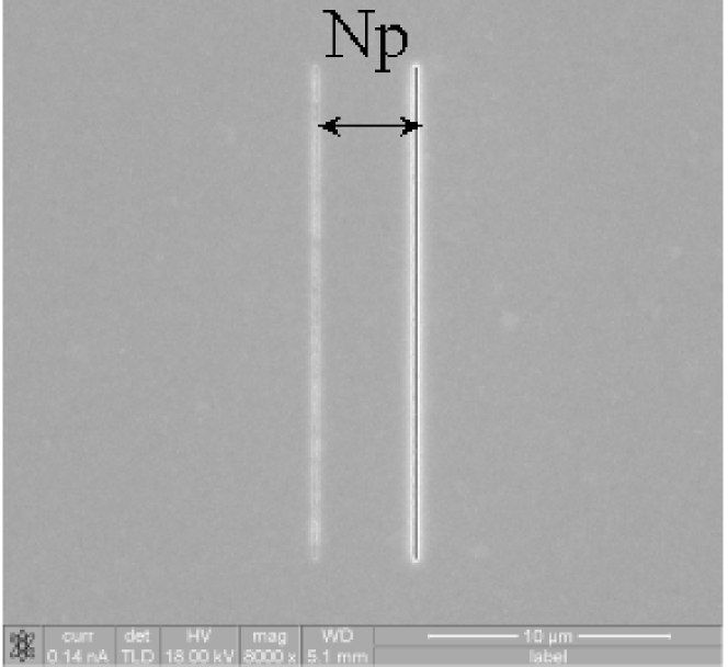
The structures consist of a single subwavelength slit or hole flanked by one subwavelength groove. The grooves have a width of 100 nm and a nominal depth of 100 nm for the slit-groove structures and 70 nm for the hole-groove structures. The slit-groove distance () or hole-groove distance () is systematically incremented in the fabrication process. The subwavelength structures are fabricated by focused ion beam (FIB) milling (FEI Nova-600 Dual-Beam system, Ga+ ions, 30keV) into a layer of silver evaporated onto flat fused silica microscope slides. A low beam current (50 pA) was used in order to achieve surface features defined with a lateral precision on the order of 10 nm and characterised by near-vertical sidewalls and a minimal amount of edge rounding. Since it enables delivery of a variable ion dose to each pixel of the writing field, FIB milling conveniently allows the multiple-depth topography characteristic of the present devices to be formed in a single, self-aligned step. A 2-D matrix of structures is milled into the silver layer. Each matrix consists of 63 structures, nine columns, separated by 1.5 mm, and seven rows, separated by 2 mm. The first column contains only the slit with no flanking grooves. Light transmission through the slits in this column is used to normalise the transmission in the remaining columns. Variations in transmission through each of the elements in the “slits only” column provide a measure of the uniformity of the FIB fabrication process. Each entire matrix of structures is flanked on one side by a small round hole and on the other by a line grating for absolute reference positioning and angular alignment of the structure matrix with respect to the input laser beam. The square microscope slides themselves, commercially available from SPI Supplies, are 25 mm on a side and 1 mm thick.
V.2 Measurement Setup
Details of the experimental setup are as follows. Output from a diode laser source, temperature stabilised and frequency-locked to 2P crossover feature in a Cs saturated absorption cell, is modulated at 850 Hz by a mechanical chopper, fed to a monomode optical fibre, focused and finally linearly polarised before impinging on the subwavelength structure mounted in the sample holder. The beam waist diameter and confocal parameter of the illuminating source are 300 m and 33 cm, respectively. Throughout this series of measurements the laser power density was maintained Wcm-2. The sample holder itself is fixed to a precision x-y translator, and multiple structures, FIB-milled in a 2-D array on a single substrate, are successively positioned at the laser beam waist. The optical response of the structures is synchronously detected by a photodiode and registered on a laboratory computer as indicated in Fig. 3.
Acknowledgements.
Support from the Ministère délégué à l’Enseignement supérieur et à la Recherche under the programme ACI-“Nanosciences-Nanotechnologies,” the Région Midi-Pyrénées [SFC/CR 02/22], and FASTNet [HPRN-CT-2002-00304] EU Research Training Network, is gratefully acknowledged as is support from the Caltech Kavli Nanoscience Institute and from the AFOSR under Plasmon MURI FA9550-04-1-0434. Discussions and technical assistance from P. Lalanne, R. Mathevet, F. Kalkum, G. Derose, A. Scherer, D. Pacifici, J. Dionne, R. Walters and H. Atwater are also gratefully acknowledged.References
- (1) Ebbesen, T. W., Lezec, H. J., Ghaemi, H. F., Thio, T., and Wolff, H. J. Extraordinary optical transmission through sub-wavelength hole arrays. Nature 391, 667-669 (1998).
- (2) Thio, T., Pellerin, K. M., Linke, R. A., Ebbesen, T. W., and Lezec, H. J. Enhanced light transmission through a single subwavelength aperture. Opt. Lett. 26, 1972-1974 (2001).
- (3) Ghaemi, H. F., Thio, T., Grupp, D. E., Ebbesen, T. W., and Lezec, H. J. Surface plasmons enhance optical transmission through subwavelength holes. Phys. Rev. B 58, 6779-6782 (1998).
- (4) Raether, H. Surface Plasmons on Smooth and Rough Surfaces and on Gratings, (Springer-Verlag, Berlin, 1988).
- (5) Barnes, W. L., Dereux, A., and Ebbesen, T. W. Surface plasmon subwavelength optics. Nature 424, 824-830 (2003).
- (6) Treacy, M. J. Dynamical diffraction in mateallic optical gratings. Appl. Phys. Lett. 75, 606-608 (1999).
- (7) Treacy, M. J. Dynamical diffraction explanation of the anomalous transmission of light through metallic gratings. Phys. Rev. B 66, 195105-1–195105-11 (2002).
- (8) Cao, Q., and Lalanne, P. Negative role of surface plasmons in the transmission of metallic gratings with very narrow slits. Phys. Rev. Lett. 88, 057403-1–057403-4 (2002).
- (9) García-Vidal, F. J., Lezec, H. J., Ebbesen, T. W.,and Martin-Moreno, L. Multiple paths to enhance optical transmission through a single subwavelength slit. Phys. Rev. Lett. 90, 213901-1–213901-4 (2003).
- (10) Chang,S-H., Gray, S. K., and Schatz, G. C., Surface plasmon generation and light transmission by isolated nanoholes and arrays of nanoholes in thin metal films. Optics Express, 13, 3150-3165 (2005).
- (11) Lezec, H. J. and Thio, T., Diffracted evansecent wave model for enhanced and suppressed optical transmission through subwavelength hole arrays. Optics Express 12, 3629-3651 (2004).
- (12) Mandel, L. and Wolf, E. Optical Coherence and Quantum Optics, pp. 109-120 (Cambridge University Press, Cambridge England, 1995).
- (13) Kowarz, M. W. Homogeneous and evanescent contribution in scalar near-field diffraction. Applied Optics 34, 3055-3063 (1995)
- (14) Johnson, P. and Christy, R. Optical constants of the noble metals. Phys. Rev. B 11, 1315-1323 (1975).
- (15) Palik, E. (ed.) Handbook of Optical Constants of Solids (Academic Press, Inc., New York, 1985.
- (16) Schouten, et al., Plasmon-Assisted Two-Slit Transmission: Young’s Experiment Revisited. Phys. Rev. Lett. 94, 053901–1-4 (2005).
- (17) Lalanne, P., Hugonin, J. P., Rodier, J. C., Theory of Surface Plasmon Generation at Nanoslit Apertures. Phys. Rev. Lett. 95, 263902-1–263902-4 (2005)
- (18) Hibbins, A.P., Sambles, J.R., and Lawrence, C. R., Gratingless enhanced microwave transmission through a subwavelength aperture in a thick metal plate. Appl. Phys. Lett. 81, 4661-4663 (2002).
- (19) Abajo, F. J. García de, Light transmission through a single cylindrical hole in a metallic film. Optics Express 10, 1475-1484 (2002).
- (20) Popov, E., Nevière, M., Boyer, P., and Bonod, N., Light transmission through a subwavelength hole. Optics Comm. 255, 338-348 (2005).
- (21) Petit, R. Electromagnetic Theory of Gratings, pp. 136-144 (Springer-Verlag, Berlin, 1980)
- (22) Mehan, N. and Mansingh, A., Study of tarnished films formed on silver by exposure to with the surface-plasmon resonance technique. Appl. Optics 39, 5214-5220 (2000).