Beam test results of the irradiated Silicon Drift Detector for ALICE
Abstract
The Silicon Drift Detectors will equip two of the six cylindrical layers of high precision position sensitive detectors in the ITS of the ALICE experiment at LHC. In this paper we report the beam test results of a SDD irradiated with 1 GeV electrons. The aim of this test was to verify the radiation tolerance of the device under an electron fluence equivalent to twice particle fluence expected during 10 years of ALICE operation.
, , , , , , , , , , , , , , , , , , .
For the ALICE Collaboration ††thanks: Corresponding author. E-mail: skushpil@ujf.cas.cz
1 Introduction
The Inner Tracking System (ITS) is the central detector of ALICE [1, 2]. Its basic functions are the secondary vertex reconstruction of hyperon and charm decays, the particle identification, the tracking of low-momentum particles and the improvement of the momentum resolution. The Silicon Drift Detectors (SDDs) will equip the third and the fourth layers of the ITS. They are very high-resolution non ambiguous two dimensional readout sensors adapted to high track density experiments with low rate because of their relatively slow readout. Moreover, the operational mode allows a radical reduction in the number of readout channels. The ALICE SDDs have to provide a spatial precision of about for both coordinates. Performance of different SDD prototypes has been studied with particle beams since 1997 [3, 4, 5]. In this paper we present the results obtained for detector irradiated by 1GeV electron beam.
2 Description of the detector
The ALICE SDD final prototypes[6] were produced by Canberra
Semiconductors on thick 5” thick NTD wafers with
a resistivity of 3 kcm.
Their active area is , i.e.83% of total area.
The active area is split into two adjacent 35 mm long drift regions,
each equipped with 256 collecting anodes ( pitch),
with built-in voltage dividers for the drift and the guard regions.
Design of the cathode strips prevents any punch-through which
would deteriorate the voltage divider linearity.
Due to the strong temperature variation of detector’s drift
velocity(), the monitoring of this quantity is
performed by means of three rows of 33 implanted point-like MOS charge
injectors for each drift region [7, 8].
During SDD operation the hole component of the leakage current is collected
by the drift cathodes and enters the integrated divider.
This affects the linearity of the potential distribution on the cathodes themselves
and, therefore, the position measurement obtained from the drift time.
Thus it is
critical to monitor such changes in order to be able to
reconstruct potential on the detector at any given time of the experiment .
This is the purpose of the MOS injectors.
The SDD front-end electronics is based on two 64 channel ASICs named
PASCAL[9] and AMBRA[10].
Four pairs of chips per hybrid are needed to read out
one half of the SDD. Full description of the electronics
is given in the paper [11].
Important steps toward the mass production of the detectors is
evaluation of their radiation hardness.
For this study the SDD was irradiated using
1 GeV electron beam at the LINAC of the Synchrotron in Trieste.
To reproduce the ALICE radiation environment, the electron fluence
must be 10 times the pion fluence and 20 times the neutron fluence according
to the Non-Ionizing Energy Loss (NIEL) hypothesis [12]. For this study
the electron fluence accumulated by the SDD
is equivalent to the total particle fluence expected during 20 years
of the ALICE operation and corresponds to an absorbed dose in silicon
of about 500.
The laboratory measurements [13] of the anode current and
the voltage distribution on the integrated divider as well as
and the operation of the MOS injectors demonstrate
that the SDD is sufficiently radiation resistant for the full operation lifetime
of the ALICE experiment. Still, it was necessary to verify these expectations
with a beam test. Within 2002 and 2003 years, the same detector was tested twice
(before and after its irradiation with electrons) using
CERN SPS beam with .
The detector under test was placed on the beam line. A telescope,
made up of five pairs of single sided silicon strip detectors with
a strip pitch of , was used to reconstruct the tracks of passing
particles. Precision in the determination of the particle impact point in the
SDD plane was .
Since the size of the beam spot and the area
covered by the microstrip detectors were smaller than the SDD sensitive area,
the SDD was mounted on a mobile support. Its position was remotely
controlled and measured with a precision of about .
It should be noted that during June 2002 beam test only the central
anode region of the SDD was studied, and in this case 32-channel PASCAL prototype
was used. To study the irradiated SDD in August 2003 we used 64-channel PASCAL
to readout full anode array.
3 Beam test results
3.1 Cluster Size
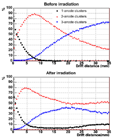
The electron cloud generated by an ionizing particle in the SDD undergoes a diffusion while drifting to the collection anodes. After the digitization of the anode signals, the cloud is represented by a two-dimensional set of amplitude values, called a ”cluster”. We compared cluster size in the non-irradiated and irradiated detector. Fig. 1 shows the relative amounts of clusters collected by one, two and three anodes as a function of the drift time. At a short drift distance the number of multi-anode clusters increases after irradiation due to increased diffusion coefficient. For a large drift distance a presence of one-anode clusters can be observed for irradiated detector because of a threshold cut and decrease of the signal amplitude.
3.2 Charge
Fig.2 shows changes in the charge collection in the SDD before and after irradiation. The collected charge decreases as a function of the drift distance.
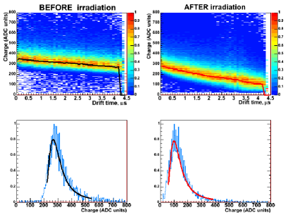
A charge collection inefficiency before irradiation was already observed in this detector on the test bench in the laboratory. The most probable reason is the presence of electron trapping centers in the silicon bulk, occasionally introduced in that particular wafer during detector fabrication. After irradiation a rapidity of charge loss increases by three times due to the increased electron trapping. The comparison of the most probable values of the registered charge shows that after irradiation the charge collection drops by 60% at the maximum drift distance.
3.3 Dopant inhomogeneity
Even though the ALICE SDDs are produced on NTD wafers, which should have a particularly uniform dopant concentration, the observed inhomogeneity characteristic effects deteriorate significantly the spatial resolution of the detectors [14, 5]. Inhomogeneity of the dopant concentration alters the uniformity of the main drift field and, thus, creates systematic deviations in the measurement of coordinates of the registered particle.
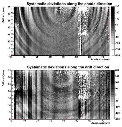
The differences between coordinates of a particle impact point measured by
the SDD and by the microstrip telescope (residuals) are presented in
Fig.3 for the irradiated SDD. They are plotted as functions of
the anode coordinate and the drift distance. The grey scale represents
magnitude of residuals for the anode coordinate (top plot) and
the drift coordinate (bottom plot).
The empty areas correspond to non-working channels or missing experimental data.
Deviation of a few tens of in average and with maximum values up
to are observed and must be corrected to reach
the required spatial resolution of .
Recently custom ingots have shown much lower doping fluctuation.
The circular structures centered in the middle of the wafer clearly visible
in this plot can be attributed to the characteristic radial dependence of the
dopant concentration fluctuations [5, 14, 15].
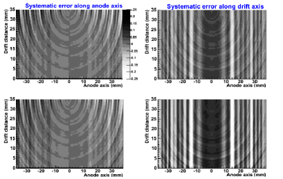
In addition to radial structures, the maps present also a deviation pattern in a form of vertical lines. Since the effect is similar for all electrons collected by a certain anode and looks correlated with the intersection of the circular structure by the anode line, we can conclude that the local field and its fluctuations in the collection region is at the origin of this effect. We can also clearly observe that, after irradiation, the magnitude of this linear pattern has increased. In order to understand whether this evolution of the position correction map is easily predictable, a charge transport simulation was performed (Fig.4), taking into account a realistic three-dimensional electrostatic field model in the detector. This field was generated by superimposing a potential fluctuation map to the solution of the Poisson equation assuming a homogeneous silicon bulk. To reproduce qualitatively the experimental fluctuation map, the superposition of four radial waves with different wavelengths was used. After irradiation, the difference of potential between adjacent cathodes is not anymore constant but assumes a linear evolution, responsible for a linear dependence of the electrostatic drift field as a function of the drift distance. The drift field is weaker close to the anodes and stronger for the maximum drift distance. In order to optionally reproduce this effect, a parabolic component can be added to the potential in the simulation. The transport calculation of the electrons in the silicon bulk takes into account the electrostatic field deriving from the previously described potential. The trajectory of the electrons was calculated from every node of a grid covering the half SDD surface, to the collection anodes. Assuming a linear trajectory and a constant drift velocity, the initial position of the electron can be estimated from its arrival time and anode axis coordinate. The two coordinates of the difference of the predicted and the actual positions as a function of the initial position are plotted in Fig.4. Two cases are shown: before and after irradiation. The vertical deviation pattern can effectively be observed and its magnitude increased when the parabolic potential is added. As a conclusion, we can say that the irradiation has only an indirect effect on the deviation map through its influence on the voltage divider but no significant effect on the bulk material properties.
3.4 Spatial resolution
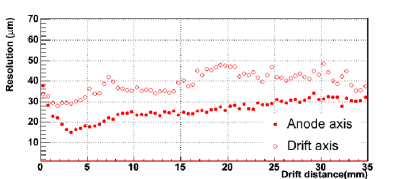
The detector spatial resolution is defined as the of the difference between the position measured by the SDD and the impact point coordinate reconstructed with the microstrip telescope. Fig.5 shows the resolution along the anode and the drift time directions obtained after correction of the systematic deviation for one half of the irradiated SDD. The resolution along the anode direction has values better than over more than 70% of the whole drift path and the best value reachs at from the anodes. The deterioration of the resolution at a small drift distance is due to the a small size of the electron cloud collected on the anodes. The resolution along the drift direction has a value increasing from to .
+
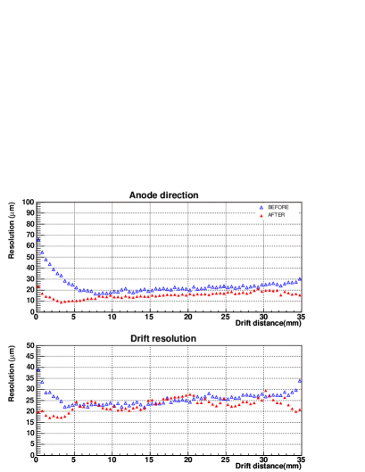
For narrow central region of the SDD anodes it is possible to compare the spatial resolution before and after irradiation (Fig. 6). One can observe that after irradiation in the vicinity of the anodes, the value of the resolution along both direction becomes better. This behaviour is due to decreasing fraction of the narrow clusters after irradiation. For longer drift distances, the values of the resolution are very similar to those for non-irradiated detector. Taking into account that the SDD was irradiated with dose equivalent to 20 years of the ALICE operation, the resolution remains within specifications of technical design for the ALICE ITS. Even with the very strong effect of the dopant inhomogeneity which increases with irradiation, it is demonstrated that the systematic deviations in coordinate measurements can be corrected and a satisfactory resolution can be achieved along both anodic and drift directions.
4 Conclusion
Extensive study of the performance of a silicon drift detector irradiated with dose equivalent to 20 years of the ALICE operation was carried out using a 64-channel PASCAL front-end chip. The results show than in spite of increased charge loss the values of the spatial resolution fully satisfy the ALICE technical design requirements, once the correction of the systematic errors is performed. The detector was found to be sufficiently radiation hard for the ALICE experiment.
Acknowledgements.
This work was supported by the grant of the Ministry of education of the Czech Republic 1P04LA211 and by the Institutional Research Plan AV0Z10480505.
References
- [1] ALICE Collaboration, CERN/LHCC, 99/12
- [2] F. Tosello et al., Nucl. Instr. and Meth. A473 (2001) 210-218.
- [3] A. Vacchi et al., Nucl. Instr. and Meth. A326 (1993) 267-272
- [4] V. Bonvicini et al., Nucl. Instr. and Meth. A459 (2001) 494-501
- [5] E. Crescio et al., Nucl. Instr. and Meth. A 539 1/2 (2005) 250-261
- [6] A. Rashevsky et al., Nucl. Instr. and Meth. A 461 (2001) 133-138
- [7] E. Gatti et al., Nucl. Instr. and Meth. A 295 (1990) 489-491
- [8] V. Bonvicini et al., Nucl. Instr. and Meth. A439 (2000) 476.
- [9] A. Rivetti et al., CERN-LHCC-2000-041
- [10] G. Mazza et al., CERN-LHCC-2001-034
- [11] A. Rivetti et al., Nucl. Instr. and Meth. A 541 (2005) 267-273
- [12] G.P. Summers et al., IEEE Nucl.Sci. NS-40 (6) (1993) 1372
- [13] C. Piemonte et al., Nucl. Instr. and Meth. A485 (2002) 133-139
- [14] D. Nouais et al., Nucl. Instr. and Meth. A 461 (2001) 133-138
- [15] S. Kouchpil et al., Part. Nucl. Lett. 2004, V.1, No 4 (121), P. 70-79